Journal of the Korean Crystal Growth and Crystal Technology Vol. 22, No. 1 (2012) 1-4
http://dx.doi.org/10.6111/JKCGCT.2012.22.1.001
Growth of O- and Zn-polar ZnO films by DC magnetron sputtering
Jinyeop Yoo, Sungkuk Choi, Soohoon Jung, Youngji Cho, Sangtae Lee*, Gyungsuk Kil**, Hyunjae Lee***, Takafumi Yao**** and Jiho Chang†
Department of Nano-semiconductor Engineering, National Korea Maritime University, Busan 606-791, Korea
*Department of Offshore Plant Management, National Korea Maritime University, Busan 606-791, Korea
**Division of Electrical and Electronics Engineering, National Korea Maritime University, Busan 606-791, Korea
***PAN-Xal Co., Ltd., Suwon 443-380, Korea
****Center for Interdisciplinary Research, Tohoku University, Sendai 980-8577, Japan (Received October 12, 2011)
(Revised November 4, 2011) (Accepted November 18, 2011)
Abstract O- and Zn-polar ZnO films were grown by DC magnetron sputtering. Growth of high-quality, single-crystal ZnO thin films were confirmed by XRD and pole figure analysis. O-polar ZnO was grown on an Al2O3 substrate, which was confirmed by a slow growth rate (378 nm/hr), a fast etching rate (59 nm/min), and by the hillocks on the surface after etching. Zn-polar ZnO was grown on a GaN/Al2O3 substrate, which was confirmed by a fast growth rate (550 nm/hr), a slow etching rate (28 nm/min), and by pits on the surface after etching. Results from the present study show that it is possible to use DC-sputtering to grow ZnO film with the same polarity as other epitaxial growth methods.
Key words ZnO, DC magnetron sputtering, Polarity
1. Introduction
ZnO has always been regarded as a potential candi- date for GaN growth [1] since it has a lattice parameter and a crystal structure that is similar to that of GaN.
Therefore, the growth of GaN on a ZnO template has attracted special interest, because it could provide an easy way to separate GaN from the substrates. Various studies have examined the growth of GaN on a ZnO/
Al2O3 template using hydride vapor phase epitaxy (HVPE) [2, 3] and molecular beam epitaxy (MBE) [4]. To make this technique commercially viable, a high-quality ZnO layer that can be produced using a less-expensive method is needed. It is worth noting that the growth of high-qual- ity ZnO on a Al2O3 substrate is not a simple process.
Therefore, the sputtering of single crystalline ZnO thin film [5] has attracted special interest. Many groups have reported the successful growth of single-crystalline ZnO by high-temperature sputtering; even a light emitting diode (LED) has been produced based on sputtered ZnO thin films [5, 6]. However, a high-quality sputtered ZnO layer will not satisfy all requirements. In a previous experi- ment [7], this group found that under highly volatile cir- cumstances, such as those encountered during hydride
vapor phase epitaxy (HVPE), a Zn-polar ZnO surface is essential for its stability during the growth of high-qual- ity GaN on ZnO. However, the production of Zn-polar ZnO thin film by sputtering has not been investigated.
In the present study, the growth of single-crystalline Zn- polar and O-polar ZnO films by DC magnetron sputter- ing was investigated, along with the crystal quality and polarity of sputtered ZnO films grown at a high-growth temperature in a high-vacuum sputtering chamber.
2. Experimental
ZnO thin films were sputtered on Al2O3 (0001) sub- strates and Ga-polar GaN templates by DC magnetron sputtering. The substrates were degreased, but no other pre-treatment, including chemical etching, was performed.
The background pressure of the sputter was as low as
< 1 × 10⁻¹⁰torr. The growth temperature was 900oC, the plasma power was 50 W, and the gas flow rate was 11 sccm (Ar : O2= 10 : 1). The sputtering condition of the ZnO film was optimized in terms of the surface mor- phology and growth rate of the ZnO film. High-resolu- tion X-ray diffraction (HRXRD) measurement was used to evaluate the crystallinity of the ZnO film. In the present study, (002) and (101) omega scans and a (101) pole figure scan all were measured. The polarity of the ZnO films was estimated and determined by evaluating
†Corresponding author
†Tel: +82-51-410-4783
†Fax: +82-51-410-4833
†E-mail: [email protected]
2 Jinyeop Yoo, Sungkuk Choi, Soohoon Jung, Youngji Cho, Sangtae Lee, Gyungsuk Kil, Hyunjae Lee, Takafumi Yao and Jiho Chang
the growth rate, etching rate, and surface morphology of each film. Chemical etching was performed using a diluted HCl solution (0.3 Vol. %), and the thickness and surface morphologies of the samples were measured by profiler and atomic force microscopy, respectively.
3. Results and Discussion
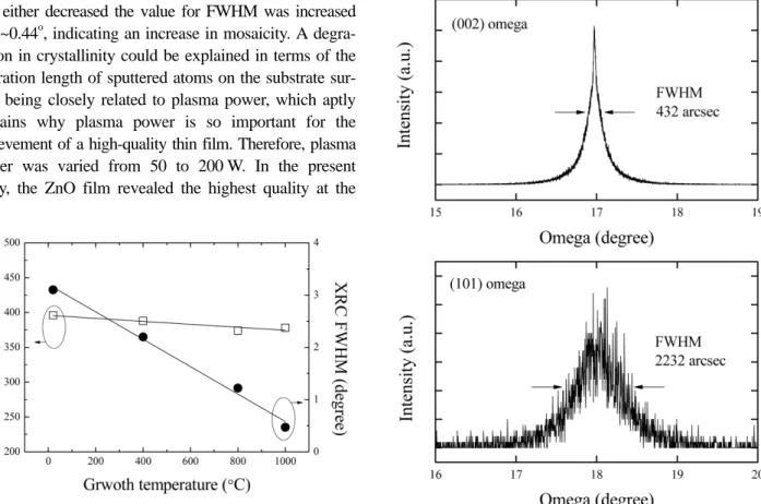
Figure 1 shows the change in growth rate and crystal quality as a function of the growth temperature. In the present study, to determine the conditions for growth, plasma power and growth temperature were optimized.
The influence of plasma power has been investigated by Cebulla et al. [8], who showed that a higher ion-to-neu- tral ratio ji/jn of the growing film strongly influences the structural and electrical properties of ZnO films. Also, Kim et al. reported that the full width at half maximum (FWHM) of the XRD rocking curve for a ZnO thin film was optimized when the film was deposited at 550oC with plasma powers of 80 W. They reported that the best-quality sample showed the narrowest rocking curve for FWHM, 0.16o (576 arcsec), indicating a highly c- axis-oriented columnar structure. Also, as plasma power was either decreased the value for FWHM was increased 0.30~0.44o, indicating an increase in mosaicity. A degra- dation in crystallinity could be explained in terms of the migration length of sputtered atoms on the substrate sur- face being closely related to plasma power, which aptly explains why plasma power is so important for the achievement of a high-quality thin film. Therefore, plasma power was varied from 50 to 200 W. In the present study, the ZnO film revealed the highest quality at the
lowest plasma power within the experimental range 50 W.
Further investigation into the sputtering of ZnO was performed. Fig. 1 shows the varied growth rates and the changes in x-ray rocking curve for FWHM as a func- tion of growth temperature. As Fig. 1 shows, when the temperature was changed from room temperature to 1,000oC, the growth rate decreased slightly from 395 to 360 nm/hr, while the FWHM value was narrowed remark- ably. It shows that an energetic than kinetic growth pro- cess determines the crystal quality of a sputtered thin film.
Figure 2 shows the XRC of ZnO (002) and (101) grown on c-Al2O3 substrates. The plasma power was 50W, growth temperature was 900oC, and the Ar/O2 ratio was 10. The sample thickness was 586 nm. The FWHMs of (002) and (101) rocking curves were 432 and 2232 arcsecs, respectively. These results are compa- rable to the previous results [9], which show that sput- tered ZnO has a strong c-axis-aligned columnar structure.
Figure 3 shows the (101) diffraction plane pole figure of the sample described in Fig. 2. It shows that the sam- ple clearly has a 6-fold symmetry, which means that the films have a single crystalline phase [9, 15]. Note that, in
Fig. 1. Growth rate and FWHM of XRC variation of the sput- tered films in a function of growth temperature. For all sam- ples, growth temperature was 900oC, and Ar : O2 ratio was
10 : 1.
Fig. 2. (0002) and (10-11) X-ray rocking curve results of sput- tered ZnO on c-Al2O3. The FWHM of (0002) reflection was as
narrow as 432 arcsec.
Growth of O- and Zn-polar ZnO films by DC magnetron sputtering 3
the present experiment, only when the growth tempera- ture was higher than 800oC was a clear 6-fold symme- try observed. However, when the growth temperature was lower than 800oC, a 6-fold symmetry was not observed except other growth parameters. This fact implies that the crystal quality of sputtered films is determined energetically.
The growth of Zn- and O-polar ZnO films was attempted using the described growth conditions. First, Al2O3 and GaN/Al2O3 substrates were used for the growth of O-polar and Zn-polar ZnO, respectively. Generally, ZnO grown on an Al2O3 substrate shows O-polar, while ZnO grown on a GaN template follows the polarity of GaN. A 2µm- thick MOCVD GaN template was expected to support the growth of Zn-polar ZnO because it has Ga polarity.
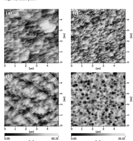
Figure 4 shows AFM images of ZnO films grown on Al2O3 and GaN/Al2O3 substrates. Figure 4(a) and (c) show the surface morphologies of as-grown ZnO films on Al2O3 (Fig. 4(a)) and on a GaN template (Fig. 4(c)).
Those two samples were simultaneously grown on the
Fig. 4. AFM images of as-deposited and etched ZnO films. (a) as deposited ZnO/Al2O3, (b) etched ZnO/Al2O3, (c) as-deposited ZnO/GaN/Al2O3, and (d) etched ZnO/GaN/Al2O3.
Fig. 3. X-ray pole figure pattern recorded from the (10-11) reflection. 6-fold symmetry indicates that the ZnO film has
single crystalline phase.
4 Jinyeop Yoo, Sungkuk Choi, Soohoon Jung, Youngji Cho, Sangtae Lee, Gyungsuk Kil, Hyunjae Lee, Takafumi Yao and Jiho Chang
same sample holder. Although the AFM results indicate a difference in grain size, presumably due to the differ- ence in the lattice mismatch between the film and the substrate, a considerable morphological change was not observed. However, the growth rate for ZnO/Al2O3 was 378 nm/hr, while that for ZnO/GaN was as fast as 550 nm/
hr. Furthermore, attempts were made to etch those sam- ples to evaluate the etching rate. The etching rate for each sample was 28 nm/min for a ZnO/GaN sample and 59 nm/min for a ZnO/Al2O3 sample. Also, the etched surfaces differed significantly. The etched surfaces for the ZnO/Al2O3 and ZnO/GaN samples revealed hillocks (Fig. 4(b)) and pits (Fig. 4(d)), respectively. Previous stud- ies, O-polar ZnO films have shown mainly a slow growth rate and a fast etching rate [10-14], while Zn-polar ZnO films were just the opposite and included pits [13, 14].
Consequently, the polarity of ZnO grown on either Al2O3 or GaN was either O-polar or Zn-polar, respectively.
4. Summary and Conclusion
Sputtering conditions for single-crystal-phase ZnO film was investigated. Under optimum growth conditions, the (002) and (101) FWHM of sputtered ZnO films were 432 and 2232 arcsec, respectively. Also, the (101) pole figure scan clearly showed 6-fold symmetry, which indicates that ZnO has a single-crystal phase. Also, O- and Zn-polar ZnO films were grown by DC magnetron sputtering using Al2O3 and GaN/Al2O3 substrates, respectively. The growth rate, the etching rate, and the surface morphology of the ZnO films indicated that the ZnO/Al2O3 and ZnO/GaN/
Al2O3 films were O-polar and Zn-polar, respectively.
Acknowledgments
This research was supported by the Basic Science Research Program through the National Research Founda- tion of Korea (NRF) funded by the Ministry of Education, Science and Technology (No. 2010-0009828) and the MKE (The Ministry of Knowledge Economy), Korea, under the ITRC (Information Technology Research Center) sup- port program supervised by the NIPA (National IT Indus- try Promotion Agency) (NIPA-2012-C1090-1221-0015).
References
[ 1 ] T. Dethprohm, K. Hiramatsu, H. Amano and I. Akasaki,
“Hydride vapor phase epitaxial growth of a high qual- ity GaN film using a ZnO buffer layer”, Appl. Phys.
Lett. 61 (1992) 2688.
[ 2 ] T. Detchprohm, H. Amano, K. Hiramatsu and I.
Akasaki, “The growth of thick GaN film on sapphire substrate by using ZnO buffer layer”, J. Cryst. Growth 128 (1993) 384.
[ 3 ] S. Gu, R. Zhang, Y. Shi, Y. Zheng, L. Zhang and T.F.
Kuech, “Hydride vapor phase epitaxy growth of GaN on sapphire with ZnO buffer layers” Appl. Phys. A 74 (2002) 537.
[ 4 ] S.W. Lee, T. Minegishi, W.H. Lee, H. Goto, H.J. Lee, S.H. Lee, H.-J. Lee, J.S. Ha, T. Goto, T. Hanada, M.W.
Cho and T. Yao, “Strain-free GaN thick films grown on single crystalline ZnO buffer layer with in situ lift-off technique”, Appl. Phys. Lett. 90 (2007) 061907.
[ 5 ] K. Kim, J. Song, H. Jung, W. Choi, S. Park and J.
Song, “The grain size effects on the photoluminescence of ZnO/α-Al2O3 grown by radio-frequency magnetron sputtering”, J. Appl. Phys. 87 (2000) 3573.
[ 6 ] J.-H. Lim, C.-K. Kang, K.-K. Kim, I.-K. Park, D.-K.
Hwang and S.-J. Park, “UV electroluminesecence emis- sion from ZnO light-emitting diodes grown by high- temperature radiofrequency sputtering”, Adv. Mater. 18 (2006) 2720.
[ 7 ] X. Gu, M.A. Reshchikov, A. Teke, D. Johnstone, H.
Morkoc, B. Nemeth and J. Nause, “GaN epitaxy on thermally treated c-plane bulk ZnO substrates with O and Zn faces”, Appl. Phys. Lett. 84 (2004) 2268.
[ 8 ] R. Cebulla, R. Wendt and K. Ellmer, “Al-doped zinc oxide films deposited by simultaneous rf and dc excita- tion of a magnetron plasma: Relationships between plasma parameters and structural and electrical film properties”, J. Appl. Phys. 83 (1998) 1087.
[ 9 ] K.K. Kim, J.H. Song, H.J. Jung, W.K. Choi, S.J. Park and J.H. Song, “The grain size effects on the photolumi- nescence of ZnO/α-Al2O3 grown by radio-frequency magnetron sputtering”, J. App. Phys. 87 (2000) 3573.
[10] X. Wang, Y. Tomita, O.H. Roh, M. Ohsugi, S.B. Che, T.
Ishtani and A. Yoshikawa, “Polarity control of ZnO films grown on nitrided c-sapphire by molecular-beam epitaxy”, Appl. Phys. Lett. 86 (2005) 011921.
[11] H. Tampo, P. Fons, A. Yamada, K.K. Kim, H. Shibata, K. Matsubara, S. Niki, H. Yoshikawa and H. Kanie,
“Determination of crystallographic polarity of ZnO lay- ers”, Appl. Phys. Lett. 87 (2005) 141904.
[12] J.S. Park, J.H. Chang, T. Minegishi, H.J. Lee, S.H. Park, I.H. Im, T. Hanada, S.K. Hong, M.W. Cho and T. Yao,
“Growth of polarity-controlled ZnO films on (0001) Al2O3”, Journal of Electronic Materials 37 (2008) 736.
[13] H. Kato, M. Sano, K. Miyamoto and T. Yao, “Polarity control of ZnO on c-plane sapphire by plasma-assisted MBE”, J. Cryst. Growth 275 (2005) e2459.
[14] K. Sakurai, M. Kanehiro, K. Nakahara, T. Tanabe S.
Fujita and S. Fujita, “Effects of oxygen plasma condi- tion on MBE growth of ZnO”, J. Cryst. Growth 209 (2000) 522.
[15] J.H. Park, S.J. Jang, S.S. Kim and B.T. Lee, “Growth and characterization of single crystal ZnO thin films using inductively coupled plasma metal organic chemical vapor deposition”, Appl. Phys. Lett. 89 (2006) 121108.