1. INTRODUCTION
Recently, transparent-oxide-semiconductor-based transistors have shown much attention in application such as active-matrix organic light-emitting displays (AMOLED), active-matrix liquid-crystal displays (AMLCDs), and flexible displays [1-3]. Thin film transistors (TFTs) using oxide-semiconductor channels have been intensively investigated because oxide semiconductors such as amorphous In-Ga-Zn-O (a-IGZO) can be formed at a low-temperature process and show larger motilities than those of hydrogenated amorphous silicon TFTs [4].
One of the essential issues to be considered for realizing the improved performance is the influence of source/drain (S/D) electrodes, including materials, contact quality, and parasitic resistance. In general, heavily doped regions
below S/D electrodes were adopted to obtain good contact properties. Attempts to dope the selected contact regions of a-IGZO films by Ar plasma treatment have proven significant improvement in device performance [5].
However, this doping process possibly damages the film surface by sputtering ion (Ar
+) bombardment. Barquinha et al.[6] reported that various S/D electrodes affected the drain current of TFTs and that an annealing process improved the electrical properties. Park etal.[7] investi- gated the effects of S/D series resistance and transfer length on a-IGZO TFTs. So far, indium tin oxide (ITO), Au, Al, indium zinc oxide (IZO), and Pt/Ti were used as S/D electrodes for a-IGZO TFTs [5, 8, 9]. Although oxide based electrodes, such as ITO and IZO electrodes allow fully transparent TFTs, their large electron affinity of the oxide electrodes (and Au) causes non-ohmic behaviors in the linear regime of output characteristics due to the formation of the Schottky-like barrier between the electrodes and the a-IGZO films [9]. X. Zou etal. also reported that AZO/Al heterojunction S/D contacts showed the forming of a good ohmic contact and the improved mobility and the subthreshold gate voltage swing.
Furthermore, the ohmic contact properties could be improved by replacing electrode materials and/or by modifying the contact area. Among many efforts to develop new TCO materials, the multilayer of dielectric material/metal/dielectric material (DMD) has been suggested as one of candidates to overcome the limit in electrical resistivity of single layer TCOs ever reported
1Interface Research Center, Korea Insitute of Science and Technology, Sungbuk Gu, Hwarnagno 14 gil 5, Seoul 136-791, Korea
2Advanced Semiconductor Research Center, Division of Electrical and Computer Engineering, Hanyang University, 17 Haengang-Dong, Seongdong-Gu, Seoul 133-791, Korea
3Department of Physics, Yonsei University, Seoul 120-749, Korea
4Electronic Materials Research Center, Korea Insitute of Science and Technology, Sungbuk Gu, Hwarnagno 14 gil 5, Seoul 136-791, Korea +Corresponding author: [email protected]
(Received : Feb. 18, 2013, Revised : Mar. 13, 2013, Accepted : Mar. 14, 2013) This is an Open Access article distributed under the terms of the Creative Commons Attribution Non-Commercial License(http://creativecommons.org/licenses/by- nc/3.0)which permits unrestricted non-commercial use, distribution, and reproduction in any medium, provided the original work is properly cited.
http://dx.doi.org/10.5369/JSST.2013.22.2.105 pISSN 1225-5475/eISSN 2093-7563
Improved Electrical Properties of Indium Gallium Zinc Oxide Thin- Film Transistors by AZO/Ag/AZO Multilayer Electrode
Young-Soo No
1,2Jeong-Do Yang
3, Dong-Hee Park
1, Tae-Whan Kim
2, Ji-Won Choi
4, and Won-Kook Choi
1, +Abstract
We fabricated an a-IGZO thin film transistor (TFT) with AZO/Ag/AZO transparent multilayer source/drain contacts by rf magnetron sputtering. a-IGZO TFT with AZO/Ag/AZO multilayer S/D electrodes (W/L = 400/50 µm) showed a subs-threshold swing of 3.78 V/dec, a minimum off-current of 10-12A, a threshold voltage of 0.41 V, a field effect mobility of 10.86 cm2/Vs, and an on/off ratio of 9×
109. From the ultraviolet photoemission spectroscopy, it was revealed that the enhanced electrical performance resulted from the lowering of the Schottky barrier between a-IGZO and Ag due to the insertion of an AZO layer and thus the AZO/Ag/AZO multilayer would be very appropriate for a promising S/D contact material for the fabrication of high performance TFTs.
Keywords : a-IGZO TFT, AZO/Ag/AZO transparent electrode, Field effect mobility, Schottky barrier
because it allows both the overall carrier concentration and the mobility to be increased, prevailing to some extent the limitation imposed by ionized impurity scattering in metal- oxide single layers and can increase transparency in the visible range of the wavelength due to the anti-reflection principle of successive layer coating for high(n
1)/low(n
2)/high refractive index(n
1) [10]. Among the most widely studied dielectric films in DMD structures such as Al doped ZnO, Ga doped ZnO and ITO, Al-doped ZnO (AZO) thin film has become a good alternative for transparent electrode applications, due to its low resistivity on the order of 10
-4Ω·cm, inexpensive source materials, and high transpar-ency in the near UV and visible range.
This study investigates novel multilayer AZO/Ag/AZO S/D contacts to enhance the performance of a-IGZO TFTs.
The mobility, on/off current ratio and sub-threshold gate voltage swing of the a-IGZO TFTs with AZO/Ag/AZO layer S/D electrodes are investigated. The improved mobility and the sub-threshold gate voltage swing of the a- IGZO TFT with AZO/Ag/AZO S/D contacts compared to the TFTs with single-Ag S/D electrodes are elucidated by carefully examining the variation of potential barriers at the interface through ultraviolet photoemission spectroscopy (UPS).
2. EXPERIMENTAL
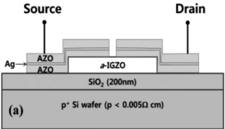
Fig. 1 shows a schematic cross-sectional view of the TFT structure. This was fabricated on the p-type boron doped silicon wafer with low resistivity (ρ~ 0.001 Ω·cm,) as the gate electrode. SiO
2(200 nm) thin film as an insulating layer was thermally grown on the Si substrate by a chemical vapor deposition. These substrates were then cleaned by acetone, methanol, ethanol and de-ionized water in an ultrasonic bath. Thin films of a-IGZO (40 nm- thick) were deposited as the active layer using rf magnetron sputtering with sintered InGaZnO
4(In
2O
3:Ga
2O
3:ZnO
=1:1:1 99.999%, purity) as the target material.
The initial vacuum level is lower than 1×10
-4Pa. Pre- sputtering was performed to remove any contamination on the target surface for 10 min prior to the deposition of the active layer. IGZO thin films were sputtered at room temperature in an argon atmosphere with an oxygen partial pressure of 5% corresponding to the working pressure of 0.67 Pa. The active layer was patterned by conventional photolithography and a lift-off process. The post-annealing process was carried out in pure O
2ambient using RTA
equipment at 300。C. The S/D electrodes were defined using a lift off process. To form the top S/D contact of Ag and AZO/Ag/AZO multilayers were deposited by rf magnetron sputtering. The Ag layer with a nominal 100nm was deposited on the patterned a-IGZO film by RF sputtering with an Ar ratio of 20 sccm. For the AZO/Ag/
AZO multilayer, the bottom AZO layer was sputtered at 80 W rf power and 0.53 Pa Ar plasma gas pressure. The Ag intermediate layer was successively deposited by rf magnetron sputtering at 20 W and 0.53 Pa Ar plasma gas pressure. Then, the top AZO layer was sputtered by the same method with the AZO first layer. The resistivity and optical transmittance of the AZO/Ag/AZO multilayer electrodes were measured by Hall measurements and UV/visible spectroscopy (Model: Perkin Elmer Lambda 18), respectively. Transmission electron microscopy (TEM: FEI Tecnai F20) was employed to investigate the structure of the multilayer electrodes. The electrical characteristics of a-IGZO films and TFT devices were measured using a Keithley 4200 precision semiconductor parameter analyzer in the dark. Work functions of Ag, AZO/Ag/AZO including IGZO thin films were determined from the positions the Fermi level measured from the tangent line extrapolation of the onset for the secondary electron peak in the ultraviolet photoemission spectroscopy (UPS, Kratos AXIS-NOVA) spectra. The photon energy of the UPS light source (He (I) radiation ) was hν=21.2 eV and the energy of the band pass filter in the analyzer was fixed at 20 eV.
3. RESULTS AND DISCUSSIONS
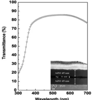
Fig. 2 presents the optical transmission spectra of the AZO/Ag/AZO thin film deposited on glass substrate. The
Fig. 1. Schematic diagram of the a-IGZO TFT with AZO/Ag/
AZO source-drain electrode.
inset in Fig. 2 shows a cross sectional TEM image of the AZO/Ag/AZO multilayer indicating that the thicknesses of each layer are approximately 47 nm and 11 nm for the AZO and Ag layer, respectively. Based upon the optical simulation using the Macleod program and experimental data, we carefully determined the optimal thickness of Ag and AZO thin films and tried to deposit at this condition.
The AZO/Ag/AZO thin film shows the electrical resistivity ρ=8.6×10
-5Ω·cm, carrier concentration n
e=8.0×
10
22/cm
3, and mobility
µ=20 cm
2/Vs.
Average transmittance of AZO/Ag/AZO thin film is ap- proximately 85% in the visible wavelength of 400-650 nm.
The typical output characteristics of a-IGZO TFTs with single-Ag or AZO/Ag/AZO S/D electrodes are depicted in Fig. 3. It can be seen from Fig. 3 that the saturation current for the a-IGZO TFT with AZO/Ag/AZO S/D electrodes is 45.5
µA at a bias of V
DS=V
GS=20V, while the TFT with Ag electrodes shows a drain current of 1.7×10
-3 µA at the same drain and gate bias voltage, indicating that a multilayer electrode greatly increases the driving current by improving the S/D contact. The increased drain current of the a-IGZO TFT with AZO/Ag/AZO multilayer electrodes can be understood in the same manner as the conventional metal oxide-semiconductor transistor structures, which is attributed the reduction of the parasitic contact resistance between the electrode and the channel layer [11].
Furthermore, the output curves of the a-IGZO TFT with
Ag electrodes show obvious current crowding at low V
DS(< 2.5V), whereas the drain current of the a-IGZO TFT with AZO/Ag/AZO multilayer electrodes shows a steep rise in the low V
DSregion, which further indicates the low contact resistivity of the AZO/Ag/AZO/IGZO structure.
The transfer characteristics of the a-IGZO TFTs (W/L=400/50
µm) are shown in Fig. 4.
An on-off current ratio of 9.1×10
9at 10 V for the TFT with AZO/Ag/AZO electrodes can be achieved, which is two orders of magnitude larger than that of the TFT with Ag electrodes (3.4×10
7). The minimum OFF-state current mainly attributed to the gate leakage current lies in the range of ~10
-11A and is also favorable to reduce the power consumption, because the operating TFTs for display spends most of their duty cycle in the OFF-state. Under these conditions, the field-effect mobility (
µFE) is calculated using the following equation (1);
Fig. 2. Optical transmission spectra of the AZO/Ag/AZO films.
The inset shows the cross sectional view of the transmission electron microscope (TEM) image of AZO/Ag/AZO films.
Fig. 3. Output characteristics of the a-IGZO TFT (W/L = 400/50 µm); (a) with Ag electrodes and (b) with AZO/Ag/AZO multilayer electrodes.
µFE
= ( L / W )( g
m/ C
oV
DS), (1)
where C
odenotes the insulator capacitance, W/L denotes the aspect ratio of the device, and g
mdenotes the transconductance (g
m= ∂I
DS/∂V
GS).
The field-effect mobility (
µFE) of the a-IGZO TFT with AZO/Ag/AZO layer S/D electrodes is calculated as 10.8 cm
2/Vs, which is higer than that of 1.16 cm
2/Vs of the TFT with Ag electrodes. The threshold voltage (V
th) was derived from a linear fitting to a (I
DS)
1/2versus VGS plot using the equation
I
DS= (µε
oµε
rW/2Ld ( V
GS-V
th)
2, where W is the channel width, L is the channel length, ε
ois the free-space permitivity, ε
ris the relative dieclectric constant of the gate insulator, and d is the thickness of the gate insulator. The threshold voltages are extracted as 7.73 and 0.41 V for a- IGZO with Ag electrodes and AZO/Ag/AZO electrodes, repectively. A reliable pinch-off at zero gate bias volage can be found for the a-IGZO TFT with AZO/Ag/AZO layer S/D electrodes, while the I
DSof ~10
-9A at a zero bias for the TFT with Ag electrodes should increase the power consumption. The subthreshold gate voltage swing (SS) can be extracted using the following equation at V
DS=const.:
The SS is estimated to be about 7.83 and 3.78 V dec
-1for TFTs with Ag electrodes and AZO/Ag/AZO electrodes, respectively. The a-IGZO TFT with AZO/Ag/AZO layer S/D electrodes can be found to improve subthreshold swing compared to the TFT with Ag S/D electrodes, even
though the TFTs have identical materials and preparation process for the channel and gate dielectric, which should be attributed to an increased driving current resulting from a decreased S/D contact resistance.
The TLM was adopted to evaluate the contact resistance of different electodes [12]. By defining the total TFT ONn resistance (RT) as RT = V
DS/I
DS, RT can be expressed as:
with r
ch=1/
µEF-iC
OXW(V
GS-V
th-i), where rch is the channel resistance per unit channel length, R
S/Dis the series resistance at the S/D contacts,
µEF-iis the intrinsic field effect mobility, V
th-iis the intrinsic threshold voltage, and C
OXis the gate-insulator capacitance per unit area.
Subsequently, the width-normalized S/D resistivity (R
SDW) is calculated as 253 and 1.9 kΩ cm for the a-IGZO TFT with Ag and AZO/Ag/AZO multilayer electrodes, respectively. The device structures with AZO/Ag/AZO mutlilayer electrodes are highly advantageous for improving the device performance of a-IGZO TFTs.
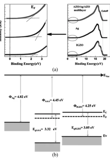
Fig. 5 (a) presents a schematic energy band diagram of individually separated layers of Ag, AZO/Ag/AZO and a- IGZO. In the separated system, the work function of the Ag electrode (
Ag=4.82 eV) is higher than the electron affinity of a-IGZO (
IGZO=4.25 eV) calculated from the UPS method. The work function data are obtained from the following equation,
where , E
cutoffand E
Fare the work function, secondary electron cutoff and Fermi level, repsectively.
The work functions were determined from the positions the of Fermi level measured from the tangent line extrapolation of the onset regarding the secondary electron peak in the spectra. Therefore, when the Ag electrode is brought into direct contact with an a-IGZO channel layer, a Schottky barrier is formed with the barrier height (Φ
B) of 0.57 eV. Such a large electron affinity of the metal linear electrode (Ag, Au and Pt) causes nonlinear behaviors in the channel layer. A Schottky barrier is formed with the barrier regime of output characteristics due to the formation of electrode being brought into direct contact with the a- IGZO height Schottky-like barrier between the elctrodes and the a-IGZO films. The Ohmic contact properties can be improved by replacing elecrode materials and/or by
Fig. 4. Transfer characteristics of the a-IGZO TFT with a W/L = 400/50 µm. The inset indicates the IDS1/2- VGSat VDS= 10 V.
SS =∂V
GS/∂( logI
DS) (2)
R
T= V
DS/ I
DS= r
chL + R
SD(3)
= h ν ( 21.2 eV ) - E
cutoff+
xE
F(4)
modifying the contact area. The therminoic emission current J is formed by electrons overcoming the Schottky barrier by the thermal energy from the metal to the a-IGZO channel layer.
where A*, T, k
B, n, and Φ
Bare the Richardson constant, temperature, ideality factor, the Boltzmann's constant, and Schottky barrier height, respectively.
The property of contacts on the a-IGZO layer depends on the Schottky barrier height [12]. When the AZO/Ag/
AZO mutilayer with the barrier height (Φ
B) of 0.02 eV is used as source/drain contacts, we focused our interest on using a heavily doped layer as a contact to source/drain because it is the conventional technology for oxide semiconductor devices. It also allows ohmic contacts, and in oxide-based semiconductors, it reduces the possibility of forming an oxide barrier at the interface, thus reducing the probability of forming an undesirable Schottky barrier [13].
4. CONCLUSIONS
In summary, the electrical properties were observed to be significantly improved for the IGZO with AZO/Ag/AZO to the Ag electrode. Our results suggest that the AZO/Ag/AZO multilayer is one of promising transparent conducting electrodes to attain better performance of IGZO based TFTs in terms of both electrical and optical aspects.
ACKNOWLEDGMENT
This work was support by both KIST Future Resource Program (2E24011) and the Converging Research Center Program through the National Research Foundation of Korea (NRF) funded by the Ministry of Education, Science, and Technology (grant number 2012K001283).
REFERENCES
[1] K. Nomura, H. Ohta, A. Takagi, T. Kamiya, M. Hirano, and H. Hosono, “Room-temperature fabrication of transparent flexible thin-film transistors using amor- phous oxide semiconductors”, Nature, Vol. 432, pp.
488-492, 2004.
[2] K. Nomura, A. Takagi, T. Kamiya, H. Ohta, M. Hirano, and H. Hosono, “Amorphous oxide semiconductors for high-performance flexible thin-film transistors”, Jpn. J.
Appl. Phys., Vol. 45, pp. 4303-4308, 2006.
[3] S.-H. K. Park, C.-S. Hwang, M. Ryu, S. Yang, C.
Byun, J. Shin, J.-I. Lee, K. Lee, M. S. Oh, and S. Im,
“Trans-parent and photo-stable ZnO thin-film transistors to drive an active matrix organic-light- emitting-diode display panel”, Adv. Mater., Vol. 21, pp.
678-682, 2009.
[4] H. Yabuta, M. Sano, K. Abe, T. Aiba, T. Den, H.
Kumomi, K. Nomura, T. Kamiya, and H. Hosono,
“High-mobility thin-film transistor with amorphous InGaZnO
4channel Fabricated by room temperature rf- magnetron sputtering”, Appl. Phys. Lett., Vol. 89, p.
112123, 2006.
[5] J.-S. Park, J. K. Jeong, Y.-G. Mo, H. D. Kim, and S.-I.
Kim,“Improvements in the device characteristics of amorphous indium gallium zinc oxide thin-film transistors by Ar plasma treatment”, Appl. Phys. Lett., Vol. 90, p. 262106, 2007.
[6] P. Barquinha, A. M. Vila, G. GonCalves, L. Pereira, R.
J = A*T2exp (-qΦB / kBT )[ exp(-qV/ nkBT )]-1(5)
Fig. 5. (a) UPS spectra of the AZO/Ag/AZO films, Ag, and IGZO film surface. (b) Schematic energy band diagram in separated systems.