P1-15 / Y. H. Eom
• IMID 2009 DIGEST
Abstract
Octadecyltrichlorosilane (OTS) self-assembled monolayer was selectively patterned by deep ultraviolet exposure, resulting in differential surface state, hydrophilic area with OTS hydrophobic surroundings. High-resolution (<10 μm) nanoparticulate Ag electrodes and organic semiconductors were patterned from simple dip-casting and ink-jetting on the pre-patterned hydrophilic surface, forming all solution-processed organic thin film transistors. The devices typically have shown a mobility of 0.065 cm2/V·s and on-off current ratio of 8 X 10⁵.
1. Introduction
C
urrently organic thin-film transistors (OTFTs) have been researched as electronic devices for diverse industrial fields such as displays and RFID [1,2]. The performances of OTFTs has been improved over the past several years and recently have shown almost equals or better than that of hydrogenated amorphous silicon thin film transistors [3].So far most of OTFTs have used gold (Au) for source and drain electrodes that were deposited at vacuum conditions. It was difficult to make low-cost and roll-to-roll process because that was needed high vacuum system such as sputter or evaporator. Moreover it takes a long time for the high vacuum conditions. Although some researchers have demonstrated micro-contact printed Au or other metal electrodes for the low-cost fabrication process [4,5], adopting them to roll-to-roll process directly is still problematic.
In this report, we demonstrated simply printed Ag electrodes by using surface treatment and dip-coating
process, which may enable to roll-to-roll process. The OTFTs fabricated with the solution-processed and patterned Ag nanoparticulate source/drain electrode typically have shown a mobility > 0.065 cm2/V·s.
2. Experimental
H
eavily doped p-type silicon wafer and thermally grown SiO2 (200 nm) were used as a common gateelectrode and a gate dielectric, respectively. Wafers were cleaned in the acetone, isopropylalchol, de ionized-water by sonication respectively. Then UV exposure was carried out to remove residual organic material. Octadecyltrichlorosilane (OTS) molecule was formed on the silicon oxide to create uniform hydrophobic self-assembled monolayer (SAM) [6]. OTS SAM was formed by dipping in a 30 mM hexane solution for 1 hour. After forming the OTS monolayer, deep ultraviolet (DUV) exposure was performed in nitrogen atmosphere with quartz mask, resulting in diverted hydrophilic region from hydrophobic region.
Finally, the substrate including differential surface states were dipped into Ag ink and pulled out with a withdrawal speed of 50 mm/min. Fig. 1. shows a schematic diagram of process flow of the non-relief lithography patterning process. After forming high-resolution nanoparticulate Ag electrodes (< 10 μm), the electrodes were baked at 160 ℃ for 1 hour, showing thickness of about 1500 Å and sheet resistance of 1.69 Ω/□.
All printed organic thin film transistors with high-resolution
patterned Ag nanoparticulate electrode using non-relief
pattern lithography
You Hyun Eom
1,2, Sung Kyu Park
1, Yong-Hoon Kim
1, JungWon Kang
2,
and Jeong-In Han
11
Information Display Research Center, Korea Electronics Technology Institute, Seongnam, Gyeonggi, 463-816, Korea
Phone: +82-31-789-7410 , E-mail: [email protected]
2
College of Electronics and Electrical Engineering, Dankook University,
Yongin, Gyeonggi, 448-701, Korea
P1-15 / Y. H. Eom
IMID 2009 DIGEST •
SiO2 Si wafer
DUV (Deep UV)
OTS Self Assembly Monolayer SiO2
Si wafer
OTS Self Assembly Monolayer Quartz mask
Hydrophilic region Si wafer
DUV (Deep UV)
SiO2 SiO2
Si wafer
Ag ink wetted at the hydrophilic region SiO2
Si wafer
DUV (Deep UV)
OTS Self Assembly Monolayer SiO2
Si wafer
OTS Self Assembly Monolayer Quartz mask
Hydrophilic region Si wafer
DUV (Deep UV)
SiO2 SiO2
Si wafer
Ag ink wetted at the hydrophilic region
SiO2 Si wafer
Ag ink wetted at the hydrophilic region
Fig.1. Schematic diagrams of the non-relief lithography patterning process.
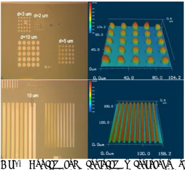
Figure 2. shows the high-resolution patterned Ag electrodes optical and confocal micrographs which is located in left side and right side, respectively. The active semiconductor layer was deposited from 2 wt% 6,13-bis(triisopropylsilylethynyl) (TIPS)-pentacene solutions in chlorobenzene, which was deposited by using ink-jet printing system (Unijet, UJ2100).
Fig.2. Optical and confocal micrographs of patterned nanoparticulate Ag electrodes from dip-casting.
3. Results and discussion
F
or a comparison, conventional bottom contact OTFTs was fabricated with photolithographically patterned (lift-off) Au source and drain (S/D)electrodes on the heavily doped silicon wafer.
Figure 3. shows optical micrographs of (a) OTFTs with non-relief lithography patterned and dip-cast nanoparticulate Ag source/drain electrodes with ink-jetted TIPS organic semiconductor, and (b) OTFTs with photolithographically defined Au source/drain electrodes with ink-jetted TIPS organic semiconductor. The device had channel length of 20 μm and width of 100 μm.
Fig.3. Optical micrographs of ink-jetted TIPS organic semiconductor onto (a) OTFTs with Ag S/D electrode (b) OTFTs with Au S/D electrode.
Figure 4 (a) and (b) show the log IDS-VGS and √IDS
-VGS curves of an OTFTs device with the
nanoparticulate Ag source/drain electrode and Au source/drain electrode.
As shown in Fig.4, electrical performance of OTFT based on the Ag electrodes typically have shown similar or slightly decreased mobility (mobility of 0.065 cm2/V·s) compared to that of OTFT with the Au S/D electrode (mobility of 0.075 cm2/V·s). Electrical characteristics of OTFT with Ag and Au S/D electrodes were summarized in Table 1.
Although we demonstrated OTFTs which were fabricated by surface pattering method on oxidized wafer, it is possible to apply the methods on polymeric substance for flexible device [7]. For using the non-relief pattern lithography technique to flexible OTFTs, there may be some problems such as poor adhesion of silane group on polymeric substance and non-uniform SAM layer. In order to fabricate the surface patterned flexible device, novel gate dielectric material may be needed to solve the problems. Poly-4-vinylphenol (PVP) was one of the well known polymer dielectric material, but it may be unable to use with non-relief pattern lithography because PVP has not enough hydroxyl groups which give a linkage with silane
P1-15 / Y. H. Eom
• IMID 2009 DIGEST
groups of OTS. To solve this problem, several novel dielectric materials and silane composites are researching for reliable non-relief-patterning lithography on polymeric substance.
Fig.4. Log IDS–VGS and √IDS–VGS curves of an
OTFTs device with a (a) Ag S/D electrode and (b) Au S/D electrode.
Table1. Electrical characteristics of OTFT with Ag and Au S/D electrode.
S/D electrode Ag electrode Au electrode
Vth (V) 10 V -2 V
S.S (V/dec) 1 V/dec 2 V/dec Ion/Ioff 8 X 10⁵ 2 X 10⁶ Mobility
(cm2/V·s) 0.065 0.075
Summary
U
sing a simple surface patterning and dip-casting, we have fabricated reproductive all solution-processed OTFTs with non-relief-patterning lithography patterned source/drain electrodes. Also we have demonstrated all printed OTFTs with high-resolution patterning process.4. References
1. R. Rotzoll, S. Mohapatra, V. Olariu, R. Wenz, M. Grigas, K.Dimmler, O. Shchekin, A. Dodabalapur,
Appl. Phys. Lett., 88, 123502 (2006)
2. L. Zhou, A. Wanga, S.-C. Wu, J. Sun, S. Park, T. N. Jackson, Appl. Phys. Lett., 88, 083502 (2006) 3. S. K. Park, T. N. Jackson, J. E. Anthony, D. A.
Mouret, Appl. Phys. Lett ., 91, 063514 (2007). 4. B.K. Choo, J.S. Choi, G.H. Kim, S.H. Lee, K.C.
Park, J. Jang, The Kor.Vac.Soc,, v15n4p354 (2006). 5. J.P. Hong, A.Y. Park, S.H. Lee, J.H. Kang, N.Y.
Shin, and Do Y.Yoon, Appl. Phys. Lett., 92, 143311 (2008).
6. S. K. Park, D. A. Mourey, S. Subramanian, J. E. Anthony, and T. N. Jackson, Adv. Mater., 20, 4145 (2008)
7. T. Minari, M. Kano, T. Miyadera, S.-D. Wang, Y. Aoyagi, K. Tsukagoshi, Appl. Phys. Lett., 94, 093307 (2009)