P1-8 / W.-S. Kim
• IMID 2009 DIGEST
Abstract
In this paper, we investigated the effects of different source/drain (S/D) electrode materials in thin film transistors (TFTs) based on indium-gallium-zinc oxide (IGZO) semiconductor. A transfer length and effective resistances between S/D electrodes and amorphous IGZO thin-film transistors were examined. Intrinsic TFT parameters were extracted by the transmission line method (TLM) using a series of TFTs with different channel lengths measured at a low drain voltage. The TFTs fabricated with Cu S/D electrodes showed the lowest contact resistance and transfer length indicating good ohmic characteristics, and good transfer characteristics with a field-effect mobility (μFE) of 10.0
cm2/Vs.
1. Introduction
Thin film transistors (TFTs) based on amorphous oxide semiconductors (AOSs) have emerged as a promising technology, particularly for active-matrix TFT-based backplanes, due to their superior electrical performance when compared with conventional amorphous silicon and polycrystalline silicon TFTs. Among the various AOSs, amorphous indium gallium zinc oxide (a-IGZO) has attracted attention since improvement in deposition techniques have made it possible to make high-quality a-IGZO thin films. A-IGZO thin films have several advantages over TFTs using channel layers of a-Si or other oxide semiconductors. Specifically, A-IGZO TFTs have high field-effect mobilities exceeding that of a-Si by a factor of 102, a small subthreshold swing, good uniformity attributed to the amorphous structure, a low off current, good stability under electrical stress, and can be processed at low temperatures.
Various reports have been published wherein oxide
semiconducting thin films were used as active channel layers in TFTs.1-3 Moreover, several research groups have already presented a-IGZO based working devices with remarkable electrical and optical properties.4,5 We have recently demonstrated high performance a-IGZO TFTs which exhibited a depletion mode where the TFT turn-on voltage (VON), on-off current ratio and field effect mobility (μFE) were 8 V, 107 and 9.21 cm2/Vs, respectively.6
Despite recent successes, some outstanding issues related to a-IGZO TFT electrical performance still remain to be resolved, such as obtaining good electrical contact between source/drain (S/D) electrodes and the semiconductor layer, addressing instabilities which occur during light illumination and operation under various environmental changes. Barquinha et al.7 showed that various S/D electrodes affected the drain current of TFTs and that an annealing process improved the electrical properties. J. Park et al.8 investigated the effects of S/D series resistance and transfer length on a-IGZO TFTs.
We focus here on an investigation of different S/D electrodes in a-IGZO based TFTs for better ohmic characteristics. The TFT S/D series resistance, the intrinsic field effect mobility (μFE-i), transfer length (LT), and effective contact resistance (RC-eff) were extracted by the well-known transmission line method (TLM) using a series of TFTs with different channel lengths. Intrinsic a-IGZO parameters are representative of the electrical characteristics of the conduction channel itself without the influence of the parasitic series resistance.
2. Experimental
Figure 1 shows a cross-sectional schematic of a
Investigation of contact resistance between metal
electrodes and amorphous gallium indium zinc oxide
(a-GIZO) thin-film transistors
Woong-Sun Kim, Yeon-Keon Moon, Sih Lee, Byung-Woo Kang, Tae-Seok
Kwon, Kyung-Taek Kim, and Jong-Wan Park*
Department of Materials Science and Engineering, Hanyang University, 17 Haengdang-dong, Seoungdong-ku, Seoul 133-791, Korea
Tel.:82-2-2220-0386, E-mail: *[email protected]
Keywords: amorphous oxide semiconductors (AOSs), thin film transistors (TFTs) a-IGZO, contact resistance, transmission line method (TLM),
P1-8 / W.-S. Kim
IMID 2009 DIGEST • Fig. 1. Cross-sectional schematic of a
bottom-gate-type a-IGZO TFT with staggered structure.
bottom-gate-type a-IGZO TFT with staggered structure. The SiNx/n-Si substrates were ultrasonically cleaned in acetone and methanol and rinsed in de-ionized water for 10 minutes each. Thin films of a-IGZO (80-nm-thick) were deposited using DC magnetron sputtering with sintered InGaZnO4 (99.999 %, purity) as the target material. Sputtering was performed at substrate temperature of 100 oC in an argon atmosphere with an oxygen partial pressure of 6%. A 4 inch diameter ceramic target, 4 cm from the substrate was used at, at a base pressure of 2.7 × 10⁻⁴ Pa, a working pressure (Ar+O
2) of 6.6 × 10⁻¹ Pa, and a plasma discharge power density of 0.5 W/cm2. An Al, Cu and Ti electrodes were used for the S/D electrodes, and these were deposited by DC magnetron sputtering at room temperature. The channel layer and S/D electrodes were defined using a lift off process, and the resulting transistors had a fixed width (W) of 100 μm, whereas the channel length (L) was varied from 10 to 50 μm. No annealing was carried out during and postdeposition of IGZO. All electrical characterizations were carried out with a semiconductor parameter analyzer (Agilent HP 4145B) at room temperature in the dark.
3. Results and discussion
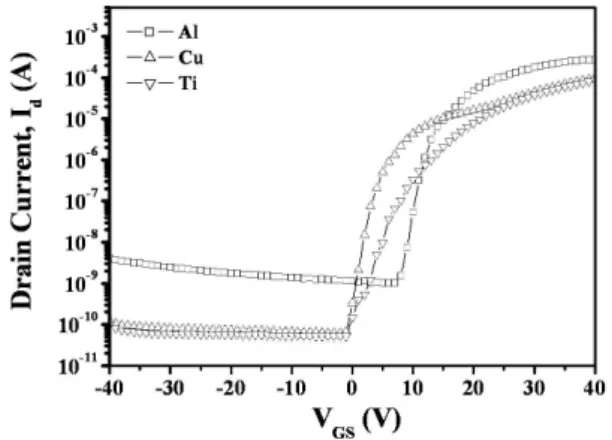
The transfer characteristics of a-IGZO based TFTs with different S/D electrodes are shown in Fig. 2 for devices with L=50 μm and W=100 μm, measured at drain-to-source voltages (VDS) of 10 V. The VON shift was shown in Fig. 3, which is considerably more positive for Al electrodes. This could be related to the formation of unintentional interfacial layer, like AlOx, and this could be pushing VON toward more positive value.7 The relatively large off-current for Al electrodes could be related to the fact that device processing was not optimized. The TFT characteristics including a field effect mobility in the linear region (μFE), a saturation region mobility (μSAT), ION/IOFF ratio,
Fig. 2. Transfer characteristics of a-IGZO TFTs with different S/D electrodes: ITO, Al, and Cu. Devices with W/L = 100/50 μm and VDS = 10 V.
a turn-on voltage (VON), a threshold voltage (Vth), and a subthreshold slope (S) with different S/D electrodes are shown in Table 1.
TABLE 1. Comparison of the electrical properties of with different source/drain electrodes : Al, Cu, ITO, and Ti including µFE, µSAT, ION/IOFF, VON, Vth
and S.
Here, the TLM was adopted to evaluate the contact resistance of different electrodes. By defining the total TFT ON resistance (RT) as RT = VDS/IDS, RT can be expressed as : D S ch DS DS T
r
L
R
I
V
R
=
=
+
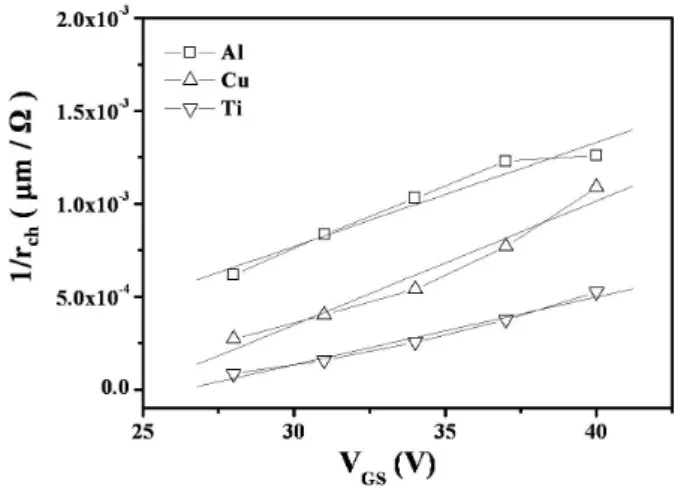
/ (1) with rch = 1/μFE-iCoxW(VGS-Vth-i), where rch is the channel resistance per unit channel length, RS/D is the series resistance at the S/D contacts, μFE-i is the intrinsic field effect mobility, Vth-i is the intrinsic threshold voltage, COX is the gate-insulator capacitance per unit area.As illustrated in Fig. 3, we plotted the total ON resistance as a function of channel length for different gate voltages, and then fitted the experimental values with linear curves for each VGS. This allowed us obtain the TFT total series resistance (RS/D) from the intercept with the y-axis, and rch from the slope. By
P1-8 / W.-S. Kim
• IMID 2009 DIGEST
Fig. 3. The total TFT ON resistance as a function of the TFT channel length for different VGS values for
an a-IGZO TFTs with Ti electrodes.
plotting the reciprocal of rch as a function of VGS and fitting the results with a line, the x-intercept gives a Vth-i, while the slope yields a μFE-i, as shown in Fig. 4. The TFTs with the Al, Cu, and Ti S/D electrodes had a μFE-i of 8.4 cm2/Vs, 10.0 cm2/Vs, and 5.5 cm2/Vs, respectively. It has been reported that the plot of RT versus L has an intersection point indicating both a resistance limit (R0) and transfer length difference (ΔL). For a-Si:H TFTs, ΔL is usually extracted from the intersection point of RT versus L curves, which is the difference between the effective channel length and the physical channel length, and are independent of the gate voltage. However, in this work, an intersection point at all gate voltages was not found because a-IGZO TFTs do not have highly doped ohmic layers.8 Therefore, the physical meaning of the transfer length, LT, is equivalent to that of ΔL. We can calculate LT numerically9, but if d / LT >> 1, the expression for LT can be reduced to:
ch D S T
r
R
L
2
/=
(2) where d is the gate to source or drain overlap distance.To evaluate the performance of different S/D electrodes more precisely, we need to define the effective contact resistance (RC-eff), which represents the effective contact area. TFT drain current does not flow through the whole contact area but is more likely limited to a specific area of contact. This RC-eff has to be as small as possible because the contact area yields
Fig. 4. Reciprocal channel resistance per unit length (1/rch) extracted from Fig. 3 as a function of
VGS.
an increase in the TFT parasitic capacitances that can degrade device operation. RC-eff is defined as the sum of the contact resistivity and the bulk resistivity associated with the access area and can be calculated from LT as: ch T eff C WL r R = 2 − (3) Figure 5 shows the variation of RS/D, rch, LT and R C-eff with VGS calculated from the experimental results for Al, Cu, and Ti S/D electrodes. As VGS increased, RS/D, rch, LT and RC-eff decreased for all electrodes. It is considered that the RS/D is dependent on rch, because RS/D is affected by the interface properties between channel layer and S/D electrode, which are mainly controlled by the VGS. The lowest RC-eff was observed for the case of the Cu electrode. We can approximate RS/D using RC-eff where the horizontal resistivity is assumed to be negligible compared to vertical resistivity at high VGS.9 This RC-eff value is smaller than the RS/D estimated using a contact area approximation. Therefore, the vertical current flow at the contact area is effectively confined within the characteristic length, LT. For a-Si:H TFTs, the total resistance is affected by the highly doped ohmic layer properties. However, for a-IGZO TFTs, the total resistance is influenced by the interface properties between channel layer and S/D electrodes. Therefore, the RS/D is more dependent on total resistance and the choice of the S/D electrode is more important, requiring a material like Cu which has low resistance, a smooth interface, and good ohmic contact. The LT
P1-8 / W.-S. Kim
IMID 2009 DIGEST • Fig. 5. Plot of channel resistance (rch), total S/D
contact resistance (RS/D), calculated effective
contact resistance (RC-eff) and characteristic length
(LT) as a function of VGS.
value obtained in this letter is much larger than those extracted in previous reports.8,9 This large L
T value seems to be caused by our device structure, i.e., bottom gate staggered type having a whole-area gate electrode. There are no gate-to-source or gate-to-drain area overlapping distance effects. Also, a relatively low rch could be related to this structure. Therefore, the value of RC-eff may be acceptable although the LT value is comparatively large. The decrease in the rate of RC-eff may be affected by the RS/D decrease because LT decreases slightly, while the RS/D decreases continuously. From these results, for a Cu electrode, a very low RC-eff is shown, which is adequate for a-IGZO TFTs.
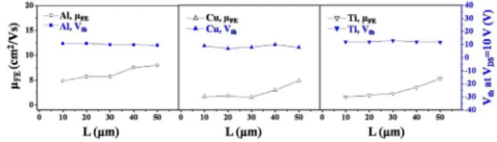
The obtained μFE and Vth are shown in Fig. 6 as a function of channel length. In all the case of different electrodes, μFE increases as L increases. This means that RS/D should not significantly influence μFE as compared with the channel resistance and, thus, μFE will mostly depend on channel resistance. As channel length increases, the contribution of RS/D in RT decreases, and the voltage drop is negligible at the contact resistance. Thus, μFE value increases for μFE-i values with long channels.
4. Summary
To investigate the effects of contact resistance on the characteristics of a-IGZO TFTs, bottom gate staggered-type TFTs were fabricated using Al, Cu, and Ti S/D electrodes. Since a-IGZO TFTs do not have a highly ohmic layer, the ΔL could not be found, and LT
Fig. 6. The field effect mobilities and threshold voltage as a function of the TFT channel length for a-IGZO TFTs with ITO, Al, and Cu S/D electrodes.
was calculated numerically. The TFT with the Cu electrodes had a field-effect mobility (μFE) of 4.8 cm2/Vs, an intrinsic field-effect mobility (μFE-i) of 10.0 cm2/Vs and an effective contact resistance (RC-eff) of 0.005 Ω/cm2. Consequently, the results in this work indicate that RC-eff works as a series resistance to deteriorate the TFT performance, and that replacement of ITO S/D electrodes in a-IGZO TFTs can be realized by employing electrodes with a smaller RC-eff, such as Cu. Further investigations relating to the S/D ohmic contact quality, interfacial layer formation, and instability of various S/D materials are desired for TFTs based on amorphous oxide semiconductors to reduce the contribution of S/D series resistance to the total resistance.
5. References
1. R. L. Hoffman, B. J. Norris, and J. F. Wager, Appl. Phys. Lett., 82, 733 (2003).
2. H. Wu, J. Liang, G. Jin, Y. Lao, and T. Xu, IEEE Trans. Electron Devices, 54, 2856 (2007).
3. R. Martin, P. Barquinha, I. Ferreira, L. Pereira, G. Goncalves, and E. Fortunato, J. Appl. Phys., 101, 044505 (2007).
4. H. Kumomi, K. Nomura, T. Kamiya and H. Hosono, Thin Solid Films, 516, 1516 (2008).
5. K. Nomura, A. Takagi, T. Kamiya, H. Ohta, M. Hirano and H. Hosono, Jpn. J. Appl. Phys., 45, 4303 (2006).
6. Y. K. Moon, S. Lee, and J. W. Park, J. Korean Phys. Soc., 51, 412 (2008).
7. P. Barquinha, A. M. Vilà, G. Gonçalves, L. Pereira, R. Martins, J. R. Morante, and E. Fortunato, IEEE Trans. Electron Devices, 55, 954 (2008)
8. J. Park, C. Kim, S. Kim, I. Song, S. Kim, D. Kang, H. Lim, H. Yin, R. Jung, E. Lee, J. Lee, K.W. Kwon, Y. Park, IEEE Electron Device Lett., 29, 879 (2008)
9. C. S. Chiang, S. Martin, J. Kanicki, Y. Ugai, T. Yukawa, and S. Takeuchi, Jpn. J. Appl. Phys., 37, 5914 (1998)