용액공정에 의한 Indium Gallium Oxide (IGO)
박막 트랜지스터 제작
Fabrication of Indium Gallium Oxide (IGO) Thin Film
Transistors by a Solution Deposition Method
Eun Jin Bae*,**, Seung Yeol Han**, Si Ok Ryu*, Chih Hung Chang**
*School of Display & Chemical Engineering, Yeungnam University, **Department of Chemical Engineering, Oregon State University
Recently, a great number of researches in the field of thin film transistor (TFT) have been performed to develop a novel oxide semiconductor having wide-band gap.(1) Various materials have been studied as candidates of the novel oxide semiconductors. Indium gallium oxide (IGO) attracts much attention as a key semiconductor for transparent TFT because of its high channel mobility and good optical transmittance. Indium gallium oxide is a wide band gap, n-type semiconductor.
Indium oxide (In2O3) and gallium oxide (Ga2O3) are semiconductors exhibiting good
transparency. Their energy band gaps are 3.7 eV for In2O3 and 4.9 eV for Ga2O3. Since In2O3 with
bixbyite structure is a very important n-type transparent semiconductor with excellent optical properties, it has been used in many areas: flat-panel displays, flexible electronics, solar cells, and so on. Ga2O3 with the monoclinic structure is considered as a promising candidate of transparent
oxide semiconductors in deep UV range.(2) IGO has both beneficial properties of In
2O3 and Ga2O3,
which has a wide band gap and is an n-type semiconductor. It is known that IGO is an alterative covalent heavy-metal cation amorphous oxide.(3) IGO has been considered as one of the promising
candidates for a new-type phase change memory (PCM) cell because it is the phase change material between the high-resistive amorphous phase and the low-resistive cubic phase.(4)
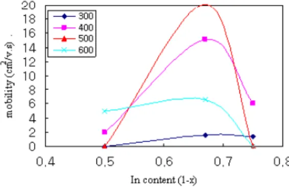
Indium gallium oxide (IGO) for thin film transistors (TFTs) were synthesized on the thermally oxidized SiO2 (100 nm thickness)/Si substrates using a solution-based deposition method. In the
synthesis, the IGO thin films were prepared in the various mole ratios of indium to gallium and they were annealed at several different temperatures. Field effect mobility (μFE) of IGO TFTs increased
with increasing the annealing temperature until 500℃. Its field-effect mobility was also changed with varying the mole ratio of indium to gallium. While the highest performance of μFE≈19.5 cm2/V∙s
was obtained at 500℃, the lowest mobility of μFE≈0.34 cm2/V∙s was obtained at 300℃ for the
annealing. On-to-off current ratio was greater than 105 and average value of their transmittance was 98% in this study. Optical band gap of thin films was varied from 3.83 eV to 4.70 eV with increasing the gallium content.
Fig. 1. The mobility of the IGO TFTs was varied with the indium content.
1. R.E. Presley, D. Hong, H.Q. Chiang, R.L. Hoffman, J.F. Wager, Solid-State Electronics 50 (2006) 500-503.
2. Fan Yang, Jin Ma, Caina Luan, Lingyi Kong, Applied Surface 255 (2009) 4401-4404. 3. H. Q. Chiang, D. Hong, C. M. Hung, R. E. Presley, John F. Wager, C.-H Park, D. A.
Keszler, G. S. Herman, J. Vac. Sci. Technol. B, 24 6 (2006) 2702-2705.
4. S.-L. Wang, C.-Y. Chen, M.-K. Hsieh, W.-C. Lee, A.H. Kung, L.-H. Pend, IEEE Xplore (2008) 33-36.