P1-3 / K. W. Lee
IMID 2009 DIGEST •
Abstract
We’ve studied the optical and electrical properties of amorphous indium gallium zinc oxide thin-film transistor (a-IGZO TFT). When the a-IGZO TFT was illuminated at a wavelength of 660 nm, the off-state drain current was slightly increased, while below 550 nm it was increased significantly. The a-IGZO TFT was extremely sensitive, with deep-level defects at approximately 2.25 eV near the midgap.
1. Introduction
Recently, many researchers have studied about zinc oxide (ZnO)-related thin-film transistors (TFTs) due to their potential as next-generation replacements for conventional TFTs. They have several interesting properties compared to amorphous Si-based TFTs, such as a direct wide band gap, good transparency, and high Hall mobility.1 With those properties,
amorphous indium gallium zinc oxide (a-IGZO) is frequently used as an active layer for the TFTs in flat-panel displays.2,3 Recently, Chuang et al.4
demonstrated that the a-IGZO TFT could detect in the visible and ultraviolet (UV) ranges. Their photosensitivity for wavelengths above 400 nm was found to be relatively low. However, Lee et al.5
reported that the solution-based IGZO TFT could detect in the visible ranges, which showed the photo sensitivity for wavelengths above 550 nm (~ 2.25eV) was found to be very sensitive relatively. Accordingly, to find light effects, we investigated the photosensitivity of a-IGZO TFT.
2. Experimental
The a-IGZO TFT was fabricated on SiO2-buffered
glass substrates. First, a 200-nm-thick MoW was sputtered onto the SiO2-buffered glass substrate, to act
as a gate metal. Then, a 200-nm-thick SiNx film was
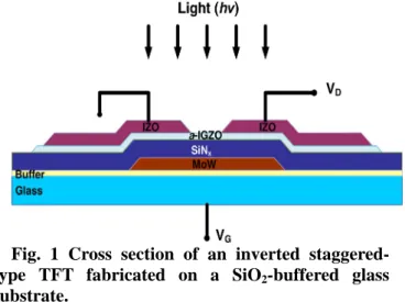
grown on the substrate by plasma-enhanced chemical vapor deposition to act as a gate dielectric. A 500-nm-thick active layer was deposited by rf magnetron sputtering of IGZO. Finally, the metal electrode was deposited by rf magnetron sputtering of indium zinc oxide (IZO). Figure 1 shows final cross section of an inverted staggered-type TFT fabricated on a SiO2
-buffered glass substrate. The performances of the a-IGZO TFT with length (L) of 150 μm and width (W) of 1000 μm were measured at room temperature (RT) with a semiconductor parameter analyzer 4156C. For illumination, a 500 W Hg (Xe) arc lamp and a monochromator were used. The optical power of the monochromatic light was measured by a UV-enhanced Si detector.
Fig. 1 Cross section of an inverted staggered-type TFT fabricated on a SiO2-buffered glass
substrate.
Light Effects of amorphous indium gallium zinc oxide thin-film
transistor
Keun Woo Lee, Hyun Soo Shin, Kon Yi Heo, Kyung Min Kim and Hyun
Jae Kim
School of Electrical and Electronic Engineering, Yonsei University, Seoul 120-749, Korea Tel.:82-2-2123-5865, E-mail: [email protected]
P1-3 / K. W. Lee
• IMID 2009 DIGEST
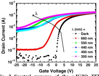
Fig. 2 Spectral response of the a-IGZO TFT observed in the log10 IDS – VG curves.
3. Results and discussion
To explore the photosensitivity over a wide detection range, we investigated the electrical properties and photosensitivity of IGZO TFT.The a-IGZO TFT behaved as an n-channel transistor and the electrical parameters were determined from a plot of
IDS1/2 vs. VG on the basis of the following relationship in the saturation regime
2 ) ( G TH sat i DS L V V C W I = ⋅ μ − (1) where IDS is the drain current, Ci is the capacitance per unit area, μsat is the field-effect mobility, and VTH is the threshold voltage. Figure 2 shows the spectral responses are plotted as log10 IDS – VG curves with VG = ± 25 V, VD of 5.0 V. They were obtained via monochromatic photon illumination from 350 nm to 660 nm wavelengths (~0.6 mW/cm2). The electrical properties of the a-IGZO TFT in the dark showed that with a μsat of approximately 8.21 cm2/Vs and a VD of 5.0 V, the current on/off ratio was approximately 8.4×10⁶, the subthreshold swing was about 0.52
V/decade, and VTH was approximately 2.2 V. Figure 3 shows the electrical characteristics of the a-IGZO TFT with VD of 5.0 V. As increasing photo energy, electrical properties of the a-IGZO TFT were changed rapidly. Under illumination, VTH shifted to lower VG values with increasing photo energy. Below 550 nm,
VTH appeared to be a large negative (below -8.0 V), indicating that the holes were trapped within the channel and/or at the interface between the channel and gate oxide. We concluded that the light with energy above 2.25 eV (550-nm wavelength) was strongly absorbed and had a strong effect on the TFT transfer characteristics, because the light generated a large density of electron-hole pairs in the device channel.
Fig. 3 Dependence of the TFT off-state drain current, on-state drain current, on-off current ratio, threshold voltage, subthreshold swing, field-effect mobility, and photosensitivity on the incident photons energy.
P1-3 / K. W. Lee
IMID 2009 DIGEST •
The states of a-IGZO TFT channel were divided into depletion and accumulation modes by variation of the gate bias. The on- and off-state drain currents usually represented the behavior of the accumulation and depletion TFT modes, respectively. For the accumulation mode, the on-state current was a little increased under illumination. However, for the depletion mode, the off-state current was significantly increased, above 4-orders of magnitude higher, compared with dark current with energy above 2.25 eV. (550-nm wavelength). However, 660 nm photons were ineffective, showing only 5.6 times higher current under dark conditions. The photo-detecting sensitivity in the depletion state became much greater than in the accumulation state, and with a wavelength of 550 nm, the off-state drain currents were saturated. The on-off current ratio, the subthreshold swing, and mobility showed a similar trend. These parameters were very sensitive above 2.25 eV (550-nm wavelength). And also, we investigated photosensitivity. The photosensitivity P of the TFTs can be approximated as6 DSdark DSdark DSillum DSdark ph I I I I I P= = − (2)
where Iph is the drain photocurrent, IDSillum is the drain current under illumination, IDSdark is the drain current in the dark. The photodetector characteristics of a-IGZO TFT has peaked value at green illumination (550-nm wavelength, 2.25 eV) and saturated at shorter wavelengths. We have explained the photo response of a-IGZO TFT using the presence of deep-level states in the middle of the band gap as we introduced the absorption of photons in the device. Recently, Chuang et al.4 suggested that the a-IGZO
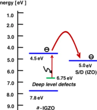
TFT was light-sensitive above 3.0 eV. The location of deep-level traps below the conduction band edge was estimated to be around 3.0 eV. However, our a-IGZO TFT were incredibly sensitive above 2.25 eV, with deep-level defects located approximately 2.25 eV near the midgap, which had shallow energy levels in the band gap, with a largely oxygen-deficient structure, compared to the a-IGZO film of Chuang et al.4 The photo-generated charge transfer and transport in the a-IGZO system can be understood from the energy diagram shown in Figure 4. During illumination, electron-hole pairs are generated in the active layer and electron transfer is possible through the a-IGZO. Electrons are injected from the deep-level traps of a-IGZO to conduction band of a-a-IGZO, and then collected by the IZO contact.
Fig. 4 Energy level diagram adjusted in relation to the vacuum level for the a-IGZO device.
4. Summary
In conclusion, we have studied the optical and electrical characteristics of the a-IGZO TFT as a function of wavelength. We found that a much higher photosensitivity was achieved when the depletion state of the a-IGZO TFT channel was applied. At photon energies higher than 2.25 eV, our TFT displayed a high photocurrent, because the related photodetection was associated with the band gap and deep-level states of the a-IGZO film. This study indicates how the a-IGZO TFT photosensitivity could affect flat-panel displays.
Acknowledgement
This work was supported by the Korea Science and Engineering Foundation (KOSEF) grant funded by the
Korea government (MOST) (No. R0A-2007-000-10044-0 (2007)).
5. References
1. P. F. Carcia, R. S. McLean, M. H. Reilly, and G. Nunes, Jr., Appl. Phys. Lett. 82, 1117 (2003).
2. K. Nomura, H. Ohta, A. Takagi, T. Kamiya, M. Hirano, and H. Hosono, Nature 432, 4 (2004).
3. B. D. Ahn, H. S. Shin, H. J. Kim, J. S. Park, and J. K. Jeong, Appl. Phys. Lett. 93, 203506 (2008).
4. C. S. Chuang, T. C. Fung, K. Nomura, B. G. Mullins, H. P. D. Shieh, H. Hosono, and J. Kanicki, Society for information Display International Symposium, Los Angeles, May 18-23, 453 (2008). 5. K. W. Lee, K. Y. Heo, and H. J. Kim, Appl. Phys.
Lett. 94, 102112 (2009).
6. P. Bhattacharya, Semiconductor Optoelectronic