XPS와 XRD 분석을 이용한 ITO 박막의 결정성과 비정질 특성에 관한 연구
고정완 · 정보영 · 오데레사†
†청주대학교 반도체공학과
Annealing Effect with Various Ambient Conditions of ITO Thin Film
Jung Whan Ko, Bo Young Jung and Teresa Oh†
†Department of Semiconductor Engineering, Cheongju University
ABSTRACT
This study was explained the correlation between the O 1s spectra and the crystallization of ITO thin films. The crystal structure of ITO thin films changed with various annealing temperatures and annealing methods such as atmosphere or vaccum conditions. The amorphous structure observed from XRD pattern showed the O 1s spectra with 531.2 eV, and the crystal structure of annealed ITO films analyzed by XRD pattern had the O 1s spectra of 529.8 eV as lower binding energy then the 531.2 eV. Oxygen in view of ITO films was related to the crystallization, and the ITO films annealed in an atmosphere pressure showed higher crystal structure than the ITO annealed in a vaccum. It was indicated that the amorphous structure had higher binding energy than the crystal structure analyzed by O 1s spectra of ITO films.
Key Words : XRD, XPS, ITO, Crystal structure, Amorphous structure
1. 서 론
TCO (Transparent Conducting Oxide)로서 주로 사용 되는 ITO(Indium Tin Oxide)는 우수한 광학적, 전기적 특성을 가지고 있는 재료[1-3]이기 때문에 FPD, LCD, OLED, touch panel, 태양전지 등의 투명전극으로서 널 리 사용되어 왔다[3-5]. ITO 박막을 상온에서 성장시킨 경우 주로 비정질 상이 얻어진다. 이는 박막이 결정성 을 가지게 하기 위한 가장 큰 요소는 열에너지이므로 상온에서 증착 된 ITO박막은 에너지를 충분히 공급받 지 못해 결정성을 갖기 어렵기 때문이다[7-8]. 일반적 으로 비정질 상의 ITO 박막보다 결정질 ITO 박막이 전기적 특성이 우수하기 때문에 결정성을 향상시키기 위한 다양한 노력이 필요하다[9-10]. ITO (indi- um tin oxide) 박막은 in에 sn을 5 ~ 10% 정도 포함한 n-type 반도체 재료로서 ITO박막을 진공 증착 할 때에 sputtering장비가 가장 많이 사용되고 있다. ITO박막은 제조방법에 따라 차이가 있지만 200 ~ 400oC이하의 온
도에서 저온공정으로 증착하여야 높은 광 투과도 와 낮은 비저항을 갖게 할 수 있으며, ITO박막을 상온에 서 성장시키게 되면 비정질 상이 나타난다[11].
ITO박막은 In2O3(indium oxide)에 SnO2(Tin oxide) 를 고용시켜 제조한 재료[6-11]로서 가시광선 영역에 서 높은 광 투과도를 가지고 적외선 영역에서는 반사 율이 크며, 그리고 자외선 영역에서는 흡수특성을 강 하게 나타낸다. 이처럼ITO박막의 특성은 사용된 증착 기술과 증착 후 열처리 기술에 따라 각각 다르게 나타 난다[1-14].
이번 실험에서 진행된 실험으로는 각각 진공과 대 기 중에서 각각 상온, 100oC, 200oC 의 조건으로 Annealing하여 그 효과를 비교하고 분석하는 실험을 해 보았다.
2. 실험방법
ITO박막의 열처리 온도와 결정구조와의 관계를 살 펴보기 위해서 산소가스 20 sccm을 주입하여 스퍼터 방법으로 박막을 증착한 뒤 열처리를 100도와 200도에
†E-mail : [email protected]
서 실시하였다. 열처리 환경은 대기 중에서와 진공 중 에서 하였으며, 박막의 분석은 XRD, XP, PL 분석방법 을 이용하였다. 전기적인 특성을 살펴보기위해서 A/
ITO/Si wafer 구조의 금속공정을 수행하여 Al 전극을 만들어서 I-V 특성을 측정하였다.
3. 실험결과 및 고찰
Fig. 1은 대기 중에서 열처리한 ITO박막의 XRD 패 턴을 보여준다. 열처리한 박막에서 XRD 패턴의 강도 가 가장 높게 나타나는 것으로부터 ITO 박막은 열처리 를 하면 결정질이 되는 것을 알 수 있다. 그러나 ITO 박 막의 결정성은 100도에서 열처리할 때 결정성이 높았으 나 200도에서 열처리를 하면 강도가 약해지고 있다.
Fig. 2는 진공 중에서 열처리한 ITO박막의 XRD 패 턴을 보여준다. 증착한 박막은 비정질특성을 나타냈으 며, 100도에서 열처리를 할 때 결정성이 가장 높았다.
반면에 200도에서 열처리를 하면 XRD 패턴의 강도가 급격히 감소하는 것을 알 수 있다.
Fig. 3은 대기 중에서 열처리한 ITO박막의 PL 스펙트 라를 보여준다. 대기 중에서 증착한 ITO박막은 540 nm 근처에서 픽이 나타나고 열처리를 하면 480 nm와 710 nm근처에서 픽이 나타나고 있다. 710 nm에서의 픽은 대기 중에 ITO 표면에서 산소와 반응하여 생긴 산소 관련된 결합 픽임을 알 수 있다.
Fig. 4는 진공 중에서 열처리한 ITO박막의 PL 스펙 트라를 보여준다. 진공 중에서 증착한 ITO박막은 540 nm근처에서 강한 결합 픽이 나타나며, 200도 열처리를 한 경우 PL 스펙트라의 강도는 가장 낮았다. 이러한 특성은 Fig. 2의 XRD 패턴에서 얻은 비정질 특성과 연관이 있음을 알 수 있다. 공통적으로 ITO 박막은 결 정질의 결합구조를 갖는 경우 PL의 강도가 높게 나타 났다.
Fig. 5는 대기 중에서 열처리한 ITO박막의 XPS 스
Fig. 1. XRD patterns of ITO thin films after annealing process in an atmosphere pressure.
Fig. 2. XRD patterns of ITO thin films after annealing process in a vacuum.
Fig. 3. PL spectra of ITO thin films after annealing process in an atmosphere pressure.
Fig. 4. PL spectra of ITO thin films after annealing process in a vacuum.
펙트라를 보여준다. 대기 중에서 열처리를 함에 따라서 O 1s 스펙트라는 화학적 이동을 나타나고 있으며, 열 처리 온도가 높을수록 낮은 결합에너지쪽으로 이동하 고 있다. 낮은 결합에너지로의 이동은 ITO박막을 구성 하고 있는 원자들 간의 결합력이 약해지는 것으로서 이러한 특성은 Fig. 1에서의 XRD 데이터가 결합강도 가 낮아지는 것과 일치한다. 하지만 RT온도에서 증착 한 ITO 박막은 비정질 특성을 갖는 것으로 확인 되었 으나 O 1s 스펙트라에서는 높은 결합에너지를 갖는다.
Fig. 6은 진공 중에서 열처리한 ITO박막의 XPS 스 펙트라를 보여준다. 열처리 온도에 따른 화학적이 이동 이 관찰이 된다. 온도가 높을수록 O 1s 스펙트라가 낮 은 결합 에너지쪽으로 이동하고 있다. 100도 열처리한 ITO 박막에서 화학적 이동이 가장 컸으며, Fig. 2에서 XRD 패턴에서는 100도에서 결정성이 가장 높았으나 결합구조가 결정질로 갈수록 O 1s 스펙트라 결합에너
지 값은 가장 낮은 것을 알 수 있다. RT온도에서 증착 한 비정질 특성의 ITO 박막에서 O 1s 스펙트라 결합 에너지는 531.2 eV 으로 가장 큰 결합에너지를 갖는 것으로 나타난다.
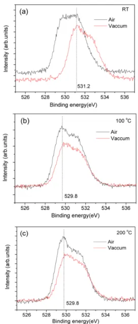
Fig. 7(a)는 상온 RT (room temperature)에서 증착한 ITO 박막의 O 1s 스펙트라를 비교하였다. 결합픽은 Fig. 5. O 1s spectra of ITO thin films after annealing
process in an atmosphere pressure.
Fig. 6. O 1s spectra of ITO thin films after annealing process in a vacuum.
Fig. 7. (a) O 1s spectra of ITO thin films at room temperatures, (b) O 1s spectra of ITO thin films depending on various annealing process at 100oC, (c) O 1s spectra of ITO thin films depending on various annealing process at 200oC.
531.2 eV으로 같은 위치를 보여준다. 따라서 비정질 특성의 ITO 박막의 O 1s 스펙트라는 결정질의 ITO 박막보다 높은 결합에너지는 갖는 것을 알 수 있다.
Fig. 7(b)와 Fig. 7(c)에서는 100도와 200도에서 열처 리한 ITO 박막의 O 1s 스펙트라를 비교하였다. 결합 픽의 위치는 529.8 eV으로 일치하였으며, 결정질 ITO 박막은 XRD 패턴의 결합강도에 상관없이 결정성을 가질 때 O 1s 스펙트라에서 결합에너지가 일정함을 보 여준다.
Fig. 8은 열처리 온도에 따른 ITO박막의 전압-전류 특성을 나타낸다. 대기 중에서 열처리한 ITO박막의 전 압-전류특성은은 온도에 상관없이 서로 비슷한 오믹특 성을 보여주었다. 따라서 ITO 박막은 투명전극으로서 의 우수한 특성을 갖는 다는 것을 알 수 있다.
ITO 박막은 열처리 환경 즉 대기 중에서 열처리효과 와 진공 중에서 열처리한 효과를 XRD, XPS, PL로 분석 해 본결과 서로 비슷한 특성을 나타냈으며, 열처리 온도 에 의하여 변화가 크게 일어나는 것을 알 수 있었다.
ITO 박막의 결정에너지는 비정질 구조일 때531.2 eV으 로 결정질일 때 결합에너지 529.8 eV 보다 크다는 것 을 확인하였다. ITO박막의 결합구조는 열처리 온도에 의한 영향이 크게 작용하고 있는 것을 확인하였다.
4. 결 론
ITO 투명전극에 대하여 물리적인 결합구조와 화학 적인 특성에 대하여 살펴보기 위하여 ITO 박막을 증착 한 뒤 열처리를 거친 샘플들을 XRD와 XPS 분석을 이 용하여 물리적 화학적 특성들을 서로 비교하였다. ITO 박막은 열처리를 하면서 결정질 구조로 변하되는 것을 확인하였으며, 열처리 방법에 따라서 결정의 강도에서
변화가 있었다. 대체로 100도에서 열처리를 하면 결정 성이 가장 높게 나타났는데 더 높은 온도에서 열처리 를 하면 열처리를 하는 방법과 무관하게 대체적으로 결정성의 강도가 줄어드는 것을 알 수 있었다. XPS 분 석을 통한O 1s 스펙트라의 주픽이 화학적 이동을 분석 한 결과, 비정질 특성일때 531.2 eV으로 결합 에너지 가 높았다. 그리고 결정질인 경우 529.8 eV으로 결합 에너지가 낮아지는 것으로 나타났다. ITO박막은 열처 리온도에 따라서 물리적, 화학적, 광학적 특성이 매우 다르게 나타났으나 전기적인 특성은 열처리온도에 상 관없이 거의 비슷한 오믹특성을 나타내는 것을 알 수 있었다.
감사의 글
이 논문은 한국산업기술진흥원의 2014년 지역기술 인재의 지역기업취업촉진을 위한 인력양성사업의 지원 을 받아 수행되었습니다.
참고문헌
1. Yasui, H. “ITO Thin films prepared by magnetron sputtering method using ITO target (Effects of plasma conditions and substrate temperature on ITO film properties)”, JSME International Journal Series B, 38 pp. 108-113, (1995).
2. Im-Young Lee, Ky-Am Lee, “Properties of indium tin oxide thin films annealed in vacuum”, Korean Jour- nal of Optics and Photonics, 11 pp. 152-157, (2000) 3. Kyo Yong Han, “Indium tin oxide (ITO) gate elec- trode deposition and low temperature annealing”, Collection of Dissertations-Research Institute for Technology Industry, 21, pp. 85-88, (1993).
4. Sung Jin Kim, Kyoon Choi, Se Young Choi, “Rapid thermal annealing effects on the electrical and struc- tural properties of ITO thin films deposited at room temperature”, Journal-Korean Institute of Metals and Materials, 51(9), pp.691-699 (2013).
5. Won-Hyo Cha, Ji-Eon Youn, Dong-Hyun Hwang, Chul-Su Lee, In-Seok Lee, Young-Guk Sona, “The electrical properties of PLZT thin films on ITO coated glass with various post-annealing tempera- ture”, Journal of the Korean Vacuum Society, 17, pp.
28-33, (2008).
6. Tae-Gyun An, Yeon-Serk Yu, “Anti-reflection and Electromagnetic wave shielding properties of the oblique angle deposited ITO films”, Collection of Dissertations-Korea Information Technology Research Fig. 8. I-V characteristics of ITO thin films after annea-
ling process in an atmosphere pressure.
Institute, 12, pp. 1-9, (2014).
7. So-Ra Kim, Jung-Eun Seo, Sang-Ho Kim, In-Seon Lee, Dong-Won Kim, “Optical and electrical proper- ties of ITO/Ni/ITO thin films”, Journal of Surface Engineering, 38, pp. 55-59, (2005).
8. Ju-Hee Heo, Dae-Sub Han, Yu-Lim Lee, Kyu-Mann Lee, In-Woo Kim, “Electrical and structural charac- teristics of ITO thin films deposited under different ambient gases”, Journal of the Semiconductor and Display Equipment Technology, 7, pp. 7-11, (2008).
9. Bong-Kun Lee, Kyu-Mann Lee, “Effect of the sur- face roughness of ITO thin films on the characteris- tics of OLED device”, Journal of the Semiconductor and Display Equipment Technology, 8, pp. 52, (2009).
10. D. R. A. Kiasatpoura, H. R. Fallaha, A. S. H. Roza- tianc, “Surface characterization and microstructure of ITO thin films at different annealing temperatures”, Applied Surface Science, 253, pp.9085–9090, (2007).
11. Hyunjung Shin, Chanhyung Kim, Changdeuck Bae, Jang-Sik Lee, Jaegab Lee, Sunghan Kim, “Effects of
ion damage on the surface of ITO films during plasma treatment”, DuPont Display, 253, pp. 8928- 8932, (2007).
12. Jiaxiang Liu, Da Wu, Shengnan Zeng, “Influence of temperature and layers on the characterization of ITO films”, Journal of Materials Processing Technology, 209, pp. 3943-3948, (2009).]
13. Huei-Tzong Lu, Meiso Yokoyama, “Plasma prepara- tion on indium-tin-oxide anode surface for organic light emitting diodes”, Journal of Crystal Growth, 260, pp. 186-190, (2004).
14. G. Kavei, A. M. Gheidari, “The effects of surface roughness and nanostructure on the properties of indium tin oxide (ITO) designated for novel optoelec- tronic devices fabrication”, Journal of Materials Pro- cessing Technology, 208, pp. 514-519, (2008).
접수일: 2015년 10월 19일, 심사일: 2015년 11월 4일, 게재확정일: 2015년 11월 30일