P2-56 / K-B Yoon
• IMID 2009 DIGEST
Abstract
The effect of different annealing methods on the sheet resistance of indium tin oxide (ITO) on polyimide (PI) substrate has been investigated. As electro-annealing induced the predominant growth of crystallites of ITO thin films along (4 0 0) plane, the sheet resistance of ITO films that were electro-annealed for 2 mA at 180 ℃ considerably decreased from 50 to 28 Ω/cm2.
1. Introduction
Transparent polymer substrates offer substantial advantages in terms of being able to develop displays that are thinner, lighter, more robust, deformable and can be rolled up when not in use. The ITO thin films that were deposited on polymer substrates, however, showed a high level of electrical resistance because substrate heating is limited due to its low thermal stability. As a result, polymer substrates with high glass transition temperature have been mainly investigated for their resistance to higher temperature during deposition [1,2].
Also, annealing experiments of ITO thin films on polymer substrates have been implemented and several researches confirmed that annealing temperature affects the microstructure, electrical and optical properties of ITO thin films [3,4].
A detailed investigation of the electrical and optical properties of ITO thin films on polymer substrates after electro-annealing, however, has not been conducted. In this paper, we have investigated the electrical and optical properties of ITO thin films on polyimide substrates as a function of electro-annealing conditions. The effect of electro-annealing on the microstructures and sheet resistance of the ITO thin films was investigated.
2. Experimental
A commercial colorless polyimide (PI, Mitsubishi Gas Chemical, Neopulim-L), that has thickness of
200±10 µm, surface roughness of 1 nm and Tg of
300 was used as a substrate for the deposition of ℃ ITO films. ITO thin films were prepared by RF magnetron sputtering of an oxide ceramic target (In2O3/SnO2 = 90/10 wt%) at room temperature. The
temperature of PI substrate rose up to 60 during℃
sputtering. The distance from target to substrate was
100 mm. A base pressure below 5.0×10⁻⁶ Torr was
maintained prior to the deposition. High purity Ar was used as the sputtering gas and the process pressure was kept at 2.1×10⁻³ Torr.
ITO films that had thickness of 280 nm were obtained at 75 W for 20 min at room temperature and these factors were used for all experiments. The electro-annealing of the ITO thin films was conducted at a constant current flow (2 mA), which was heated from 100 to 180 for 6℃ 0 min and cooled in ambient to room temperature conditions in air. Thermal annealing was carried out in the same manner was that of electro-annealing.
The microstructure of the ITO thin films was investigated by X-ray diffractometer (Phillips X’Pert
APD) with CuKα (1.5418 ) radiation. Sheet Å
resistance was measured using a four-point probe (Mitsubishi Chemical, MCP-T610). The optical transmittance was observed using a UV–vis spectrometer (Jasco V-650). Field emission scanning electron microscope (HITACHI, S-4300) was used to observe the surface morphology and cross-sectional views of the ITO thin films.
The effect of electro-annealing on the electrical properties
of ITO film on colorless polyimide substrate
Juncheol Song, Deok-Hun Park, Insung Park, Shang-hun Shim and
Keun-Byoung Yoon*
Dept. of Polymer Science, Kyungpook National University, Daegu 702-701, Korea Tel.:82-53-950-7588, E-mail: [email protected]
P2-56 / K-B Yoon
IMID 2009 DIGEST •
3. Results and discussion
ITO-coated PI films were prepared at room temperature and annealed by electro- and thermal methods. The effect of annealing on the sheet resistance, microstructure and transmittance of the ITO-coated PI films were investigated. The sheet resistance of the annealed ITO thin films, as a function of annealing temperature, is plotted in Fig. 1.
The sheet resistance of the electro-annealed ITO thin films was slightly lower than that of thermal annealed ones at the same temperature. The sheet resistance of the annealed ITO thin films sharply
decreased from 50 to 28 Ω/cm2 with increasing the
annealing temperature. Because of the ITO film was crystallized uniformly and the crystalline ITO was enlarged at high annealing temperature. As a result, the sheet resistance or ITO films decreased in correlation with the growth of crystalline.
Through the X-ray diffraction patterns of ITO thin
films which were both annealed and non-annealed were analyzed the intensity ratio of the (4 0 0) to (2 2 2) planes, I4 0 0 / I2 2 2, as a function of the annealing
temperature, is shown in Table 1. The grain size was derived from the XRD spectra following Debye– Scheerer’s method [5], and the results are summarized in Table 1.
The intensity of (2 2 2) plane diffraction peak was higher than that for other planes in all films. The electroand thermal annealed ITO thin films are made of polycrystalline with a preferential orientation along (2 2 2) plane. Also, annealed ITO thin films were oriented along (4 0 0) plane. The sheet resistance of
Fig. 1. Changes in sheet resistance after annealing at various temperatures (deposition condition: 75 W; RT: 20 min).
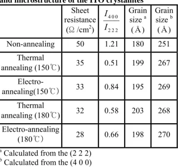
TABLE 1. Effect of annealing the sheet resistance and microstructure of the ITO crystallites
Sheet resistance (Ω /cm2) 2 2 2 0 0 4
I
I
Grain size a (Å) Grain size b (Å) Non-annealing 50 1.21 180 251 Thermal annealing (150℃) 35 0.51 199 267 Electro-annealing(150℃) 33 0.84 195 269 Thermal annealing (180℃) 32 0.58 203 268 Electro-annealing (180℃) 28 0.66 198 270a Calculated from the (2 2 2) b Calculated from the (4 0 0)
the electro-annealed ITO thin films was slightly lower than that of the thermal annealed ones at the same temperature, because the electro-annealed ITO thin films were more oriented along (4 0 0) plane.
The intensity ratio of the (4 0 0) to (2 2 2) planes (I4 0 0 / I2 2 2) was used to evaluate the annealing effect on
the crystalline texture of ITO films. The values of I4 0 0
/ I2 2 2 decreased after electro- and thermal annealing.
It is well documented that (2 2 2) plane of the crystalline ITO was predominantly enlarged due to thermal annealing and the sheet resistance of the ITO films depends upon the orientation of (4 0 0) plane rather than that of (2 2 2) plane. The I4 0 0 / I2 2 2 of the
thermal annealed ITO films was lower than that of the electro-annealed ITO films. The thermal annealed ITO films were predominantly oriented along (2 2 2) plane. Whereas the crystallites of the electro-annealed ITO films grew along (4 0 0) plane, the sheet resistance of the electro-annealed ITO films was lower than that of the thermal annealed ITO films.
The grain size of the crystalline ITO was 20 and 27 nm which were calculated from (2 2 2) and (4 0 0) plane, respectively. The grain size of the electro-annealed ITO thin films is bigger than that of the thermal annealed one in (4 0 0) plane, whereas the grain size of the thermal annealed ITO thin films is bigger than that of the electro-annealed ones in (2 2 2) plane. These results correspond with the growth of crystallites and the intensity ratio of (4 0 0) to (2 2 2) planes of the ITO films by electro- and thermal annealing. The mean free path, which is a path whereby electrons can move freely in metal, is
P2-56 / K-B Yoon
• IMID 2009 DIGEST
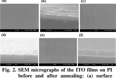
Fig. 2. SEM micrographs of the ITO films on PI before and after annealing: (a) surface morphology and (b) cross-section before annealing; (c) surface morphology and (d) cross-section after thermal annealing (at 150 ℃); (e) surface morphology and (f) cross-section after electro-annealing (at 150 ℃).
lengthened by a decrease in grain boundaries and by an induction in the decrease of sheet resistance. The increase in the grain size brings about a decrease in the grain boundaries. Sheet resistance decreases with an increase in grain size [6–8]. According to these results, electro-annealing has led to the growth of the crystallites along (4 0 0) plane and enlarged the grain size of ITO films.
In observing the changing crystalline in ITO thin films, surface morphology and cross-sections of the ITO thin films were investigated with SEM images are shown in Figure 2. The surface morphology and cross-sectional microstructure of non-annealed ITO film manifested a very smooth surface and could not be seen crystallites, however, the surface morphology of the electro- and thermal annealed ITO film (Figure 2(c) and (e)) showed microcrystalline points such as grain aggregates. The cross-section of the electro-annealed ITO film clearly showed a polycrystalline phase and grains with a columnar structure.
4. Summary
ITO thin films were deposited onto PI substrate by RF magnetron sputtering at 75 W, room temperature for 20 min. The effect of electro- and thermal
annealing on the microstructural, optical and electrical properties of ITO thin films has been investigated. Sheet resistance considerably decreased by annealing over 150 ℃. At 180 ℃, the sheet resistance of the electro-annealed ITO film showed a considerable reduction from 50 to 28 V/cm2. The electro-annealed ITO thin films increased predominant growth of crystallites of ITO films along (4 0 0) plane, on the other hand, the crystallites of the ITO films grew along (2 2 2) plane by thermal annealing. The transmittance of ITO thin films was slightly improved by electroannealing because of the enlarged grain size of the electroannealed ITO films. The electro-annealing method is quite effective in reducing the sheet resistance of ITO thin films that are coated onto PI substrate. Those of the ITO thin films that were coated onto PI films can be expected to be applied to the substrates of flexible displays.
Acknowledgement
This work was supported by the Regional Innovation Center Program(ADMRC) of the Ministry of Knowledge Economy and BK21 fellowship(2009) for Kyungpook National University Intelligent Nanocomposite Materials Project Team, Republic of Korea.
5. References
1. B. Michael, C. Christoph, Surf. Coat. Technol., 200, p.932 (2004).
2. H. Han, J.W. Mayer, T.L. Alford, J. Appl. Phys., 100, p.083715/1 (2006).
3. H. Han, J.W. Mayer, T.L. Alford, J. Appl. Phys., 99, p.123711/1 (2006).
4. T.C. Lin, S.C. Chang, C.F. Chiu, Mater. Sci. Eng. 129, p.39 (2006).
5. A.E. Hichou, A. Kachouane, J.L. Bubendorff, M. Addou, J. Ebothe, M. Troyon, A. Bougrine, Thin Solid Films, 458, p.263 (2004).
6. K.L. Chopra, I. Kaur, Thin Film Device
Applications, Plenum Press, New york, USA, p.130 (1983).
7. C.R.M. Grovenor, Microelectronic Materials,
Adam Hilger, Bristol, UK, p.197 (1989).
8. W. Wohlmuth, I. Adesida, Thin Solid Films, 479, p.223 (2005).