반도체디스플레이기술학회지 제16권 제4호(2017년 12월)
Journal of the Semiconductor & Display Technology, Vol. 16, No. 4. December 2017.
75
SnO 2 박막의 열처리 온도에 따른 CO 2 가스 반응성
오 데레사
*†
*†
청주대학교 반도체공학과CO
2Gas Responsibility of SnO
5Thin Film Depending on the Annealing Temperature
Teresa Oh
*†
*†
Division of Semiconductor, Choengju University ABSTRACTThe CO
2
gas responsibility of SnO2
thin films was researched with various annealing temperatures. SnO2
was prepared on n-type Si substrate by RF magnetron sputtering system and annealed in a vacuum condition. The bonding structure of SnO2
was changed from amorphous to crystal structure with increasing the annealing temperature, and the content of oxygen vacancy was researched the highest of the annealed at 60 ℃. The SnO2
annealed at 60 ℃ had the characteristics of the highest capacitance. The special properties of CO2
gas responsibility was found at the SnO2
thin film annealed at 60 ℃ with amorphous structure because of the combination with the oxygen vacancies and CO2
gases changed the resistivity. The amorphous structure enhanced the responsibility at the SnO2
surface and the conductivity of SnO2
thin film.Key Words : XRD, XPS, SnO
2
, CO2
, Capacitance1. 서 론
1
최근에 많이 연구되고 있는 가스 센서는 주로 금속 산 화물 반도체식 가스 센서가 있다. 금속 산화물 반도체식 가스 센서는 금속 산화물 표면에 흡착되어 있는 산소와 검출 가스의 반응을 통해 나타나는 반도체의 저항변화를 측정하는 센서이다. 인체에 유해한 환경물질인 휘발성유 기화합물 VOCs (Volatile Organic Compounds)들의 가스반응 감지시스템으로 반도체식 가스 센서가 주목을 받고 있다 [1-4]. 반도체소자로 가스반응을 일으키는 수용체로 사용 되는 물질들로 SnO
2
, ZnO, WO3
, In2
O3
, CuO 등이 알려져 있 다. 금속산화물 반도체물질은 계면접합 특성에 의하여 발 생하는 산소공공의 이온화 효과에 따라서 가스와 반응하 는 화학적 특성이 달라지고 저항이 달라져서 전기신호로† E-mail: [email protected]
바꾸어 신호처리를 하기 쉽게 되므로 의료용 기기, 광 센 서 등에서 이용되고 있다[5-9]. 산화물 반도체에서의 전도 는 열처리에 의한 산소가 빠져나간 빈자리에 음전하를 갖는 산소공공의 형성으로 이루어지고 있는데 산소가 빠 져나가면서 형성되는 결합구조의 변화에 대한 연구가 이 루어져 왔다[10-13].반도체가스 센서는 사용되는 박막은 높은 광 투과율과 높은 전자농도, 3.1eV 이상의 넓은 밴드 갭, ~10
-4
Ω㎝ 이하의 낮은 비 저항의 특성을 나타내야 한 다[14-16].본 논문에서는 SnO
2
박막을 이용하여 산소공공에 의한 산화물반도체의 전기적인 특성이 CO2
가스에 대하여 어 떻게 반응하는지를 알아보았다. CO2
가스에 대하여 반응 하는 수용체로서 SnO2
박막은 RF 마그네트론 스퍼터링 방법을 이용하여 증착하고, SnO2
박막의 결정구조를 다양 하게 바꾸기 위하여 열처리를 하였으며, 열처리에 의하여 산소공공의 함량비와 결정구조가 달라진 SnO2
박막의 전오 데레사
반도체디스플레이기술학회지 제16권 제4호, 2017 76
기적인 특성을 서로 비교하였다. I-V 특성 곡선에 의한 SnO
2
박막의 계면특성을 통하여 SnO2
박막과 기판 사이의 접촉저항이 달라짐에 따른 반도체 접합특성과 결정구조 사이의 관계를 조사하고 CO2
가스유량에 따른 전기적인 특성을 연구하였다.2. 실험방법
SnO
2
박막을 증착하기 위해서 Ar:O2
=20 sccm:20 sccm 혼합 가스를 이용하여 n-type Si 기판 위에 70 W RF파워에서 마 그네트론 스퍼터링 방법으로 증착하고 열처리를 하였다.박막 증착 후 60도, 110도, 160도와 210도에서 열처리를 진 공 중에서 실시하였다. 화학적인 특성은 XPS를 이용하여 측정하였고, 산소공공은 O 1s스펙트라를 디컨벌루션을 통 하여 얻었다. 전기적인 특성을 관찰하기 위해서 MIM (Metal-SnO
2
-Si wafer)구조의 전극을 만들어 커패시터를 제작하였다. 전기적인 특성은 I-V곡선으로 얻었으며, 미시 영역에서의 접합특성을 조사하고 접합특성과 산소공공의 연관성 그리고 결합구조에 대하여 연구하였다. SnO2
박막 의 CO2
가스반응성에 대하여 조사하기 위해서 CO2
가스 유량을 변화시켜가면서 I-V 곡선을 관찰하였다.3. 실험결과 및 고찰
Fig. 1은 SnO
2
박막의 열처리 온도에 따른 XPS 패턴이다.열처리 온도가 증가할수록 110도 이상의 온도에서 40 (2 theta) 근처에서 픽의 크기가 증가하고 있으며, 결정질 구 조로 변하고 있다. 60도에서 열처리를 하여도 비정질 구 조를 나타낸다.
Fig. 1. XRD patterns in according to the annealing temperatures of SnO
2
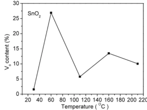
thin film.Fig. 2는 결함에너지 스펙트라로부터 디컨벌루션을 하 여 얻어진 산소공공의 함량비를 나타낸 것으로 비정질을 나타내는 60도 열처리 공정 후의 SnO
2
박막에서 산소공공 이 가장 높게 나타났다. 열처리온도가 높아지면서 박막의 밀도가 치밀해질수록 결정구조로 변해가고 있다는 것을 알 수 있다. 일반적으로는 산화물반도체의 특성이 산소공 공이 클수록 결정질이 된다고 알려져 있으나, Fig. 2의 산 소공공 함량비를 보면 산소공공의 비가 높은 곳에서 결 정질이 되지 않는 것을 알 수 있으며, 산소공공과 결정구 조는 반드시 일치하지 않는다는 것을 알 수 있다.Fig. 2. Content of oxygen vacancy in according to the annealing temperature of SnO
2
films analyzed by XPS.Fig. 3에서는 커패시턴스를 나타내며, 커패시턴스의 영 역 -5V<커패시턴스<5V 영역에서 60도 열처리한 SnO
2
박막 에서 커패시턴스 값은 낮아지고 있다. 따라서 비정질의 SnO2
박막이 전기적으로 전하가 많다는 것을 알 수 있다.Fig. 4는 열처리 온도에 따른 SnO
2
박막의 전압전류 특 성을 보여준다. 60도에서 열처리한 SnO2
박막에서 비선형 성이 가장 크게 나타났다. 열처리 온도가 높아지면서 결 정질 구조로 변하면서 전기적인 특성이 비정질 특성의 전기적인 특성과는 다르게 변하고 있다는 것을 알 수 있 다. 결정질 특성을 갖는 샘플인 110도, 160도와 210도 열처 리한 SnO2
박막들의 I-V 특성을 비교하면 열처리온도가 높을수록 전류 값이 낮아지고 있다. 즉 전하들이 줄어들 고 있다는 것을 의미한다. Fig. 2에서 산소공공의 함량이 줄어들고 있는 실험결과와도 일치한다. 이상의 결과들로 부터 SnO2
박막을 이용한 고간감도 센서를 제작하기 위 해서는 60도 열처리를 하여 비정질 결정구조의 특성을 갖는 것이 유리하다는 것을 알 수 있다. 센서의 반응성을 알아보기 위해서 60도 열처리한 박막을 중심으로 상온 (room temperature)과 110도 열처리한 박막의 전기적인 차이 점을 조사하였다.30 35 40 45 50
SnO 2
2theta (degree)
RT 60 o C 110 o C 160 o C 210 o C
in te ns ity (a .u .)
20 40 60 80 100 120 140 160 180 200 220 0
5 10 15 20 25 30
SnO 2
V o conten t ( % )
Temperature ( O C )
SnO
2
박막의 열처리 온도에 따른 CO2
가스 반응성Journal of KSDT Vol. 16, No. 4, 2017 77
Fig. 3. Capacitance of thin film, (a) capacitance in according to the annealing temperatures, (b) capacitance of films annealed at 60 oC and 210 oC.
Fig. 4. Current-voltage characteristics of SnO
2
thin film, (a) I-V curves in according to the annealing temperatures, (b) I-V curves of film annealed at 60o
C and 210o
C.Fig. 5. Electrical characteristics of SnO
2
thin film in according to the CO2
gas flow rates, (a) room temperature, (b) film annealed at 60o
C, (c) film annealed at 210o
C.Fig. 5는 60도 열처리한 SnO
2
박막에 대하여 조사하고 CO2
가스유량을 다르게 하여 I-V 특성을 측정하였다. Fig.5(a)와 Fig. 5(c)를 보면 –1V<전압 <1V 영역에서 CO
2
가스유량 에 따른 전류의 변화가 매우 심하다. 하지만 Fig. 5(b)는 CO2
가스 유량이 증가할수록 음의 방향 전압영역에서 전 류가 점점 감소하고 있다. 변화량을 뚜렷하게 구분할 수 있다. 비정질구조를 갖는 SnO2
박막이 산소공공을 많이 포함하고 있어서 CO2
가스에 대한 반응성이 균일하게 나 타난다는 것을 알 수 있다. 반면에 결정구조가 되면 산소 공공이 줄어들고 전하들이 감소하면서 CO2
가스에 대한 반응성이 불규칙적으로 변하게 된다는 것을 알 수 있다.따라서 SnO
2
박막을 이용한 가스센서로서 반도체 가스센 서를 제작할 경우, 비정질 구조일 때 유리하다는 알 수 있으며, 비정질 결정구조가 되기 위해서는 적당한 열처리 온도가 중요하다는 것을 입증하고 있다.4. 결 론
마그네트론 스퍼터링을 이용한 SnO
2
박막을 증착하고 열처리를 하여 CO2
가스에 대한 반응성을 조사하였다.SnO
2
박막은 비정질인 경우 산소공공과 같은 전하들이 많이 형성되고 용량이 증가하여 CO2
가스에 대한 반응성-30 -20 -10 0 10 20 30
0.0 2.0x10 -11 4.0x10 -11 6.0x10 -11 8.0x10 -11 1.0x10 -10 1.2x10 -10
RT 60 o C 110 o C 160 o C 210 o C n-type/SnO 2 Ar:O 2 =20:20
Voltage [V]
Capac itor [F]
-20 -15 -10 -5 0 5 10 15 20
0.0 5.0x10 -12 1.0x10 -11 1.5x10 -11 2.0x10 -11 2.5x10 -11 3.0x10 -11
Annealed at 210 o C Annealed at 60 o C
Voltage [V]
Capa ci tor [F]
(a)
(b)
-10 -8 -6 -4 -2 0 2 4 6 8 10
-2.0x10 -6 -1.5x10 -6 -1.0x10 -6 -5.0x10 -7 0.0 5.0x10 -7 1.0x10 -6 1.5x10 -6 2.0x10 -6
RT 60 o C 110 o C 160 o C 210 o C n-type/SnO 2 Ar:O 2 =20:20
Cur rent [ A ]
Voltage [V]
-15 -10 -5 0 5 10 15
-4.0x10 -6 -2.0x10 -6 0.0 2.0x10 -6 4.0x10 -6
Annealed at 210 o C Annealed at 160 o C
Current [ A ]
Voltage [V]
(a)
(b)
-5 -4 -3 -2 -1 0 1 2 3 4 5 -1.0x10
-7-5.0x10
-80.0 5.0x10
-81.0x10
-7SnO2 Ar;O2=20;20 110c
C urrent [A ]
Voltage [V]
No gas 10 sccm 20 sccm 30 sccm
(b) (a)
(c)
-10 -8 -6 -4 -2 0 2 4 6 8 10
-1.0x10
-7-8.0x10
-8-6.0x10
-8-4.0x10
-8-2.0x10
-80.0 2.0x10
-84.0x10
-86.0x10
-88.0x10
-81.0x10
-7No gas 10 sccm 20 sccm 30 sccm SnO2 Ar;O2=20;20 RT
C urr ent [A]
Voltage [V]
-5 -4 -3 -2 -1 0 1 2 3 4 5
-1.0x10
-8-8.0x10
-9-6.0x10
-9-4.0x10
-9-2.0x10
-90.0 2.0x10
-94.0x10
-96.0x10
-98.0x10
-91.0x10
-8SnO2 Ar;O2=20;20 RT
Current [ A ]
Voltage [V]
No gas 10 sccm 20 sccm 30 sccm
-10 -8 -6 -4 -2 0 2 4 6 8 10 -1.0x10
-60.0 1.0x10
-62.0x10
-63.0x10
-64.0x10
-65.0x10
-6No gas 10 sccm 20 sccm 30 sccm SnO2 Ar;O2=20;20 60c
Cu rr en t [A]
Voltage [V]
-5 -4 -3 -2 -1 0 1 2 3 4 5 -5.0x10
-7-4.0x10
-7-3.0x10
-7-2.0x10
-7-1.0x10
-70.0 1.0x10
-72.0x10
-73.0x10
-74.0x10
-75.0x10
-7No gas 10 sccm 20 sccm 30 sccm SnO2 Ar;O2=20;20 60c
Cu rr en t [A]
Voltage [V]
-10 -8 -6 -4 -2 0 2 4 6 8 10 -5.0x10
-7-4.0x10
-7-3.0x10
-7-2.0x10
-7-1.0x10
-70.0 1.0x10
-72.0x10
-73.0x10
-74.0x10
-75.0x10
-7No gas 10 sccm 20 sccm 30 sccm SnO2 Ar;O2=20;20 110c
Current [A]
Voltage [V]
오 데레사
반도체디스플레이기술학회지 제16권 제4호, 2017 78
이 개선될 수 있음을 확인하였다. 60도 열처리를 한 경우 SnO
2
박막은 CO2
가스의 유량이 증가할수록 음의 전류가 증가하는 것을 확인하였다. 음의 전류가 증가하는 것은 비정질 구조의 SnO2
박막의 표면에서 가스와 반응하는 성분이 많기 때문이며, 이러한 SnO2
박막의 CO2
가스에 대한 반응성에 대한 균일성이 60도에서 열처리를 할 경 우 가장 좋고, CO2
가스센서를 만들 경우 가장 우수해 질 수 있다는 의미이기도 하다.감사의 글
This work (2016013153) was supported by Mid-career Researcher Program through NRF (National Research Foundation) grant funded by the MEST (Ministry of Education, Science and Technology).
참고문헌
1. 1. Teresa Oh, “Ohmic Contact Effect and Electrical Characteristics of ITO Thin Film Depending on SiOC Insulator,” Korean J. Mater. Res., Vol. 25, No. 7, pp.
1149-1154, (2015).
2. Sang-Heon Lee, Keon-Tae Park, and Young-Guk Son,
“Electrochemical Characteristics of Silicon-Doped Tin Oxide Thin Films,” Korean Journal of Materials Research, Vol. 12, pp. 240-247, (2002).
3. Z. M. Jarzebski and J. P. Marton, “Physical Properties of SnO
2
Materials Preparation and Defect Structure,”Journal of the electrochemical Society, Vol. 123, pp.
199-203, (1976).
4. Oh. T., Tunneling Condition at High Schottky Barrier and Ambipolar Transfer Characteristics in Zinc Oxide Semiconductor Thin Film Transistor, Materials Research Bulletin, Vol. 77, pp. 1–7, (2016).
5. Paranjape MA, Mane AU, Raychaudhuri AK, Shalini K, Shivashankar SA, Chakravarty BR, “Metal-organic chemical vapour deposition of thin films of cobalt on different substrates: study of microstructure,” Thin Solid Films, Vol. 413(1-2), pp. 8-15, (2002).
6. V. Vasu and A. Subrahmanyam, “Electrical and optical properties of sprayed SnO
2
films,” Thin Solid Film, Vol.193/194, pp. 973-980, (1990).
7. Randhawa. H.S, Matthews. M.D, Bunshah, R.F,
“SnO
2
films prepared by activated reactive evaporation,”Thin Solid Films, Vol. 83, pp. 267-271, (1967).
8. Teresa Oh, “Electrical Characteristics of Thin Film Transistor According to the Schottky Contacts,” Korean Journal of Materials Research, Vol. 24, pp. 135-139, (2014).
9. J . Maserjian, “Tunneling in thin MOS structures,” J.
Vac. Sci. Technol., Vol. 11, pp. 996-1003, (1974).
10. S. D. Ganichev, et al. “Distinction between the Poole- Frenkel and tunneling models of electric-field- stimulated carrier emission from deep levels in semiconductors,” Phys. Rev B, Vol. 61(15), pp. 10361- 10365, (2000).
11. Yoo Duk-yean, Kim Hyoung-ju, Kim Jun-yeong, Jo Jung-yol, “Current Variation in ZnO Thin-Film Transistor under Different Annealing Conditions,” Journal of the Semiconductor & Display Technology, Vol. 13, No. 1, pp. 63-66, (2014).
12. Chang, S. P. et al., “Efficient suppression of charge trapping in ZnO-based transparent thin film transistors with novel Al2O3/HfO2/Al2O3 structure,” Appl. Phys.
Lett., Vol. 92, pp. 192104, (2008).
13. S. Akasaka, K. Tamura, K. Nakahara, T. Tanabe, A.
Kamisawa, and M. Kawasaki1, “Transparent polymer Schottky contact for a high performance visible-blind ultraviolet photodiode based on ZnO,” Appl. Phys. Lett., Vol. 93, pp. 123309, (2008).
14. Jung wan Ko, Bo Young Jung, Teresa Oh, “Annealing Effect with Various Ambient Conditions of ITO Thin Film,” J. of The Korean Society of Semiconductor &
Display Technology, Vol. 14, pp. 20-24, (2015).
15. Jeffrey C. K. et al.Evidence of ultra-low-k dielectric material degradation and nanostructure alteration of the Cu/ultra-low-k interconnects in time-dependent dielectric breakdown failure, Appl. Phys. Lett., Vol. 102, pp.
022908, (2013).
16. Sayah Lee, Yoon Seog Song, Hyun Kim, and Sang Ouk Ryu, “Characterization of ALD Processed Al
2
O3
/TiO2
/ Al2
O3
Multilayer Films for Encapsulation and Barrier of OLEDs,” J. of The Korean Society of Semiconductor &Display Technology, Vol. 16, pp. 1-5, (2017).
접수일: 2017년 12월 12일, 심사일: 2017년 12월 21일, 게재확정일: 2017년 12월 23일