유기 박막 트랜지스터를 이용한 유연한 디스플레이의 게이트 드라이버용 로직 게이트 구현
조승일*ㆍ미즈카미 마코토**
Implementation of Logic Gates Using Organic Thin Film Transistor for Gate Driver of Flexible Organic Light-Emitting Diode Displays
Seung-Il Cho*ㆍMakoto Mizukami**
요 약
유기 박막 트랜지스터 (OTFT) 백플레인을 이용한 유연한 유기 발광 다이오드 (OLED) 디스플레이가 연구 되고 있다. OLED 디스플레이의 구동을 위해서 게이트 드라이버가 필요하다. 저온, 저비용 및 대 면적 인쇄 프로세스를 사용하는 디스플레이 패널의 내장형 게이트 드라이버는 제조비용을 줄이고 모듈 구조를 단순화한 다. 이 논문에서는 유연한 OLED 디스플레이 패널의 내장형 게이트 드라이버 제작을 위하여 OTFT를 사용한 의사 CMOS (pseudo complementary metal oxide semiconductor) 로직 게이트를 구현한다. 잉크젯 인쇄형 OTFT 및 디스플레이와 동일한 프로세스를 사용하여 유연한 플라스틱 기판 상에 의사 CMOS 로직 게이트가 설계 및 제작되며, 논리 게이트의 동작은 측정 실험에 의해 확인된다. 최대 1 kHz의 입력 신호 주파수에서 의 사 CMOS 인버터의 동작 결과를 통하여 내장형 게이트 드라이버의 구현 가능성을 확인하였다.
ABSTRACT
Flexible organic light-emitting diode (OLED) displays with organic thin-film transistors (OTFTs) backplanes have been studied. A gate driver is required to drive the OLED display. The gate driver is integrated into the panel to reduce the manufacturing cost of the display panel and to simplify the module structure using fabrication methods based on low-temperature, low-cost, and large-area printing processes. In this paper, pseudo complementary metal oxide semiconductor (CMOS) logic gates are implemented using OTFTs for the gate driver integrated in the flexible OLED display.
The pseudo CMOS inverter and NAND gates are designed and fabricated on a flexible plastic substrate using inkjet-printed OTFTs and the same process as the display. Moreover, the operation of the logic gates is confirmed by measurement. The measurement results show that the pseudo CMOS inverter can operate at input signal frequencies up to 1 kHz, indicating the possibility of the gate driver being integrated in the flexible OLED display.
키워드
Pseudo Logic, OTFT, Gate Driver, Flexible OLED Display, Inkjet-printing
의사 로직 게이트, 유기 박막 트렌지스터, 게이트 드라이버, 유연한 OLED 디스플레이, 잉크젯 인쇄
* 야마가타대학교 유기 일렉트로닉스 이노베이션센 터 ([email protected])
** 교신저자 : 야마가타대학교 유기 일렉트로닉스 이노베이션센터
ㆍ접 수 일 : 2018. 11. 02 ㆍ수정완료일 : 2018. 12. 24 ㆍ게재확정일 : 2019. 02. 15
ㆍReceived : Nov. 02, 2018, Revised : Dec. 24, 2018, Accepted : Feb. 15, 2019 ㆍCorresponding Author : Makoto Mizukami
Innovation Center for Organic Electronics, Yamagata University, Email : [email protected]
http://dx.doi.org/10.13067/JKIECS.2019.14.1.87
Ⅰ. INTRODUCTION
Recently, interest has increased in building a social system that combines environmentally friendly organic technology and information and communication technology (ICT) to realize a vigorous social system in response to various personal needs such as radio frequency identification (RFID) tags, organic sensors, and circadian rhythm illumination. [1-3]. Furthermore, innovative studies on environmentally friendly organic electronics and printing technologies have been reported [4-6]. Among these technologies, organic light-emitting diodes (OLEDs), organic photovoltaics (OPVs) and organic thin-film transistors (OTFTs) using organic materials have been investigated [7-9]. Moreover, their development is underway for flexible devices.
Fabrication methods based on low-temperature, low-cost, and large-area printing techniques such as inkjet, screen, gravure, and reverse-offset printings have been studied to simplify the manufacturing process, as compared to conventional vacuum or photolithography processes [10-13].
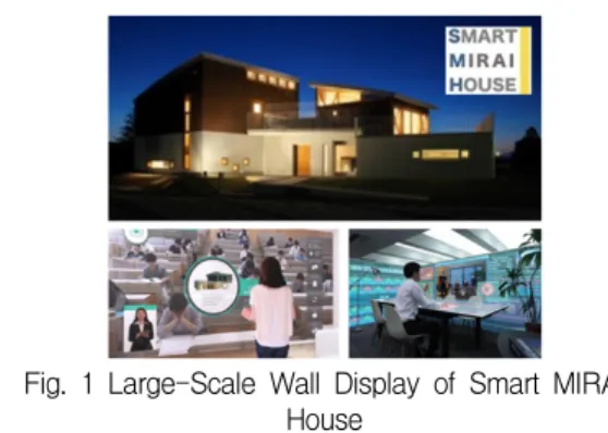
In particular, interest in flexible OLED displays is increasing [14-16]. The Smart MIRAI House of Yamagata University was built to demonstrate the living environment of the near future, as shown in Figure 1 [3, 17]. A large-scale wall display of the institution will be developed for video conferences, video telephony, and other communication media using organic material printing technology.
A gate driver is required to drive the OLED display. It is costly to use external drivers because many flexible printed circuits (FPCs) are involved.
Moreover, conventional chip on glass technology is not flexible. To reduce the manufacturing cost of the display panel and to simplify the module structure, a gate driver is integrated into the panel [18-21]. Thus, an integrated circuit (IC) bonding technology on the flexible panel is required.
Further, the problem associated with packing for the flexible panel should be solved. Therefore, it is necessary to fabricate an integrated gate driver using p-type OTFTs that can be manufactured by a panel process on a plastic substrate.
Fig. 1 Large-Scale Wall Display of Smart MIRAI House
In this paper, pseudo complementary metal oxide semiconductor (CMOS) logic gates are implemented using inkjet-printed OTFTs for a gate driver integrated in a flexible OLED display. The layout of the pseudo CMOS logic circuits based on the solution process rule of OTFTs was designed. The pseudo CMOS logics are fabricated using the same material and process as those of the display.
Moreover, the operation of the logic gates is confirmed by measurement.
The remainder of this paper is organized as follows. Section 2 describes the implementation of prototype flexible OLED displays with an OTFT backplane. OTFTs were manufactured to evaluate their transfer characteristics. The layout design and fabrication of pseudo CMOS logic circuits are discussed in Section 3. Section 4 reports the measurement results of the pseudo CMOS inverter and NAND gate. Finally, Section 5 concludes the paper.
Ⅱ. FLEXIBLE OLED DISPLAYS WITH AN OTFT BACKPLANE
We have successfully developed a 3.2-inch color flexible multiphoton emission OLED display driven by inkjet-printed OTFTs, as shown in Figure 2(a) [14-16, 21]. Figure 2(b) shows the structure of the OLED display using the color filter (CF) method.
The flexible display was constructed with a pixel circuit using OTFTs, white OLEDs, and a CF film (Dai Nippon Printing Co., Ltd.). The colorization of the display was achieved by the CF method that permits the transmission of white light from the OLED through a color filter that can switch between red, green, and blue. The CF was formed on a polyethylene naphthalate (PEN) film followed by patterning using photolithography. The careful lyophobic/lyophilic processing of the insulating material, bank structure, and organic semiconductor (OSC) ensured the high performance of the OLED display. OSCs were applied using the inkjet printing technique. The mobility of the OTFTs formed by coating the OSC solution using inkjet printing was approximately three times larger than that obtained using the solution-shearing method.
The flexible OLED display and drive circuits were connected via FPCs. Both images and videos were successfully displayed, even under bending.
(a) 3.2-inch Color (b) Structure of Display Fig. 2 Prototype of Flexible OLED Displays with the
OTFT Backplane
The gate driver was integrated into the panel to reduce the manufacturing cost of the display panel and to simplify the module structure for flexibility [18-21]. In addition, the display can be rolled, and
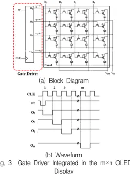
the characteristics of the flexible display can be exerted more strongly if the driving circuits can be formed with OTFTs. A gate driver (Figure 3(a)) using p-type OTFTs is required to drive the m×n OLED display and to be integrated on the plastic substrate. Figure 3(b) shows the waveform of the gate driver. Because the switching OTFTs of the panel are p-type devices, the output signal of the gate driver should be low to activate the horizontal line of the panel. The output signal of the gate driver is low and is sequentially shifted from O1 to Om to drive the m×n OLED display.
(a) Block Diagram
(b) Waveform
Fig. 3 Gate Driver Integrated in the m×n OLED Display
Ⅲ. STRUCTURE AND TRANSFER CHARACTERISTICS OF OTFT Figure 4 shows the structure of an inkjet-printed OTFT of bottom-gate/bottom-contact (BGBC) configuration [16]. A 50-nm-thick Al gate electrode layer was prepared by vacuum deposition and pattered by photolithography on glass or PEN film substrate. For gate dielectric layer 1,
cardo-polymer (GIP-2001/P2.5K; Nippon Steel &
Sumikin Chemical Co., Ltd.) was formed by the spin-coating solution process to obtain a 420-nm-thick film [22]. Gate dielectric layer 2 was formed by the chemical vapor deposition (CVD) of a 31-nm layer of Parylene (KISCO Ltd.). Au source/drain (S/D) electrodes, of 50-nm thickness, were prepared by vacuum deposition. The electrodes were patterned using conventional photolithography and wet etching. The banks to limit the spreading of the OSC solution were formed using a fluorine-based polymer (Teflon®
AF 1600, Dupont-Mitsui Fluorochemicals Company, Ltd.) by the spin-coating solution process and patterned by both wet and dry etching. Immediately before the OSCs had formed, the organic materials that had adhered to the S/D electrodes were removed using an ultraviolet (UV)-ozone cleaner;
thereafter, an electrode modification film was
formed by vapor treatment with
pentafluorobenzenethiol (PFBT). To create the OSCs, tetralin solvent containing 1 wt.%
DTBDT-C6 (Tosoh Corporation) and 0.25 wt.%
polystyrene (PS), which is a polymer-insulating material, was used [23-24]. The coating of the OSC solvent was achieved using an inkjet device (FUJIFILM Dimatix DMP-3000).
Fig. 4 Schematic of Inkjet-printed OTFT Structure
Fig. 5 Transfer Characteristics of OTFT Figure 5 shows the electrical transfer characteristics of an inkjet-printed OTFT measured in saturation at a drain-to-source voltage of –20 V. The OTFT was of depletion type. The channel width/length of the OTFT were 445 μm/5 μm. The field-effect mobility, on/off current ratio, and threshold voltage (Vth) were 0.73 cm2/(V·s), 1.9×10⁹, and 1.5 V, respectively.
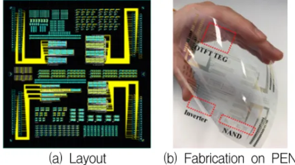
(a) Layout (b) Fabrication on PEN Fig. 6 Fabrication of pseudo CMOS logic circuits
Figure 6(a) shows the layout design of pseudo CMOS logic circuits based on the solution process rule of OTFTs for fabrication. The layout consisted of five layers: the gate, dielectric (including the contact hole layer), S/D, bank, and OSC layers.
The layout versus schematic (LVS) was verified.
Figure 6(b) shows the photograph of the fabricated pseudo CMOS logic circuits on flexible PEN for measurement.
Ⅳ. PSEUDO CMOS LOGICS USING OTFTS
It is necessary to fabricate the gate driver integrated in the flexible OLED display with backplane using an OTFT that can be manufactured by a panel process. Therefore, the gate driver should be designed as a pseudo CMOS logic, which is a logic gate using p-type OTFTs [9, 25-26].
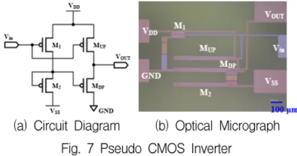
4.1 Pseudo CMOS Inverter
The pseudo CMOS inverter circuit consists of four p-type OTFT devices with different channel widths, as shown in Figure 7. Figure 7(a) shows the circuit diagram, and (b) shows the optical micrograph of the fabricated pseudo CMOS inverter circuit. The widths of M1 and M2 were 100 μm and 400 μm, respectively. The widths of M2, MUP, and MDP were the same.
(a) Circuit Diagram (b) Optical Micrograph Fig. 7 Pseudo CMOS Inverter
Figure 8(a) shows static transfer characteristics of the pseudo CMOS inverter at supply voltages (VDD) of 5, 10, 15, and 20 V, respectively, and tuning voltage VSS = –VDD. The inverter characteristics are typically obtained at the VDD of 5∼20 V by varying the input voltage (VIN) from 0 V to VDD. A value that is approximately the same as VDD is obtained when the output voltage (VOUT) is high (H), and almost 0 V is obtained when it is low (L). Hysteresis is observed in the characteristics of the OTFT. We found that hysteresis is affected by the OSC material and the processing method of the gate insulating film material. Figure 8(b) shows the gain characteristics
(the absolute value ΔVOUT/ΔVIN). The signal gain increases as VDD increases, and approximately 14 is obtained at 20 VDD.
(a) Static Characteristics (b) Signal Gain Fig. 8 Static Characteristics of Pseudo CMOS Inverter
Figure 9 shows the dynamic characteristics of the pseudo CMOS inverter. VDD is 20 V and VSS = -VDD. The VOUT performance was examined by changing the square wave with 50% duty ratio at 20 V to the input signal frequencies (fVin) of 10, 100, 500 Hz, and 1 kHz respectively, as the Vin. The measurement results show that the inverter can operate at an fVin of up to 1 kHz. Because the rising time and falling time of the VOUT are both approximately 0.5 ms, it becomes difficult to operate at an fVin of 1 kHz or beyond. To increase the speed of the pseudo CMOS inverter circuit, it is necessary to increase the output current of the OTFTs, and to decrease the parasitic capacitance.
The output current of the OTFTs can be increased by increasing the mobility of the OSCs, the ratio between the channel width and length, and the capacity of the gate insulating film.
Fig. 9 Dynamic Characteristics of Pseudo CMOS Inverter
4.2 Pseudo CMOS NAND
The pseudo CMOS NAND circuit consists of six p-type OTFT devices with different widths, as shown in Figure 10. Figure 10(a) shows the circuit diagram, and (b) shows the optical micrograph of the fabricated pseudo-CMOS NAND circuit. The width was set to 100 μm for both M1, M2, and 400 μm for M3 to M6. Figure 11 shows the static transfer characteristics of the NAND. This figure shows the result of setting the input voltage B (VB) to H (20 V) or L (0 V), and varying the input voltage A (VA) from 0 V to 20 V. During this measurement, VDD
was 20 V and VSS = -VDD. When VB was L, VOUT
was H and no change was observed. However, when VB was H, VOUT changed from H to L.
(a) Circuit Diagram (b) Optical Micrograph Fig. 10 Pseudo CMOS NAND
Fig. 11 Static Characteristics of Pseudo CMOS NAND
(a) fVB = 2 Hz (b) fVB = 20 Hz
(c) fVB = 200 Hz
Fig. 12 Dynamic Characteristics of Pseudo CMOS NAND
Figure 12 shows the dynamic characteristics of the pseudo-CMOS NAND. VDD is 20 V and VSS = -VDD. Figure 12(b) shows the VOUT when a square wave with VA with 50% duty ratio at fVA = 10 Hz, and a square wave with VB with 50% duty ratio at fVB = 20 Hz are input. As shown, VOUT is L (0 V) only when both VA and VB become H (20 V).
Figure 12(c) shows the VOUT when a square wave with a VA of 50% duty ratio at fVA = 100 Hz and a square wave with VB of 50% duty ratio at fVB = 200 Hz are input. In the case of fVB = 200 Hz, VOUT cannot be sufficiently decreased from H to L within 2.5 ms (half cycle of 200 Hz). To increase the operation speed of the pseudo CMOS NAND circuit, it is necessary to increase the output current of the OTFTs and to decrease the parasitic capacitance.
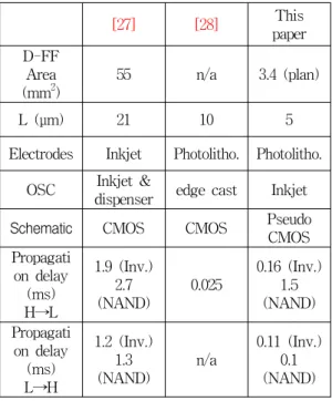
Table 1. Comparison of device specifications
[27] [28]
Thispaper D-FF
Area (mm2)
55 n/a 3.4 (plan)
L (μm) 21 10 5
Electrodes Inkjet Photolitho. Photolitho.
OSC Inkjet &
dispenser edge cast Inkjet
Schematic CMOS CMOS Pseudo
CMOS Propagati
on delay (ms) H→L
1.9 (Inv.) 2.7 (NAND)
0.025
0.16 (Inv.) 1.5 (NAND) Propagati
on delay (ms) L→H
1.2 (Inv.) 1.3 (NAND)
n/a
0.11 (Inv.) 0.1 (NAND)
Table 1 summarizes several device specifications of logic gate using OSC. The expected area of this paper is smaller than that of [27]. Furthermore, the
propagation delay time of this paper is shorter than that of [27]. Finally, pseudo CMOS inverter and NAND gates should be employed because inkjet-printed OTFTs and the same process as the display have to be used.
Ⅴ. CONCLUSION
For achieving a low manufacturing cost and simple module structure of a flexible OLED display panel with an active-matrix OTFT backplane, a gate driver was integrated into the panel using p-type OTFTs that were manufactured by a panel process. In this paper, a pseudo CMOS inverter and NAND gate were designed using inkjet-printed OTFTs. The layout of the pseudo CMOS logic circuits based on the solution process rule of OTFTs was designed. Furthermore, the pseudo CMOS logics were fabricated on flexible PEN. The operation of the logic gates was confirmed through measurement. In future work, we will fabricate shift registers and gate drivers using pseudo CMOS inverters and NAND gates and measure them. Moreover, we plan to integrate the flexible OLED display with the gate driver.
Acknowledgement
This paper is a revised and expanded version of a paper entitled “Design of Logic Gate Using Organic Transistor for Gate Driver of Flexible OLED Displays” presented at the 7th International Conference on Next Generation Computer and Information Technology, Hokkaido, Japan, August 23-25, 2018.
The authors would like to thank the Tosoh Corporation for providing the semiconductor material DTBDT-C6 and Nippon Steel &
Sumikin Chemical Co., Ltd. for providing the gate dielectric material GIP-2001/P2.5K.
The authors would like to thank Miho Abiko, and Kaori Watanabe for the process development and implementation of OTFT backplane for flexible OLED display.
References
[1] A. Yamamura, H. Matsui, M. Uno, N. Isahaya, Y. Tanaka, M. Kudo, M. Ito, C. Mitsui, T.
Okamoto, and J. Takeya, “Painting integrated complementary logic circuits for signal-crystal organic transistors : A demonstration of a digital wireless communication sensing tag,”
Advanced Electronic Materials, vol. 3, no. 7,
2017, Art. no. 1600456.[2] R. Shiwaku, H. Matsui, K. Nagamine, M.
Uematsu, T. Mano, Y. Maruyama, A.
Nomura, K. Tsuchiya, K. Hayasaka, Y.
Takeda, T. Fukuda, D. Kumaki, and S.
Tokito, “A printed organic circuit system for wearable amperometric electrochemical sensors,” Scientific Reports, vol. 8, 2018, Art.
no. 6368.
[3] S. Cho and M. Yokoyama, “Integrated design of low-power adiabatic dynamic CMOS logic using 0.18μm standard CMOS model for circadian rhythm OLED illumination system,”
Int. J. of Control and Automation, vol. 10, no.
11, 2017, pp. 51-60.
[4] C. Dimitrakopoulos and P. Malenfant, “Organic thin film transistors for large area electronics,” Advanced Materials, vol. 14, no. 2, 2002, pp. 99-117.
[5] T. Someya, Y. Kato, S. Iba, Y. Noguchi, T.
Sekitani, H. Kawaguchi, and T. Sakurai,
“Integration of organic FETs with organic photodiodes for a large area, flexible, and lightweight sheet image scanners,” IEEE
Trans. on Electron Devices, vol. 52, no. 11,
2005, pp. 2502-2511.[6] E. Cantatore, T. Geuns, G. Gelinck, E.
Veenendaal, A. Gruijthuijsen, L.
Schrijnemakers, S. Drews, and D. Leeuw, “A 13.56-MHz RFID system based on organic transponders,” IEEE J. of Solid-State Circuits, vol. 42, no. 1, 2007, pp. 84-92.
[7] T. Chiba, Y. Pu, and J. Kido, “Organic light-emitting devices with tandem structure,”
Topics in Current Chemistry, vol. 374, no. 3,
2016, pp. 1-17.[8] D. Yang, H. Sasabe, Y. Jiao, T. Zhuang, Y.
Huang, X. Pu, T. Sano, Z. Lu, and J. Kido,
“An effective π-extended squaraines for
solution processed organic solar cells with high efficiency,” J. of Materials Chemistry A, vol. 4, no. 48, 2016, pp. 18931-18941.
[9] T. Huang, K. Fukuda, C. Lo, Y. Yeh, T.
Sekitani, T. Someya, and K. Cheng,
“Pseudo-CMOS: A design style for low-cost and robust flexible electronics,” IEEE Trans.
on Electron Devices, vol. 58, no. 1, 2011, pp.
141-150.
[10] K. Fukuda, Y. Takeda, Y. Yoshimura, R.
Shiwaku, L. T. Tran, T. Sekine, M. Mizukami, D. Kumaki, and S. Tokito, “Fully-printed high-performance organic thin-film transistors and circuitry on one-micron-thick polymer films,” Nature Communications, vol. 5, 2014, Art. no. 4147.
[11] T. Sekitani, M. Takamiya, Y. Noguchi, S.
Nakano, Y. Kato, T. Sakurai, and T. Someya,
“A large-area wireless power-transmission sheet using printed organic transistors and plastic MEMS switches,” Nature Materials, vol.
6, 2007, pp. 413-417.
[12] A. Vornbrock, D. Sung, H. Kang, R.
Kitsomboonloha, and V. Subramaian, “Fully gravure and ink-jet printed high speed pBTTT organic thin film transistors,” Organic
Electronics, vol. 11, no. 12, 2010, pp.
2037-2044.
[13] K. Fukuda, Y. Yoshimura, T. Okamoto, Y.
Takeda, D. Kumaki, Y. Katayama, and S.
Tokito, “Reverse-offset printing optimized for scalable organic thin-film transistors wit submicrometer channel lengths,” Advanced
Electronic Materials, vol. 1, no. 8, 2015, Art.
no. 1500145.
[14] M. Mizukami, S. Oku, S. Cho, M. Tatetsu, M.
Abiko, M. Mamada, T. Sakanoue, Y. Suzuri, J.
Kido, and S. Tokito, “A solution-processed organic thin-film transistor backplane for flexible multiphoton emission organic light-emitting diode displays,” IEEE Electron
Device Letters, vol. 36, no. 8, 2015, pp.
841-843.
[15] Y. Pu, T. Chiba, K. Ideta, S. Takahashi, N.
Aizawa, T. Hikichi, and J. Kido, “Fabrication of organic light-emitting devices comprising stacked light-emitting units by solution-based processes,” Advanced Materials, vol. 27, no. 8,
2015, pp. 1327-1332.
[16] M. Mizukami, S. Cho, K. Watanabe, M.
Abiko, Y. Suzuri, S. Tokito, and J. Kido,
“Flexible organic light-emitting diode displays driven by inkjet printed high mobility organic thin film transistors,” IEEE Electron Device
Letters, vol. 39, no. 1, 2018, pp. 39-42.
[17] S. Cho, S. Yeo, S. Kim, and M. Yokoyama,
“Optimization of control block of 3-bit PWM using adiabatic dynamic CMOS logic for OLED illumination system based on internet of things service,” Int. J. of Smart Home, vol.
10, no. 9, 2016, pp. 317-328.
[18] N. Noda, N. Kobayashi, M. Katsuhara, A.
Yumoto, S. Ushikura, R. Yasuda, N. Hirai, G.
Yukawa, I. Yagi, K. Nomoto, and T. Urabe,
"An OTFT-driven rollable OLED display," J. of
the Society for Information Display, vol. 19, no.
4, 2011, pp. 316-322.
[19] W. Wu, L. Zhang, Z. Xu, L. Zhou, H. Tao, J.
Zou, M. Xu, L. Wang, and J. Peng, “A high-reliability gate driver integrated in flexible AMOLED display by IZO TFTs,”
IEEE Trans. on Electron Devices, vol. 64, no. 5,
2017, pp. 1991-1996.[20] L. Dulau, S. Pontarollo, A. Boimond, J.
Garnier, N. Giraudo, and O. Terrasse, “A new gate driver integrated circuit for IGBT devices with advanced protections,” IEEE
Trans. on Power Electronics, vol. 21, no. 1,
2006, pp. 38-44.[21] S. Cho and M. Mizukami, “Design of shift register using organic thin film transistor for gate driver of flexible organic light-emitting diode displays,” Int. J. of Advanced Science and
Technology, vol. 111, 2018, pp. 147-156.
[22] K. Mizuuchi, H. Kawasato, M. Takeuchi, S.
Inaba, and T. Teramoto, “High-resolution cardo polymer dielectric ‘VPA-series’,” In
Proc. 52nd Electronic Components and Technology Conference, San Diego, USA, May 2002, pp.
28-31.
[23] Y. Kimura, T. Nagase, A. Hamaguchi, Y.
Ikeda, T. Shiro, K. Takimiya, and H. Naito,
“Soluble organic semiconductor precursor with specific phase separation for high-performance printed organic transistors,” Advanced Materials, vol. 27, no. 4, 2015, pp. 727-732.
[24] R. Shiwaku, Y. Takeda, T. Fukuda, K.
Fukuda, H. Matsui, D. Kumaki, and S.
Tokito, “Printed 2 V-operating organic
inverter arrays employing a
small-molecule/polymer blend,”
Scientific Reports, vol. 6, 2016, Art. no. 34723.
[25] Y. Takeda, Y. Yoshimura, Y. Kobayashi, D.
Kumaki, K. Fukuda, and S. Tokito,
“Integrated circuits using fully solution-processed organic TFT devices with printed silver electrodes,” Organic Electronics, vol. 14, no. 12, 2013, pp. 3362-3370.
[26] Q. Zhao, W. Sun, J. Zhao, L. Feng, X. Xu, W.
Liu, X. Guo, Y. Liu, and H. Yang, “Noise Margin, Delay, and Power Model for Pseudo-CMOS TFT Logic Circuits,” IEEE
Trans. on Electron Devices, vol. 64, no. 6, 2017,
pp. 2635-2642.[27] K. Hayasaka, H. Matsui, Y. Takeda, R.
Shiwaku, Y. Tanaka, T. Shiba, D. Kumaki, and S. Tokito, “Compact organic complementary D-type flip-flop circuits fabricated with inkjet printing,” Advanced
Electronic Materials, vol. 3, no. 9, 2017, Art.
no. 1700208.
[28] M. Uno, N. Isahaya, B. Cha, M. Omori, A.
Yamamura, H. Matsui, M. Kudo, Y. Tanaka, Y. Kanaoka, M. Ito, and J. Takeya,
“High-yield, highly uniform solution‐
processed organic transistors integrated into flexible organic circuits,” Advanced Electronic
Materials, vol. 3, no. 1, 2017, Art. no. 1600410.
저자소개
조승일(Seung-Il Cho) 2013년 일본 Yamagata Univ. 이 공학연구과(공학박사)
2013년 ∼현재 일본 Yamagata Univ. Innovation Center for Organic Electronics Assistant Professor
※ 관심분야 : Organic TFT 집적회로 설계, Adiabatic log circuit, 아날로그 디지털 mixed 회로 설계
Makoto Mizukami 2018년 일본 Yamagata Univ. 이 공학연구과(공학박사)
2011년 ∼현재 일본 Yamagata Univ. Innovation Center for Organic Electronics Associate Professor
※ 관심분야 : Organic TFT, organic light emitting diode (OLED) flexible displays