반도체디스플레이기술학회지 제18권 제3호(2019년 9월)
Journal of the Semiconductor & Display Technology, Vol. 18, No. 3. September 2019.
Needle 코팅을 이용한 미세 PEDOT:PSS 스트라이프 제작
이진영*· 박종운**†
*한국기술교육대학교 창의융합공학협동과정,
**†한국기술교육대학교 전기·전자·통신공학부
Fabrication of Fine PEDOT:PSS Stripes Using Needle Coating
Jinyoung Lee
*and Jongwoon Park
**†*Interdisciplinary Program in Creative Engineering,
**†School of Electrical & Communication Engineering, Korea University of Technology and Education
ABSTRACT
We have investigated the feasibility of fabricating fine stripes using needle coating for potential applications in solution-processed organic light-emitting diodes (OLEDs). To this end, we have employed an aqueous poly(3,4- ethylenedioxythiophene):poly(4-styrenesulfonate) (PEDOT:PSS) solution that has been widely used as a hole injection layer (HIL) of OLEDs and performed needle coatings by varying the process parameters such as the coating gap and coating speed. As expected, the stripe width is reduced with increasing coating speed. However, the central thickness of the stripe is rather increased as the coating speed increases, which is different from other coating processes such as slot-die and blade coatings. It is due to the fact that the meniscus formed between the needle tip and the substrate varies depending sensitively on the coating speed. It is also found that the stripe width and thickness are reduced with increasing coating gap. To demonstrate its applicability to OLEDs, we have fabricated a red OLED stripe and obtained light emission with the width of about 90 µm.
Key Words : Needle coating, Fine stripe, PEDOT:PSS, Solution process, OLED
1. 서 론1
용액 공정(solution process)은 저비용, 고효율, 높은 확장성 등의 장점으로 인해 미세 박막 형성을 요하는 센서, 메탈 전극, 태양전지, 디스플레이 등 다양한 분야에서 적용되 고 있다[1]. 용액 공정은 미세 패턴 형성에 적합한 프린팅 (printing) 공정과 대면적 박막 형성이 용이한 코팅(coating) 공정으로 나뉜다[2]. 잉크젯, 노즐, 그라비어, 오프셋과 같 은 프린팅 기술은 수십 µm 이하의 미세 패턴 형성이 용 이하지만 박막 표면 거칠기 및 두께 균일도가 상대적으 로 좋지 않으며 다양한 점도의 잉크를 사용할 수 없는 문
†
E-mail: [email protected]
제를 가지고 있다. 이에 반해 스핀, 블레이드, 슬롯과 같 은 코팅 기술은 대면적 고균일 박막 형성이 용이한 반면 해상도가 낮아 미세 stripe 패턴 형성이 어렵다. 하지만 우 리는 이전 연구에서 슬롯 다이 코팅(slot-die coating)을 이용 하여 89 µm 폭을 갖는poly(3,4-ethylenedioxythiophene):poly(4- styrenesulfonate) (PEDOT:PSS) stripe를 제작할 수 있음을 보 였다[3].
본 연구에서는 슬롯 다이 코팅 외에도 니들 코팅(needle coating)을 이용하여 미세 stripe 박막 형성이 가능한지 연구 하였다. Needle 코팅 기술은 미세한 시린지(syringe) needle을 사용하여 미세 패턴을 형성하는 기술로 비용이 저렴하고 공정이 간단한 장점을 가지고 있다. 이러한 needle 코팅을 이용하여 은나노와이어(AgNWs)를 기반으로 하는 용량성
Needle 코팅을 이용한 미세 PEDOT:PSS 스트라이프 제작 101
센서(capacitive sensor)가 제작되었고[4] 하이브리드 폴리머 를 사용한 나노테르밋(nanothermite) 스틱을 제작하는 연구 [5], 전자 회전 PVP 나노파이버(nanofiber)를 제작하는 연구 [6] 등이 진행되었다. 최근까지 needle 코팅을 이용하여 제 작된 미세 패턴의 폭은 500µm 이상으로 매우 넓으며 적 용된 분야 또한 전극, 센서 등으로 협소하다. Needle 코팅 을 디스플레이나 반도체 분야에 적용하기 위해서는 보다 좁은 폭을 갖는 스트라이프 박막을 형성할 필요가 있다.
이를 위해서 코팅 시 needle에 형성되는 용액 분포를 정밀 하게 분석하였으며 코팅 갭, 코팅 속도 등 공정 변수 (process parameters)에 따른 박막 특성 변화를 측정/분석 하였다.
2. 실험 방법
(a)
(b)
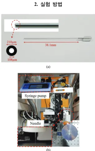
Fig. 1. (a) Image of a needle nozzle and (b) roll-to-roll
coating system used for experiments.실험을 위해 210µm 외경과 108µm 내경을 갖는 needle (Hamilton 사 구매)을 사용하였다 (Fig. 1(a)). 코팅은 롤투롤 장비를 이용하였으며 Fig. 1(b)와 같이 needle을 거치대에
고정한 후 polyethylene terephthalate (PET) 롤 기판 필름과 수 직이 되도록 설치하였으며 시린지 펌프(11 Elite I/W single, Harvard Apparatus)와 연결하였다. 코팅 용액으로 OLED 정 공 주입층(hole injection layer, HIL)용으로 널리 쓰이는 수계 PEDOT:PSS (Clevios AI 4083)을 사용하였으며 젖음성을 높여 용액이 필름 위에 코팅이 잘되도록 하기 위해 불소계 계 면활성제를 0.1wt% 첨가하였다. 최소 폭을 갖는 stripe을 제작하기 위하여 코팅 속도(coating speed), 기판과 needle 간 의 코팅 갭(gap) 등의 변수들을 조절하면서 코팅을 진행하 였다. 코팅 도중 needle tip 과 기판 사이에 형성되는 메니 스커스(meniscus) 및 용액 분포를 area scan camera (acA1300- 30gm, BASLER)를 사용하여 측정하였다. 3D laser microscope (VK-8700, KEYENCE)를 사용하여 코팅된 stripe의 프로파일 을 측정하였다.
3. 결과 및 고찰
먼저 needle 코팅의 여러 변수들을 조절하여 최소 코팅 폭을 형성할 수 있는 최적의 조건을 조사하였다. 이를 위 해 코팅 갭은 20µm, 유량은 0.001ml/min로 설정한 후 코팅 속도를 변경하며 stripe 폭 및 두께 변화를 측정하였으며 그 결과를 Figs. 2-4 와 Table 1에 정리하였다. Figs. 2-3에서 보 듯이, 토출량이 일정한 상태에서 코팅 속도가 증가하면 코팅된 stripe의 폭(width, W)은 줄어들면서 중심 두께 (thickness, T)는 증가함을 알 수 있다. 이는 needle tip과 기판 사이에서 형성되는 meniscus의 폭이 코팅 속도가 증가하 면서 감소하기 때문이다(Fig. 4). 즉, 코팅 속도가 감소하면 토출된 용액이 많아 needle tip 외경으로 용액이 퍼지기 때 문에 Fig. 4(a)와 같은 넓은 분포를 갖는다. 하지만 코팅 속 도가 증가하면 Fig. 4(b)와 같이 용액이 팁 내경으로 몰리 면서 코팅 폭이 좁아지게 된다. 이때 토출량이 일정한 상 태에서 메니스커스 폭이 줄어들기 때문에 중심두께는 증 가하게 된다. 코팅속도 30 mm/s에서 최소 stripe 폭을 얻을 수 있지만 stripe 폭 편차(31.5%)가 크고 중심두께 편차가 너무 크게 나타났다. 이는 코팅 속도가 빨라지면 메니스 커스의 흔들림이 커지기 때문이다. 따라서 최소 폭을 가 지면서 폭 균일도가 우수한 stripe 박막을 얻을 수 있는 최 적(고) 코팅 속도는 27 mm/s이며 이 조건에서 폭 106 µm, 두께 145nm를 갖는 stripe를 얻었다. 한편, 코팅 속도가 10mm/s이하로 너무 낮으면 stripe 두께 균일도가 급격히 나 빠진다. 이는 Fig. 4(a)에서 보듯이 코팅 속도가 낮으면 needle tip 외경으로까지 용액이 분포되고 모세관 현상에 의 해 용액이 needle을 타고 상승하다가 일정 이상 용액이 쌓이 면 떨어지기를 반복하면서 두께 편차가 커지기 때문이다.
이진영 · 박종운 102
(a)
(b)
(c)
Fig. 2. Measured optical image of the PEDOT:PSS stripes
coated at (a) 20mm/s, (b) 27mm/s, and (c) 30mm/s when the flow rate is 0.001ml/min and coating gap is 20 µm.Table 1. Summary of measured thickness (T) and width (W)
of PEDOT:PSS stripes coated at different coating speedsSpeed (mm/s) W (µm) T (nm)
20 130-136 117-126
27 104-109 139-151
30 72-99 -
다음으로 코팅 갭에 따른 박막 특성 변화를 조사하기 위하여 최적(고) 코팅속도 27 mm/s에서 코팅 갭을 20µm, 50µm, 70µm로 변화시키며 코팅을 진행하였다. Fig. 5에서 보듯이 코팅 갭이 증가하면 stripe 폭 및 두께가 감소함을 알 수 있다. 즉, strip 폭은 106µm (코팅 갭=20µm)에서 103µm (코팅 갭=50µm), 91 µm(코팅 갭=70µm)으로 감소하였으며
Fig. 3. Measured profiles of the PEDOT:PSS stripes coated
at different coating speeds when the flow rate is 0.001ml/min.(a)
(b)
Fig. 4. Schematic view of solution distribution during
needle coating when the coating speed is (a) low and (b) high.
stripe 두께도 145nm (코팅 갭=20µm)에서 114nm(코팅 갭
=50µm), 98 nm(코팅 갭=70µm)로 감소하였다. 이는 Fig. 6에 보여지듯이, 코팅 갭이 증가하면서 needle tip과 기판 사이
Needle 코팅을 이용한 미세 PEDOT:PSS 스트라이프 제작 103
에 형성되는 meniscus (또는 용액분포)가 좁아지기 때문이 다. 코팅 갭이 90µm이상으로 매우 높을 경우에는 기판과 needle tip 간의 간격이 너무 멀어서 meniscus가 needle tip과 기판 사이에서 bridge 역할을 할 수 없어 stripe이 끊기거나 stripe이 형성되더라도 균일한 박막을 얻을 수 없다.
Fig. 5. Measured stripe profiles for different coating gaps at
the coating speed of 27mm/s.(a)
(b)
(c)
Fig. 6. Measured flow distribution near the needle tip at
27mm/s when the coating gap is (a) 20µm, (b) 50µm and (c) 70µm.
Fig. 7. A layer structure of phosphorescent red OLED device.
마지막으로 needle 코팅을 습식기반 OLED 디스플레이 공정에 적용할 수 있는지 알아보기 위하여 전도성 PEDOT:PSS (PH1000, Clevios)를 이용하여 미세 OLED stripe를 제작하였다 (Fig. 7). 롤 필름 위에 needle 코팅을 이용하여 토출량 0.001ml/min, 코팅 갭 70µm, 코팅 속도 27 mm/s에서 미세 PEDOT:PSS를 stripe 코팅 한 뒤 열 증착기(thermal evaporator)를 사용하여 적색 인광 OLED 소자를 제작하였 다. 정공 주입층으로 KHI-001 (Duksan Neolux)을 15nm 증착 하였고 정공 수송층(HTL, hole transport layer)으로 N,N'-Bis(3- methylphenyl)-N,N' -bis(phenyl)-benzidine (TPD)를 40nm 증착하 였다. 발광층(EML, emission layer)으로는 4,4'-bis(N-carbazolyl)- 1,1'-biphenyl (CBP)에 Bis[2-(3,5-dimethylphenyl)-4-methyl-quinoline]
(acetylacetonate) iridium(III) Ir(mphmq)2acac을 8wt% 도핑하여 15nm 두께로 증착하였다. 정공 차단층(HBL, hole blocking layer)으로는 4,7-diphenyl-1,10-phenanthroline (Bphen)을 10nm 증 착하였으며, 전자 수송층(ETL, electron transport layer)으로는 tri-(8-hydroxyqunoline) aluminum (Alq3)를 30nm 증착하였다. 전 자 주입층(EIL, electron injection layer)으로는 lithium fluoride (LiF) 를 사용하여 1nm 두께로 증착한 후 음극으로 aluminum (Al) 을 100nm 두께로 증착하였다. Fig. 8은 4cm 길이를 갖는 적 색 인광 OLED stripe의 발광 이미지를 광학현미경과 카메 라로 측정한 결과이다. Fig. 8에서 보이듯, OLED stripe의 발
Fig. 8. Image of light emission from 4-cm-long red OLED
stripe at the bias current of 150μA.이진영 · 박종운 104
광 폭은 대략 90µm으로 PEDOT:PSS stripe 폭과 거의 같으 며 경계 구분이 뚜렷하게 보였다. 또한 전 영역에서 균일 하게 발광하는 것을 확인하였다. 하지만 봉지(encapsulation) 공정을 거치지 않았기 때문에 소수의 dark spot이 나타났다.
4. 결 론
본 연구에서는 needle 코팅을 이용하여 OLED화소 형성 에 적용할 수 있는 미세 PEDOT:PSS stripe 제조 가능성을 연 구하였다. 외경 210µm, 내경108µm를 갖는 needle을 이용하 여 토출량 0.001ml/min, 코팅 갭 70µm, 코팅 속도 27 mm/s에 서 폭 91 µm와 두께 98nm를 갖는 PEDOT:PSS stripe를 제조하 였다. 또한 이를 이용하여 비슷한 폭(발광)을 갖는 인광 적 색 OLED stripe를 제작하는데 성공하였다. 본 연구에서 다 른 코팅(슬롯, 블레이드) 공정과 달리, needle 코팅은 코팅 속 도가 증가할수록 오히려 중심두께가 증가하는 현상을 발 견하였다. 이는 needle tip과 기판 사이에 형성되는 meniscus 가 코팅속도가 증가하면서 변화(좁아짐)하기 때문이다.
감사의 글
This research was supported by Basic Science Research Program through the National Research Foundation of Korea (NRF) (NRF- 2018R1D1A1B07042248) funded by the Ministry of Education.
참고문헌
1. Ye, D., Ding, Y., Duan, Y., Su, J., Yin, Z, and Huang, Y.,
“Large-Scale Direct-Writing of Aligned Nanofibers for Flexible Electronics,” Small, Vol. 14, p. 1703521, 2018.
2. Kim, B. et al., “High-Resolution Patterns of Quantum Dots Formed by Electrohydrodynamic Jet Printing for Light-Emitting Diodes”, Nano Lett., Vol. 15, pp. 969- 973, 2015.
3. Yoo, S., Lee, J., and Park, J., “Simulation of Capillary Flow Along a Slot-die Head for Stripe Coatings,” J. of
The Korean Society of Semiconductor & Display Technology, Vol. 18, pp. 51-52, 2019.
4. Li, R., Hu, A., Zhang, T., and Oakes, K., “Direct Writing on Paper of Foldable Capacitive Touch Pads with Silver Nanowire Inks,” ACS Appl. Mater. Interfaces, Vol. 6, pp.
21721-21729, 2014.
5. Wang, H. et al., “Direct Writing of a 90 wt% Particle Loading Nanothermite,” Adv. Mater., Vol. 31, p.
1806575, 2019.
6. Matatagui, D. et al., “Real-Time Characterization of Electrospun PVP Nanofibers as Sensitive Layer of a Surface Acoustic Wave Device for Gas Detection,” J.
Nanostruct., Vol. 21, pp. 1-8, 2014.
접수일: 2019년 9월 10일, 심사일: 2019년 9월 19일, 게재확정일: 2019년 9월 23일