논문 2011-48SD-3-1
N-Channel 산화물 TFT 기반의 저소비전력 논리 게이트 회로
( Low Power Digital Logic Gate Circuits Based on N-Channel Oxide TFTs )
임 도*, 박 기 찬**, 오 환 술****
( Tao Ren, KeeChan Park, and HwanSool Oh )
요 약
N-channel 산화물 박막 트랜지스터(Thin Film Transistor, 이하 TFT)만을 이용한 저소비전력 inverter, NAND, NOR의 논 리 게이트 회로를 제안한다. 제안된 회로는 asymmetric feed-through와 bootstrapping을 이용해서 pull-up, pull-down 스위치 가 동시에 켜지지 않도록 설계하였다. 그 결과로 출력신호 전압 범위가 입력신호 전압과 동일하고 정전류가 흐르지 않는다. 인 버터는 5 개의 TFT와 2 개의 capacitor로, NAND 및 NOR 게이트는 각각 10 개의 TFT와 4 개의 capacitor로 구성된다. 산화 물 TFT 모델을 사용하여 SPICE 시뮬레이션을 수행하여 제안된 회로의 동작을 성공적으로 검증하였다.
Abstract
Low-power logic gates, i.e. inverter, NAND, and NOR, are proposed employing only n-channel oxide thin film transistors (TFTs). The proposed circuits were designed to prevent the pull-up and pull-down switches from being turned on simultaneously by using asymmetric feed-through and bootstrapping, thereby exhibited same output voltage swing as the input signal and no static current. The inverter is composed of 5 TFTs and 2 capacitors. The NAND and the NOR gates consist of 10 TFTs and 4 capacitors respectively. The operations of the logic gates were confirmed successfully by SPICE simulation using oxide TFT model.
Keywords : n-channel oxide TFT, logic gate, low power, asymmetric feed-through, bootstrapping
Ⅰ. Introduction
The metal oxide, e.g. In-Ga-Zn-O, thin film transistor (TFT) allows for high-frame-rate driving of high-resolution active-matrix liquid-crystal display (AMLCD) owing to high mobility (>10cm2/Vs) compared with the prevailing amorphous silicon
* 정회원, ** 정회원-교신저자, *** 평생회원, 건국대학교 전자공학부
(Department of Electronic Engineering, Konkuk University)
※ 이 논문은 2010 년도 정부(교육과학기술부)의 재원 으로 한국연구재단의 기초연구사업 지원을 받아 수 행된 것임(2010-0016423).
접수일자: 2011년1월13일, 수정완료일: 2011년2월22일
(a-Si) TFT[1]. In addition it exhibits better uniformity and lower fabrication cost than the polycrystalline silicon (poly-Si) TFT[2-4]. With its excellent switching property and high current driving capability, the oxide TFT is the most promising device for next-generation active-matrix flat-panel display (AMFPD).
However the oxide TFT operates only as an n-channel field effect transistor (FET). Therefore it is troublesome to integrate digital circuits using the oxide TFTs. Although digital logic gates such as inverter, can be constructed using only n-channel FETs or p-channel FETs, they are much inferior to
effect to drive the n-channel pull-up TFTs. A similar technique was previously proposed by S. H. Jung et al. for a p-channel TFT inverter in which the pull-up TFTs and the pull-down TFTs are turned on and off completely according to the input signals, which eliminates the static current flow from the supply voltage sources (VDD)[8]. We expands this scheme to other logic circuits such as NAND and NOR gates based on n-channel oxide TFTs.
Ⅱ. Characteristics of Oxide TFTs
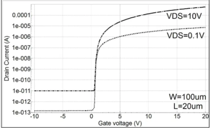
Figure 1 shows the transfer characteristics of the oxide TFT model for SPICE simulation. We used the RPI a-Si TFT model (level=35) in the SmartSpiceTM. The channel width (W) and the length (L) of the TFT are 100μm and 20μm, respectively. Threshold voltage (VT) is 2V and the field effect mobility is 10cm2/Vs. On/off current ratio is approximately 108 and IOFF is as low as 10-13A/μm. In this paper, all the simulation results are obtained using this TFT model.
그림 1. 산화물 TFT의 전달특성
Fig. 1. Transfer characteristics of oxide TFTs.
as the input voltage range. In the subsequent explanation, the input voltage is 0V-20V and the resultant output voltage also becomes 0V-20V.
When the input signal is 20V, M3, M4 and M5 are turned on, which makes nodes A and B pulled down to VSS(0V). Accordingly M1 and M2 are turned off.
Then the output voltage is equal to VSS without any current flow from VDD1 or from VDD2 to VSS.
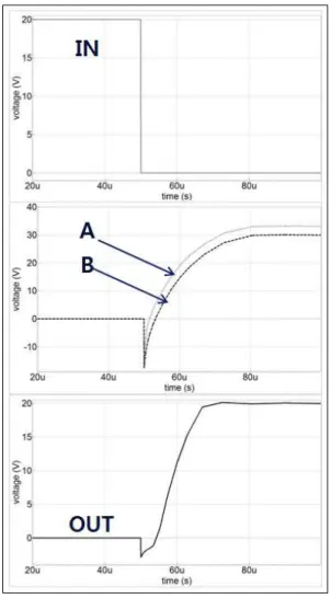
When the input signal falls off from 20V to 0V, M3, M4, and M5 are turned off. At the same time, the voltages at nodes A and B also go down abruptly by capacitive coupling as shown in Fig. 3. However the voltage drop at node B is larger than that at node A because the capacitance of CC is larger than the gate capacitance of M3. This asymmetric feed-through turns on M1. Accordingly the voltage at node B is pulled-up by charge flow from VDD2 through M1. During this period, the voltage at floating node A also rises by capacitive coupling
그림 2. N-channel oxide TFT를 이용한 인버터 회로 Fig. 2. Inverter circuit using only n-channel oxide TFTs.
그림 3. 모의실험 파형도: 입력, 출력, 노드 A 및 노드 B
Fig. 3. Simulated waveform: Input, output, node A, and node B.
through CH and finally it may exceed VDD2 as shown in Fig. 3. This bootstrapping effect transfers whole VDD2 to the node B without VT-drop.
Therefore M2 is turned on with gate voltage of VDD2 that is higher than VDD1 and the output voltage is exactly equal to VDD1. The capacitor CH
maintains the voltage difference between the nodes A and B during this output-high period. In summary, M2 pulls up the output with the aids of M1, M3 and M4. Firstly, M3, M4 and CC induces asymmetric feed-through. Next, M1 raises the voltages at the nodes A and B by bootstrapping. It should be noted that no current flows at all when the steady state is reached because M3, M4, and M5 are turned off.
Figure 4 shows that the output of the inverter is
그림 4. 인버터 회로의 SPICE 모의실험 결과 Fig. 4. SPICE simulation results of inverter circuit.
exactly the inverse of the input signal. The rise time is larger than the fall time because the gate-to-source voltage of M1 - voltage difference of node A and B in Fig. 3 - is small while the output changes from low to high. Fig. 4 confirms that the current from VDD1 or VDD2 flows only when the signals change. There is no static current while the signals retain steady state like the CMOS inverter.
So the power consumption of the inverter circuit is, in principle, comparable to that of the CMOS inverter.
The channel widths of the TFTs M1-M5 are 200, 200, 80, 40, and 40μm, respectively. The channel lengths are 20μm for all TFTs.
Ⅳ. NAND Gate
The inverter can be incorporated into other digital logic gates such as NAND gate. The basic operation of an ideal NAND gate is shown in Fig. 5. When IN1 or IN2 is low, the output is high. The output is low only when both inputs are high. In other words, the output is high in most cases and it is low if and only if both IN1 and IN2 are high. So two switches controlled by IN1 and by IN2 respectively should be connected in series in the pull-down part and in parallel in the pull-up part. Fig. 6 shows that two pull-down TFTs M5 and M10 are connected in series and that two pull-up parts identical to that of the inverter are connected in parallel.
The NAND gate circuit operates as follows. When
그림 6. N-channel oxide TFT를 이용한 NAND 게이트 Fig. 6. NAND gate using only n-channel oxide TFTs.
IN1 and IN2 are high (T1 in Fig. 5), TFTs M3-M5 and M8-M10 are turned on, which makes M1, M2, M6, and M7 turned off. Accordingly the output drops to VSS. When IN1 is high and IN2 becomes low (T2 in Fig. 5), M3-M5 are still turned on, keeping M1 and M2 in the left half turned off. However the output is not connected to VSS because M10 is turned off in the pull-down part. In the right half, M8-M10 are turned off, so M6 and M7 are turned on by asymmetric feed-through and bootstrapping. This makes the output connected to VDD1 through M7. In the opposite case when IN1 is low and IN2 is high (T3 in Fig. 5), the output is connected to VDD1 through M2. When both IN1 and IN2 are low (T4 in Fig. 5), the pull-up TFTs M1, M2, M6, and M7, are turned on, whereas the TFTs M3-M5 and M8-M10 that are connected to VSS are turned off. Therefore the output is connected to VDD1 through M2 and M7 in this period.
그림 7. NAND 게이트의 SPICE 모의실험 결과 Fig. 7. SPICE simulation results of NAND gate.
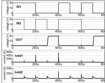
Fig. 7 shows that the input and output waveforms of the NAND gate are same as the timing diagram of an ideal NAND gate shown in Fig. 5. It should be noted again that the current from VDD1 or VDD2 is observed only when the signals change. There is no static current as long as the signals retain steady state. The sizes of the TFTs used in the simulation of the NAND gate are identical to those of the inverter.
Ⅴ. NOR Gate
A NOR gate also can be constructed by employing the inverter. The basic operation of an ideal NOR gate is shown in Fig. 8. When IN1 or IN2 is high, the output is low. The output is high only when both inputs are low. In other words, the output is low in most cases and it is high if and only if both IN1 and IN2 are low. Therefore two pull-up switches that are controlled inversely by IN1 and IN2 respectively are connected in series as shown in Fig. 9 - M2 and M7.
Although two pull-down TFTs M5 and M10 are not connected directly in parallel, M5 pulls down the output through M7 when IN1 is high and IN2 is low.
The NOR gate circuit operates as follows. When IN1 and IN2 are high (T1 in Fig. 8), TFTs M3-M5 and M8-M10 are turned on, which makes M1, M2, M6, and M7 turned off. Accordingly the output is
그림 8. NOR 게이트의 타이밍도 Fig. 8. Timing diagram of NOR gate.
그림 9. N-channel oxide TFT를 이용한 NOR 게이트 Fig. 9. NOR gate using only n-channel oxide TFTs.
connected to VSS through the pull-down TFT M10 and the output drops to VSS. When IN1 is high and IN2 becomes low (T2 in Fig. 8), TFTs M3-M5 are still turned on keeping M1 and M2 in the upper half turned off. In the lower half, M8-M10 are turned off, so M6 and M7 are turned on. At this time, the output is connected to VSS through M5 and M7. In the opposite case when IN1 is low and IN2 is high (T3 in Fig. 8), the output is connected to VSS through M10. Finally, When both IN1 and IN2 are low (T4 in Fig. 8), the pull-up TFTs M1, M2, M6, and M7 are turned on, whereas the TFTs M3-M5 and M8-M9 that are connected to VSS are turned off. Therefore the output is connected to VDD1
그림 10. NOR 게이트의 SPICE 모의실험 결과 Fig. 10. SPICE simulation results of NOR gate.
through M2 and M7.
Fig. 10. shows the simulation results of the proposed NOR gate circuit. The input and output waveforms of the NOR gate are same as the timing diagram of an ideal NOR gate. There is no static current from the supply voltage sources as long as the signals retain steady state.
Ⅵ. Conclusion
We have proposed the low-power digital logic-gate circuits based on n-channel oxide TFTs. The proposed circuits were designed to prevent static current from the power supply sources by using asymmetric feed-through and bootstrapping, thereby exhibited same output voltage swing as the input signal. The operations of the logic gates were verified successfully by SPICE simulation.
References
[1] 권장연, “산화물 TFT 연구 동향”, 인포메이션 디 스플레이, 제11권 제2호, 2-5쪽, 2010년 4월 [2] 정재경, “산화물 TFT 기술 및 AMOLED 응용”,
인포메이션 디스플레이, 제10권 제4호, 42-48쪽, 2009년 8월
[3] 우두형, “LTPS TFT의 Vth와 mobility 편차를 보 상하기 위한 AMOLED 화소 회로”, 전자공학회 논 문지, 제46권 SD편 제4호, 45-52쪽, 2009년 4월.
for Information Display (SID) Int'l Symp., pp.1235-1238, Los Angeles, USA, May 2008.
[7] H. J. Shin, B. H. Park, M. Y. Son, B. H. Kim,
et al.
, “A Novel High Reliable Integrated Gate Driver with Bi-Scanning Structure using a-Si TFT for Large Size FHD TFT-LCD TVs,” in Proc. of Society for Information Display (SID) Int'l Symp., pp.35-38, Seattle, USA, May 2010.[8] S. H. Jung, W. J. Nam, C. W. Han, and M. K.
Han, “A New Low Power PMOS Poly-Si Inverter and Driving Circuits for Active Matrix Displays,” in Proc. of Society for Information Display (SID) Int'l Symp., pp.1396-1399, Baltimore, USA, May 2003.
저 자 소 개
임 도
(정회원)2006년 Hebei University 광정보 통신공학과 학사 졸업.
2011년 건국대학교 전자공학부 석사 졸업.
<주관심분야 : TFT 회로>
박 기 찬
(정회원)-교신저자 1997년 서울대학교 전기공학부학사 졸업.
1999년 서울대학교 전기공학부 석사 졸업.
2003년 서울대학교 전기공학부 박사 졸업.
2003년~2007년 삼성전자 책임연구원
2007년~현재 건국대학교 전자공학부 조교수
<주관심분야 : 디스플레이 패널 설계, TFT 회 로>