The Characteristics of Amorphous-Oxide-Semiconductor Thin-Film-Transistors According to the Active-Layer Structure
Ho-Nyeon Lee
1*1Department of Display and Electronic Information Engineering, Soonchunhyang University
능동층 구조에 따른 비정질산화물반도체 박막트랜지스터의 특성
이호년
1*1순천향대학교 전자정보공학과
Abstract Amorphous indium-gallium-zinc-oxide thin-film-transistors (TFTs) were modeled successfully.
Dependence of TFT characteristics on structure, thickness, and equilibrium electron-density of the active layer was studied. For mono-active-layer TFTs, a thinner active layer had higher field-effect mobility. Threshold voltage showed the smallest absolute value for the 20 nm active-layer. Subthreshold swing showed almost no dependence on active-layer thickness. For the double-active-layer case, better switching performances were obtained for TFTs with bottom active layers with higher equilibrium electron density. TFTs with thinner active layers had higher mobility. Threshold voltage shifted in the minus direction as a function of the increase in the thickness of the layer with higher equilibrium electron-density. Subthreshold swing showed almost no dependence on active-layer structure. These data will be useful in optimizing the structure, the thickness, and the doping ratio of the active layers of oxide-semiconductor TFTs.
요 약 비정질 인듐-갈륨-아연 산화물 박막트랜지스터를 모델링 하여서, 능동층의 구조, 두께, 평형상태의 전자밀도 에 대응하는 박막트랜지스터의 특성을 연구하였다. 단일 능동층 박막트랜지스터의 경우, 능동층이 얇을 때 높은 전계 효과이동도를 보였다. 문턱전압의 절대값은 능동층의 두께가 20 nm일 때 최저치를 보였으며, 문턱전압이하 기울기는 두께에 대한 의존성을 보이지 않았다. 복층구조 능동층의 경우, 하부의 능동층이 높은 평형상태 전자밀도를 가질 때 보다 우수한 스위칭 특성을 보였다. 이 경우에도 능동층의 두께가 얇을 때에 높은 전계효과 이동도를 보였다. 높은 평형상태 전자밀도의 능동층의 두께를 증가시키면 문턱전압은 음의 방향으로 이동하였다. 문턱전압이하 기울기는 능 동층의 구조에 대하여 특별한 의존성을 보이지 않았다. 이상과 같은 데이터는 산화물반도체 박막트랜지스터 능동층의 구조, 두께, 도핑비율을 최적화함에 효과적으로 사용될 것으로 기대된다.
Key Words :amorphous oxide semiconductor, IGZO, thin-film transistor, active layer, electron density, double layer
*Corresponding Author : Lee, Ho-Nyeon([email protected])
Received April 05, 2009 Revised June 15, 2009 Accepted July 22, 2009
1. Introduction
The active-matrix flat-panel-display (AMFPD) industry is growing rapidly. Thin-film-transistor liquid-crystal-display (TFT-LCD) is the leading technology for AMFPDs. A new type of AMFPD, the active-matrix organic-light-
emitting-diode (AMOLED), is expected to exceed the success of the TFT-LCD. AMFPD has a circuit in each pixel and by using this pixel circuit, AMFPDs consume less power and have higher picture-quality at a larger size than passive-matrix flat-panel-displays (PMFPDs). Pixel circuits are composed of thin-film transistors (TFTs) and
capacitors. There have been concerted efforts to make high-quality TFTs because the performance of TFTs is directly related to the display quality of AMFPDs. Up to this point, silicon-based TFTs have mostly been used in the flat panel display (FPD) industry. Amorphous-silicon TFTs (a-Si TFTs) and poly-silicon TFTs (p-Si TFTs) are used for TFT-LCDs and AMOLEDs, respectively. a-Si TFTs can be fabricated using a low-cost process and their performance is good enough for them to be used for TFT-LCDs. However, field-effect mobility and device stability of a-Si TFTs are too poor for them to be used in AMOLEDs because AMOLEDs are current-driven devices that require higher mobility and stability than a TFT-LCD. A p-Si TFT supplies sufficient current and has sufficient stability for application in AMOLEDs.
However, the high cost and poor uniformity of p-Si TFTs are obstacles to widespread use of AMOLEDs. Therefore, new AMFPDs such as AMOLEDs require high-performance and low-cost TFTs; however, silicon-based TFTs have limited capability for improved performance.
Recently, oxide semiconductor has begun to be considered as an alternative to silicon semiconductors.
The field-effect transistor made of oxide semiconductor was discussed early ago [1]; however, only recently have oxide semiconductors begun to be regarded as a viable alternative to silicon [2,3]. The field-effect mobility of oxide semiconductors has been reported to be about 1~80 cm2V-1sec-1 [4-6]. These values are sufficient for TFT-LCDs and AMOLEDs; TFT-LCDs and AMOLEDs can be driven using TFTs of about 1 cm2V-1sec-1 mobility and over 5 cm2V-1sec-1 mobility, respectively. An advantage of oxide semiconductors is that the amorphous phase has rather high mobility [7]. Amorphous oxide semiconductors are fabricated using vacuum deposition methods without recrystallization processes such as laser annealing; therefore, uniform characteristics are easily obtained. The mobility of amorphous oxide semiconductors is high enough to drive AMOLEDs. Many transparent conducting oxides including ZnO, SnO, indium zinc oxide (IZO), and indium gallium zinc oxide (IGZO) have been investigated and developed for use in flat-panel electronics. IGZO is considered one of the most promising oxide semiconductors because amorphous IGZO with high mobility has been obtained reproducibly
[7, 8]. Continuous research on oxide-semiconductor thin-film-transistors (OS-TFTs) has resulted in initial characteristics that are superior to those of a-Si; however, their long-term stability is still a problem to be overcome [9, 10]. Recently, oxide semiconductors without indium have attracted attention because indium is becoming more expensive [11, 12]. AMOLED prototypes using OS-TFTs have been developed by a few manufacturers.
Performance of the prototypes was good enough for some practical displays [13, 14]. Currently, OS-TFTs are expected to succeed Si-TFTs in the flat-panel display (FPD) industry.
As described above, developing OS-TFT technology is important for the FPD industry. In addition, many transparent electronic devices will require OS-TFT technology; OS-TFT is an essential part of smart windows and transparent displays. These transparent electronics are forecasted to be important commercial electronics in near future. A transparent switching device is one of the main issues in transparent electronics development, and, until now, OS-TFT has been the best candidate for this application.
Considerable OS-TFT research has focused on materials and process. However, device structures have not been well studied. Optimized device structures are required to make practical OS-TFTs. In this work, I have performed optimization studies. The dependence of OS-TFT performance on the structure, the thickness, and the equilibrium charge-carrier concentration (related to the doping ratio) of oxide-semiconductor active-layers was carefully examined. OS-TFTs were modeled using Silvaco’s simulation tools with parameters extracted from various previous reports. From this work, useful data on the active-layer structure, thickness, and doping ratio are provided to facilitate optimization of the performance of OS-TFTs.
2. Modeling and Parameters
Amorphous IGZO was modeled using a device simulator, ATLAS, from Silvaco [15]. The subgap density of states (DOSs) needs to be specified for TFT characteristics. These comprise band-tail states and deep-level states. Exponential DOSs for band-tail states
and Gaussian DOSs for deep-level states were used as in a-Si TFTs. Acceptor-like band-tail states and donor-like band-tail states can be described as follows:
(1)
(2)
where E is the trap energy, EC and EV are the conduction band edge and the valence band edge, respectively, gTA(E) and gTD(E) are the density of states (DOSs) of acceptor-like band-tail states and donor-like band-tail states, respectively, NTA and NTD are conduction-band and valence-band edge-intercept-densities, respectively, and wTA and wTD are characteristic decay energies of acceptor-like and donor-like band-tail states, respectively. Deep-level states were also classified as acceptor-like and donor-like states. These states can be described as follows:
(3)
(4)where NGA and NGD are total DOSs of acceptor-like states and donor-like states, respectively, wGA and wGD are characteristic decay energies of the acceptor-like states and donor-like states, respectively, and EGA and EGD are peak energies of distributions of the acceptor-like states and donor-like states, respectively. From above, the total DOS in the gap can be calculated as follows:
(5)
The parameters used in this work were as follows. The band gap (EC-EV) was 3.4 eV [16], the electron affinity was 4.29 eV [17], the dielectric constant was 8.12 [18], and the donor level was 0.03 eV [17]. NTA, wTA, NGA, wGA, and EGA were 2.3⨯1018 cm-3eV-1, 0.08 eV, 3.2⨯1016
cm-3, 1.5 eV, and 3.4 eV, respectively [19]. Effective densities of state function in the conduction band (NC) and the valence band (NV) were estimated using the following equations:
(6)
(7)The effective mass of electrons (mn*) in the conduction band and the effective mass of holes (mp*) in the valence band were 0.318 m0 [18] and 0.5 m0 [20], respectively, where m0 is electron mass. T, k, and h refer to absolute temperature, Boltzmann’s constant, and Planck’s constant, respectively. The temperature was fixed at 300 K. Using these parameters and Eqs. (6) and (7), NC and NV were calculated as 4.5⨯1018 cm-3 and 8.87⨯1018 cm-3, respectively. Bulk electron mobility (μn) was 15 cm2V-1sec-1, chosen to meet the general range of reports [7, 21, 22]. Donor-like states in the gap were neglected because oxide semiconductors considered in this work were n-type; donor-like states in the gap barely influenced the characteristics of TFTs made of n-type active layers as in this work.
Fig. 1 shows the basic structure of TFTs used in this work. A bottom-gate/top-contact structure was used.
Channel width and length were 500 μm and 100 μm, respectively. Gate, source, and drain electrodes were made from aluminum. The work function of aluminum was 4.6 eV. Amorphous silicon nitride was used for the gate insulator and the passivation. The thickness of the gate insulator and the passivation were 300 nm and 200 nm, respectively.
[Fig. 1] The TFT structure used for this work.
Field-effect mobility (μFE) and threshold voltage (VTH) were obtained from the slope and the intercept of the curve of square root of drain current (ID) in saturation region, respectively. Subthreshold swing (SS) was obtained from the ID curve as a function of gate bias voltage (VG) using the equation of dVG/dlog10(ID).
3. Mono Active Layer
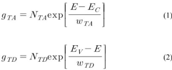
Fig. 2 shows the drain current (ID) characteristics as a function of gate bias voltage (VG). The active layer was a 50 nm oxide-semiconductor layer. As shown in Fig. 2, ID-VG curves were built well using the simulation model described in the previous section. Transfer curves depended on equilibrium electron-density (n0). As shown in the figure, a TFT with 1017 cm-3 n0 had a relatively large current at zero gate-bias.
[Fig. 2] Drain currents of TFTs with mono active layers as a function of gate bias voltage. The active layer thickness was 50 nm. Drain-source voltage was 10 V.
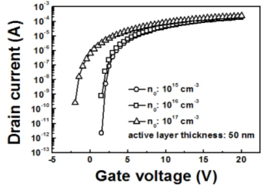
Fig. 3(a) shows μFE according to the thickness of the active layer. μFEs of TFTs with n0 of 1015 cm-3 and with n0 of 1016 cm-3 were similar to each other. However, a TFT with 1017 cm-3 n0 gave much less μFE. μFE
gradually decreased after a sharp initial drop as a function of increasing active layer thickness. As shown in the figure, the TFT with the thinner active layer showed higher field-effect mobility. The TFT with the 10 nm active layer showed the highest μFE. Especially for TFTs with high n0, a thin active layer should be used to obtain high μFE. Charge-density modulation of the upper side of the active layer became difficult as the active-layer
thickness increased due to the electric-field shield-effect of accumulated charges on the front side. This effect became severe for the case of high n0.
VTH showed the smallest absolute values for the 20 nm active-layers. For 1015 cm-3 n0 and 1016 cm-3 n0, VTH
variations as a function of active layer thickness were less than the 1017 cm-3 n0 case. As shown in Fig. 3(b), VTHs decreased noticeably when the active layer thickness increased from 10 nm to 20 nm. After this, VTHs increased in the positive direction as the active layer thickness increased. In the cases of these low carrier density active layers, the voltage drop at the source side between the top surface and the bottom surface of the active layer can be increased significantly due to the rather high resistivity of the active layer as the thickness of active layer increases. Therefore, larger positive voltage is needed to turn on TFTs having thicker active layer. For the 1017 cm-3 n0 case, VTH increased steeply to negative values with increasing active-layer thickness. This occurred because there were many electrons in the active layer with 1017 cm-3 n0; a larger negative voltage needs to be applied to the gate to deplete the channel as active-layer thickness increases. That is, VTH will become more negative as the thickness of the active layer increases.
The variation in SS is reported in Fig. 3(c). TFTs with n0 of 1015 cm-3 and 1016 cm-3 showed subthreshold swings that were nearly independent of the active-layer thickness and n0. For the case of 1017 cm-3 n0, subthreshold behavior could be divided into two regions. For the thinner-active-layer region under 170 nm, subthreshold behavior was similar to those of 1015 cm-3 n0 and 1016 cm-3 n0. For the thicker-active-layer region over 170 nm, SS showed higher values as the active layer thickness increased. This increase seemed to be related to electric-field shielding. When active-layer thickness was under 170 nm, SS was nearly independent of the active-layer thickness and n0.
[Fig. 3] Characteristics of TFTs with mono active layers as a function of the active layer thickness; (a) field-effect mobility (μFE), (b) threshold voltage (VTH), and (c) subthreshold swing (SS). Drain-source voltage was 10 V.
4. Double Active Layer
Fig. 4 shows ID-VG curves of TFTs with double active layers. The TFT structure was the same as that of the TFT with a mono active layer except for the active layer.
In this section, the active layer was composed of two layers with different n0. Fig. 4(a) shows results of TFTs with 50 nm thick active layers. The bottom-active-layer n0
and top-active-layer n0 were 1017 cm-3 and 1015 cm-3, respectively. The turn-on voltage showed a noticeable difference; however, on-current hardly changed between
TFTs with different bottom-active-layer thicknesses. Fig.
4(b) is the result of TFTs with 100 nm active layers; n0 of the bottom active layer was 1017 cm-3 and of the top active layer was 1015 cm-3 Switching performances became worse with thicker bottom active layers;
performance variation was larger than that of TFTs with 50 nm active layers. On-current increased slightly as the bottom active layer thickness increased. Fig. 4(c) gives results for TFTs with 50 nm thick active layers. The bottom active layer had 1015 cm-3 n0 and the top active layer had 1017 cm-3 n0. The turn-on voltage showed a noticeable difference and the on-current decreased slightly as the bottom active layer thickness increased. Fig. 4(d) shows results of TFTs with 100 nm thick active layers;
the n0 of the bottom active layer was 1015 cm-3 n0 and the n0 of the top active layer was 1017 cm-3. TFTs with thicker bottom active layers gave better switching performance though their performance variation was greater than that of TFTs with 50nm active layers. There was a noticeable decrease in on-current with increasing bottom-active-layer thickness. A comparison between TFTs with a higher n0 bottom active layer and lower n0 bottom active layer is shown in Fig. 5. On-currents were almost the same; however, the switching performance of a TFT with a higher n0 bottom active layer was better.
Fig. 6(a) shows μFEs of various TFTs. TFTs with bottom active layers of 1017 cm-3 n0 had better mobility in the low to medium thickness range of the bottom active layer. μFE of TFTs with bottom active layers of 1015 cm-3 n0 increased gradually according to the increase in bottom-active-layer thickness and then showed higher values for a thicker bottom active-layer. For the TFTs having 100 nm active layers, increase of μFE according to the increase of bottom layer thickness was significant for the case of bottom active layers of 1017 cm-3 n0. This can be understood considering the results of mono-active layer; the lower n0 active layer gave the higher μFE. TFTs with bottom active layers of 1015 cm-3 n0; thinner bottom means larger portion of top layer with 1017 cm-3 n0 causing lower μFE. Therefore, thicker bottom layer with 1015 cm-3 n0 makes layer μFE. For both cases of bottom active layer n0s, mobility increased when the total thickness of the active layer was lower due to ease of modulating the charge density of the thinner active layer.
[Fig. 4] Drain currents of TFTs with double active layers as a function of gate bias voltage. Drain-source voltage was 10 V.
[Fig. 5] Drain currents of TFTs with double active layers as a function of gate bias voltage; the layers with 1017 cm-3 n0 and 1015 cm-3 n0 had the same thickness (50 nm). The total thickness of the active layer was 100 nm. Drain-source voltage was 10 V.
Threshold voltage variations are shown in Fig. 6(b).
For TFTs with bottom active layers of 1017 cm-3 n0, VTHs decreased as bottom-active-layer thickness increased. For TFTs with bottom active layers of 1015 cm-3 n0, VTHs increased as the bottom active layer thickness increased.
TFTs with bottom active layers of 1017 cm-3 n0 with 50 nm active layers and with 100 nm active layers gave VTHs near 0 V for bottom active layer thicknesses of 40 nm and 70 nm, respectively. TFTs with bottom active layers of 1015 cm-3 n0 with 50 nm active layers and with 100 nm active layers gave VTHs near 0 V for bottom active layer thicknesses of 10 nm and 30 nm, respectively. As shown in the figure, VTH could be controlled by adjusting the thickness of the layer with 1017 cm-3 n0. As the thickness of the high n0 layer increased, more electrons appeared in the conduction channel even with an unbiased gate.
Therefore, VTH shifted negatively as a function of the increase in the thickness of the layer with 1017 cm-3 n0.
Fig. 6(c) shows subthreshold swings of TFTs with double active layers. SS showed little dependency on the bottom-active-layer thickness and n0. TFTs with the bottom active layer of 1015 cm-3 n0 and a total active-layer thickness of 100 nm showed more variation; however, all SS values in this figure were low enough for the TFTs to be used for FPDs.
In the case of the double active layer, better switching performances were obtained for TFTs with bottom active layers with 1017 cm-3 n0. This was because the bottom active layer with higher n0 caused higher electron density in the current path at the front channel; this produced a
higher on-current, and a top active layer with lower n0 was easier to deplete for the off state.
[Fig. 6] Characteristics of TFTs with double active layers as a function of the active layer thickness; (a) field-effect mobility (μFE), (b) threshold voltage (VTH), and (c) subthreshold swing (SS).
Drain-source voltage was 10 V.
4. Conclusions
Modeling was successful in producing transfer curves of OS-TFTs. Dependencies of TFT characteristics on active layer structure, active layer thickness, and equilibrium electron density were estimated. For mono-active-layer TFTs, thinner active layers produced higher field-effect mobility. VTH showed the smallest value for the 20 nm active-layer. Subthreshold swing
showed almost no dependence on active-layer thickness.
For the double-active-layer case, better switching performances were obtained for TFTs with bottom active layers with higher equilibrium electron-density. TFTs with thinner active layers had higher mobility. VTH shifted negatively with increasing layer thickness with higher equilibrium electron-density. Subthreshold swing showed almost no dependence on active-layer structure. These data will be beneficial for optimizing the structure, the thickness, and the doping ratio of the active layer of oxide-semiconductor TFTs.
References
[1] G. F. Bosen and J. J. Jacobs, "ZnO Field-Effect Transistor", Proc. IEEE, pp. 2094-2095, 1968.
[2] T. Hirao, M. Furuta, H. Furuta, T. Matsuda, T.
Hiramatsu, H. Hokari, M. Yoshida, H. Ishii and M.
Kakegawa, "Novel top-gate zinc oxide thin-film transistors (ZnO TFTs) for AMLCDs", J. Soc.
Information Display, vol. 15, pp. 17-22, 2007.
[3] P. Carcia, R. McLean and M. Reilly, "Oxide engineering of ZnO thin-film transistors for flexible electronics", J.
Soc. for Information Display, vol. 13, pp. 547-554, 2005.
[4] N. L. Dehuff, E. S. Kettenring, D. Hong, H. Q. Chang and J. J. Wager, “Transparent thin-film transistors with zinc indium oxide channel laer", Journal of Applied Physics. vol. 97, pp. 064505, 2005.
[5] W. B. Jackson, G. S. Herman, R. L. Hoffmann, C.
Taussig, S. Braymen, F. Jeffery and J. Hauschildt, "Zinc tin oxide transistors on flexible substrates", J.
Non-Cryst. Solids, vol. 352, pp. 1753-1755, 2006.
[6] K. Nomura, H. Ohta, K. Ueda, T. Kamiya, M. Hirano and H. Hosono, "All oxide transparent MISFET using high-k dielectrics gates", Microelectronic Engineering, vol. 72, pp. 294-298, 2004.
[7] K. Nomura, H. Ohta, A. Takagi, T. Kamiya, M. Hirano and H. Hosono, "Room-temperature fabrication of transparent flexible thin-film transistors using amorphous oxide semiconductors", Nature, vol. 432, pp.
488-492, 2004.
[8] H. Hosono, "Ionic amorphous oxide semiconductors:
Material design, carrier transport, and device application", J. Non-Cryst. Solids, vol. 352, pp.
851-858, 2006.
[9] J. K. Jeong, H. W. Yang, J. H. Jeong, Y. G. Mo and H. D. Kim, "Origin of threshold voltage instability in indium-gallium-zinc oxide thin film transistors", Appl.
Phys. Lett., vol. 93, pp. 123508, 2008.
[10] J. M. Lee, I. T. Cho, J. H. Lee and H. I. Kwon,
"Bias-stress-induced stretched-exponential time dependence of threshold voltage shift in InGaZnO thin film transistors", Appl. Phys. Lett., vol. 93, pp. 093504, 2008.
[11] I. Titkov, I. Pronin, I. Liniichuk and I. Grekhov,
"Transparent ferroelectric field effect transistors with a single-crystal SnO2 channel", Integr. Ferroelectr. vol. 72, pp. 53-60, 2005.
[12] D. Cho, Sh. Yang, C. Byun, J. Shin, M. Ryu, S. Park, C. Hwang, S. Chung, W. Cheong, S. Yoon and H. Chu,
"Transparent Al–Zn–Sn–O thin film transistors prepared at low temperature", Appl. Phys. Lett., vol. 93, pp. 142111, 2008.
[13] H. D. Kim, J. K. Jeong, Y. G. Mo and H. K. Chung,
"Oxide TFT as an Emerging Technology for Next Generation Display", Proc. Int. Meeting on Information Display, pp. 119-122, 2008.
[14] J. H. Lee, D. H. Kim, D. J. Yang, S. Y. Hong, K. S.
Yoon, P. S. Hong, C. O. Jeong, H. S. Park, S. Y. Kim, S. K. Lim, S. S. Kim, K. S. Son, T. S Kim, J. Y Kwon and S. Y. Lee, "World’s Largest (15-inch) XGA AMLCD Panel Using IGZO Oxide TFT", Soc.
Information Display 2008 Int. Symp. Digest of Tech.
Papers, pp. 625-628, 2008.
[15] ATLAS User’s Manual (Silvaco International, Santa Clara, California, 2007).
[16] A. Ohtomo, K. Tamura, K. Saikusa, K. Takahashi, T.
Makino, Y. Segawa, H. Koinuma and M. Kawasaki,
"Single crystalline ZnO films grown on lattice-matched ScAlMgO4(0001) substrates", Appl. Phys. Lett., vol. 75, pp. 2635-2637, 1999.
[17] K. B. Sundaram and A. Khan, "Work function determination of zinc oxide films", J. Vac. Sci. Technol.
A, vol. 15, pp. 428-430, 1997.
[18] Rode, D. L., Semiconductors and Semimetals, R. K.
Willardson and A. C. Beer, eds., Academic Press, N.Y., vol. 10, p. 1, 1975.
[19] H. H. Hsieh, T. Kamiya, K. Nomura, H. Hosono and C. C. Wu, "Modeling of amorphous InGaZnO4 thin film transistors and their subgap density of states", Appl.
Phys. Lett., vol. 92, pp. 133503, 2008.
[20] L. Bornstein, in Seimiconductors, edited by O.
Medelung (Springer, Berlin, 1998), vol III-17, pp.
35-115.
[21] P. Barquinha, A. Pimentel, A. Marques, L. Pereira, R.
Martins, E. Fortunato, “Effect of UV and visible light radiation on the electrical performances of transparent TFTs based on amorphous indium zinc oxide”, J.
Non-Cryst. Solids, vol. 352, pp. 1756- 1760, 2006.
[22] M. S. Grover, P. A. Hersh, H. Q. Chiang, E. S.
Kettenring, J. F. Wager and D. A. Keszler, "Thin-film transistors with transparent amorphous zinc indium tin oxide channel layer", J. Phys. D: Appl. Phys., vol. 40, pp. 1335-1338, 2007.
Ho-Nyeon Lee
[Regular member]• Aug. 1997 : Korea Advanced Instituted of Science and Technology, PhD in Physics.
• Aug. 1997 ~ Jun. 2001 : HYNIX, Research Engineer
• Jul. 2001 ~ Mar. 2004 : HYDIS Technology, Research Engineer
• Apr. 2004 ∼ Aug. 2006 : Samsung Advanced Institute of
Technology, Research Scientist
• Sep. 2006 ∼ current : Soonchunhyang Univ., Dept. of Display & Electronic Information Engineering, Professor
<Research Interests>
Information Display, Solar Energy