182
차량용 레이더를 위한 26GHz 40nm CMOS 광대역 가변 이득 증폭기 설계
26GHz 40nm CMOS Wideband Variable Gain Amplifier Design for Automotive Radar
최 한 웅*, 최 선 규*, 이 은 규*, 이 재 은*, 임 정 택*, 이 경 혁*, 송 재 혁*, 김 상 효*, 김 철 영*★
Han-Woong Choi*, Sun-Kyu Choi*, Eun-Gyu Lee*, Jae-Eun Lee*, Jeong-Taek Lim*, Kyeong-Kyeok Lee*, Jae-Hyeok Song*, Sang-Hyo Kim*, Choul-Young Kim*★
Abstract
In this paper, a 26GHz variable gain amplifier fabricated using a 40nm CMOS process is studied. In the case of an automobile radar using 79 GHz, it is advantageous in designing and driving to drive down to a low frequency band or to use a low frequency band before up conversion rather than designing and matching the entire circuit to 79 GHz in terms of frequency characteristics. In the case of a Phased Array System that uses time delay through TTD (True Time Delay) in practice, down conversion to a lower frequency is advantageous in realizing a real time delay and reducing errors. For a VGA (Variable Gain Amplifier) operating in the 26GHz frequency band that is 1/3 of the frequency of 79GHz, VDD : 1V, Bias 0.95V, S11 is designed to be <-9.8dB (Mea. High gain mode) and S22 < (Mea. high gain mode), Gain: 2.69dB (Mea. high gain mode), and P1dB: -15 dBm (Mea. high gain mode). In low gain mode, S11 is <-3.3dB (Mea. Low gain mode), S22 <-8.6dB (Mea. low gain mode), Gain: 0dB (Mea. low gain mode), P1dB: -21dBm (Mea. Low gain mode).
요 약
이 논문에서는 40nm CMOS 공정을 이용하여 제작된 26GHz 가변 이득 증폭기에 대한 연구를 수행하였다. 79GHz를 사용하는 자동차 레이더의 경우 주파수 특성상 회로 전체를 79GHz로 설계 및 매칭 하기 보다는 Down conversion 하여 낮은 주파수대역으로 구동하거나 Up conversion 전에 낮은 주파수 대역을 이용하는 것이 설계 및 구동에 유리하다.
실제적으로 TTD(True Time Delay)를 통해 시간지연을 이용하는 Phased Array System 의 경우에도 현재 기술로는 낮은 주파수로 Down conversion하는 것이 오차를 줄이고 실제적 시간지연을 구현하는데 좋다. 79GHz 주파수의 1/3인 26GHz 주파수 대역에서 동작하는 VGA(Variable Gain Amplifier)에 대하여 설계하였고 1-stage의 cascode amplifier 형태로 구성된 회로에서 VDD : 1V, Bias 0.95V, S11은 < -9.8dB(Mea. High gain mode), S22 <-3.6dB(Mea. High gain mode), Gain : 2.69dB(Mea. High gain mode), P1dB : -15 dBm (Mea. High gain mode) 로 설계되었다. Low gain mode 에서는 S11은 < -3.3dB(Mea. Low gain mode), S22 < -8.6dB(Mea. Low gain mode), Gain : 0dB(Mea. Low gain mode), P1dB : -21 dBm (Mea. Low gain mode)로 설계되었다.
Key words : Variable Gain Amplifier, Phased Array, Automobile, Cascode Amplifier, Up conversion, Down conversion, Gain control
* Dept. of Electronics Engineering, Chungnam National University
★Corresponding author
E-mail: [email protected], Tel: +82-42-821-5663
※ Acknowledgment
This work was supported by research fund of Chungnam National University.
Manuscript received Jun. 12, 2018; revised Jun. 22, 2018; Accepted Jun. 25, 2018
This is an Open-Access article distributed under the terms of the Creative Commons Attribution Non-Commercial License (http://creativecommons.org/licenses/by-nc/3.0) which permits unrestricted non-commercial use, distribution, and reproduction in any medium, provided the original work is properly cited.
Ⅰ. 서론
최근 자동차의 안전시스템은 기계적인 체계에 따 라 움직이던 기존의 시스템에서 좀 더 정교하게 반응할 수 있고 소형화가 가능한 전자시스템으로 변화하고 있다. 이는 차량 주행 중 목표물의 정밀 한 탐지가 가능한 밀리미터파를 사용한 센서를 사용하는 것이 유리하고 이러한 밀리미터파 회로 들을 높은 집적도를 통해 시스템을 하나의 칩에 담아내는 효율적인 생산이 가능해졌기 때문이 다.[1][2]
79GHz 대역의 주파수는 자동차 주행시 작은 목표물을 탐지해 내는데 적합한 짧은 파장을 가지 고 있다. 그러나 이러한 고주파는 직진성이 높고 주변 유닛과의 커플링이 쉬워 저주파에 비해 작은 Electromagnetic 구조 하나에도 민감하게 반응하기 때문에 회로를 구성하는데 있어 상당한 정교함이 요구된다. 이렇듯 79GHz대역의 주파수로 회로 전체를 매칭하여 사용하는 것은 매우 어렵기 따르 기 때문에 79GHz대역의 주파수를 직접 수신하는 저잡음 증폭기, 송신하는 전력증폭기 이외의 회로 내에서는 낮은 주파수를 통해 구동하는 편이 유리 하다. 주파수 변환은 Mixer를 사용하여 Down conversion 하거나 Mixer의 Up conversion 또는 Multiplier의 주파수 체배를 통해 이루어진다.
[3][4]
RF회로는 입력에 너무 강한 신호가 들어오게 되면 각 회로간의 입/출력 가능한 이득범위를 넘어 서 비선형적인 특성이 나타나거나 회로가 고장날 우려가 있다. 따라서 너무 강한 신호의 경우 이득 을 낮추어주는 회로가 필요한데 가변이득증폭기는 증폭기에 흐르는 전류를 전압 신호를 통해 조정하 여 필요시 이득을 낮추어 줄 수 있다.[5][6]
본 논문에서는 79GHz 대역의 주파수를 사용하 는 회로에서 3배 주파수를 체배하기 전인 26GHz 대역의 가변이득증폭기를 40nm CMOS 공정을 이용해 설계하였다.
Ⅱ. 가변이득증폭기 설계
이 논문의 가변이득증폭기(Variable Gain Amplifier)는 Fig. 1.과같이 1-stage Cascode
Fig. 1. 1-Stage Cascode Variable Gain Amplifier Schematic 그림 1. 1단 Cascode 가변이득증폭기 회로도
Amplifier 로 구성되었으며 Common gate의 current를 steering 하여 gain을 줄이는 구조로 설
계되었다. 그림 1.에서 보이는 바와 같이
Common gate amplifier의 Gain control Transistor가 Digital 신호(1 또는 0)에 응답 하여 0일 때 High gain mode, 1일 때 Low gain mode 로 동작한다.
설계된 회로에서 트랜지스터의 이득은 M1의 gm1과 M1의 출력저항 Ro1에 M2의 Gm2와 출력 저항 Ro2에 의해 결정된다. Low gain mode에서 는 M3의 Ro3에 의해 출력저항이 Ro2//Ro3 로 낮아지게 되어 이득을 조절할 수 있다.
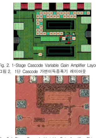
Fig. 2. 1-Stage Cascode Variable Gain Amplifier Layout 그림 2. 1단 Cascode 가변이득증폭기 레이아웃
Fig. 3 1-Stage Cascode Variable Gain Amplifier Chip 그림 3. 1단 Casocde 가변이득증폭기 칩 사진
Ⅲ 측정결과
Fig. 4 S11 (Input Returen Loss – High Gain Mode) 그림 4. 입력 반사 손실
Fig. 5 S22 (Output Returen Loss – High Gain Mode) 그림 5. 출력 반사 손실
Fig. 6 S21 (Gain – High Gain Mode) 그림 6. 이득
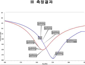
Fig. 4, 5, 6 은 High gain mode에서의 시뮬레이션 결과와 측정 결과를 비교한 그래프이다. 입력 반사 손실인 S11은 < -9.8dB(Mea. High gain mode)이 며 출력반사손실인 S22는 <-3.6dB(Mea. High gain
mode)이다. 이득은 : > 2.69dB(Mea. High gain mode), P1dB : -15 dBm (Mea. High gain mode) 로 설계되었다.
Fig. 7 S11 (Input Returen Loss – Low Gain Mode) 그림 7. 입력 삽입 손실
Fig. 8 S22 (Output Returen Loss – Low Gain Mode) 그림 8. 출력 삽입 손실
Fig. 9 S21 (Gain – Low Gain Mode) 그림 9. 이득
Fig 7, 8, 9는 Low gain mode 에서의 시뮬레이션 결과와 측정 결과를 비교한 그래프이다. 입력반사손 실인 S11은 < -3.3dB(Mea. Low gain mode)이며,
출력반사손실인 S22는 < -8.6dB(Mea. Low gain mode)이다. 이득은 Gain : >0dB(Mea. Low gain mode), P1dB : -21 dBm (Mea. Low gain mode) 로 설계되었다.
Table 1. Comparison of gain mode 표 1. 이득 모드에 따른 성능 비교
Parameters High gain mode Low gain mode Input return loss < - 9.8 dB < -3.3 dB Output return loss < - 3.6 dB < - 8.6 dB
Channel bandwidth 5 GHz 5 GHz
VGA gain > 2.68 dB >0 dB
P1dB -15 dBm -21 dBm
chip size 550 x 438 um^2
Ⅳ 결론
본 논문의 가변 이득 증폭기는 40nm CMOS 공정을 이용하여 1-stage cascode 형태로 설계되 었다. 설계결과 입출력단 Inductor의 inductance가 설계치보다 낮아져 매칭이 높은 주파수로 이동하 는 결과를 나타내었지만 전체적인 파형이 유지되 고 전압 신호에 따라 이득이 조절되는 것을 확인 할 수 있었다. 입력 반사 손실(S11)은 : -9.8dB / -3.3dB 이고 출력 반사 손실은(S22)은 : -3.6dB / -8.6dB 이다. Gain은 2.69dB / 0 dB 로 넓은 범위 에서 동작하며 약 3dB Gain control이 가능하다.
References
[1] J. W. May and G. M. Rebeiz, “Design and characterization of WbandSiGe RFICs for passive millimeter-wave imaging,” IEEE
Trans. Microw. Theory Tech., vol. 58, no. 5, pp.
1420–1430,
2010.DOI:10.1109/TMTT.2010.2042857 [2] A. Tomkins, P. Garcia, and S. P.
Voinigescu, “A passive W-band imaging receiver in 65-nm bulk CMOS,” IEEE J.
Solid-State Circuits, vol. 45, no. 10, pp.1981–1991, 2010.
DOI:10.1109/JSSC.2010.2058150
[3] D.L Lu et al, “A 75.5-to-120.5-GHz, High-gain CMOS Low-Noise Amplifier” in IEEE MTT-S Int. Microwave Symp.
Dig., pp. 1–3, 2012.
DOI:10.1109/MWSYM.2012.6259481 [4] Donghyup Shin, Choul-Young Kim, Dong-Woo Kang and Gabriel M. Rebeiz, “A High-Power Packaged Four-Element
X-band Phased-Array Transmitter in 0.13um CMOS for Radar and Communication Systems,”
” in IEEE MTT-S Vol 61, No. 8,pp. 3060-3071, 2013.DOI:10.1109/TMTT.2013.2271488
[5] Sang Young Kim, Ozgur Inac, Choul-Young Kim, Donghyup Shin and Gabriel M. Rebeiz, “A 76-84 GHz 16-Element Phased Array Receiver with a Chip-Level Built-In Self-Test System,”
” in IEEE MTT-S S Vol 61, No. 8, pp.3083-3098,
2013.DOI:10.1109/TMTT.2013.2265016
[6] Choul-Young Kim, Dongwoo Kang, Gabriel M. Rebeiz, “A 44-46 GHz 16-Element SiGe BiCMOS High-Linearity Transmit/Receive Phased Array,” in IEEE MTT-S S Vol 60, No. 8, pp. 730-742,
2013.DOI:10.1109/TMTT.2012.2184130
BIOGRAPHY
Han-Woong Choi (Member)
2017 : BS degree in Electrical Engineering, Chungnam National University.
2017~ : Course of MS in Electronics Engineering, Chungnam National university.
Sun-Kyu Choi (Member)
2002 : BS degree in Electrical Engineering, Korea Advanced institute of Science and Technology(KAIST).
2004 : MS degree in Electrical Engineering, KAIST.
2009 : PhD degree in Electrical Engineering, KAIST.
2009~2010 : Postdoctoral Research Fellow, in Electrical Engineering, KAIST.
2011~2014 : Senior Engineer, in Samsung Electronics 2017~ : Senior Engineer, in RFpia
Eun-Gyu Lee (Member)
2004 : BS degree in Electronics Engineering, Chungnam National University.
2006 : MS degree in Pohang University of Science and Technology (Postech).
2006~2009 : Engineer, Samsung Electronics.
2012~ : Ph.D. student, in Electronics Engineering, Chungnam National University.
Jae-Eun Lee (Member)
2016 : BS degree in Electronics Engineering, Chungnam National University.
2016~ :Course of PhD degree in Science in Electrinics, Radio Sciences & Engineering and Information Communications Engineering, Chungnam National University.
Jeong-Taek Lim (Member)
2016 : BS degree in Electronics Engineering, Chungnam National University.
2018 : MS degree in Science in Electrinics, Radio Sciences
& Engineering and Information Communications Engineering, Chungnam National University.
2018~ : Course of PhD degree in Science in Electrinics, Radio Sciences & Engineering and Information Communications Engineering, Chungnam National University.
Jae-Hyeok Song (Member)
2018 : BS degree in Electrical Engineering, Chungnam National University.
2018~ : Course of MS in Electronics Engineering, Chungnam National university.
Sang-Hyo Kim (Member)
2018 : BS degree in Electrical Engineering, Chungnam National University.
2018~ : Course of MS in Electronics Engineering, Chungnam National university.
Choul-Young Kim (Member)
2002 : BS degree in Electronics Engineering, Chungnam National University.
2004 : MS degree in Electrical Engineering, Korea Advanced Institute of Science and Technology (KAIST) 2008 : PhD degree in Electrical Engineering, Korea Advanced Institute of Science and Technology (KAIST)
2009~2011 : Postdoctoral Research Fellow, in Electrical and California, San Diege (UCSD) 2011 ~ : Associate Professor, In Electronics Engineering, Chungnam National University.