Regular Paper
190
J. KIEEMEVol. 26, No. 3, pp. 190-193, March 2013
DOI: http://dx.doi.org/10.4313/JKEM.2013.26.3.190
80 V급 저전력 반도체 소자의 관한 연구
심관필1, 안병섭1, 강예환1, 홍영성1, 강이구1,a
1 극동대학교 에너지반도체학과
Design of 80 V Grade Low-power Semiconductor Device
Gwan pil Sim
1, Byoung Sup Ann
1, Ye Hwan Kang
1, Young Sung Hong
1, and Ey Goo Kang
1,a1 Department of Materials Engineering, Far East University, Eumseong 369-700, Korea
(Received January 22, 2013; Accepted February 24, 2013)
Abstract: Power MOSFET and Power IGBT is develop in power savings, high efficiency, small size, high reliability, fast switching, low noise. Power MOSFET can be used high-speed switching transistors devices. Power MOSFET is devices the voltage-driven approach switching devices are design to handle on large power, power supplies, converters. In this paper, design the 80V MOSFET Planar Gate type, and design the Trench Gate type for realization of low on-resistance. For both structures, by comparing and analyzing the results of the simulation and characterization.
Keywords: Power MOSFET, Planer gate MOSFET, Trench gate MOSFET, On-resistance
1. 서 론1)
Power MOSFET (metal oxide semiconductor field effect transistor)는 전압 구동 방식으로 동작하는 소 자이며, 고전압, 고전류를 처리하기 위해 설계된 스위 칭 디바이스로서 전원 공급 장치, 변환기 등에 널리 사용된다. 모터 구동에 사용되는 power MOSFET는 낮은 온 저항을 가지기 때문에 동작 상태에서 전력 전달 손실을 줄여줌으로써 효율을 높일 수 있으며, 결과적으로 저전력 구현을 가능하게 한다.
본 연구에서는 80 V급 power MOSFET의 planar gate type 및 trench gate type의 소자를 설계하고 각 각의 구조에 대해 simulation을 진행하였다.
a. Corresponding author; [email protected]
Copyright ©2013 KIEEME. All rights reserved.This is an Open-Access article distributed under the terms of the Creative Commons Attribution Non-Commercial License (http://creativecommons.org/licenses/by-nc/3.0) which permits unrestricted non-commercial use, distribution, and reproduction in any medium, provided the original work is properly cited.
Simulation은 Sysnopsys사에 T-CAD를 사용하였 으며, 각 simulation은 항복 전압 및 온 저항 특성을 분석하였으며, 분석 결과를 바탕으로 고내압 · 저전력 에 최적화된 power MOSFET를 설계하고자 하였다.
2. 실험 방법
그림 1은 planer gate MOSFET 구조와 trench gate MOSFET 구조를 나타내고 있다. 이번 연구를 위하 여 기본적인 구조의 MOSFET를 설계하였고, planer 구조를 완성한 후에 planer의 특성과 같은 항복전압 과 작은 cell size의 낮은 온-상태 전압 강하를 갖는 구조의 trench gate MOSFET를 설계하였다. Planer 타입의 설계하기 위해서 항복전압을 위해서 항복전압 의 가장 큰 영향을 주는 Epi 층의 크기와 Epi의 농도 의 따른 시뮬레이션을 진행하여 항복전압과 온-상태 전압강하의 트레이드 오프관계를 확인하였고, P-base 의 크기와 농도의 따른 문턱전압 특성을 확인하였다.
전기전자재료학회논문지, 제26권 제3호 pp. 190-193, 2013년 3월: 심관필 등 191
(a) (b)
Fig. 1. MOSFET structure in general. (a) planer MOSFET, (b) trench MOSFET.
2.1 Planer Gate type MOSFET 설계
항복전압 및 기타 특성에 가장 큰 영향을 미치는 요소인 N-드리프트 영역의 농도는 MOSFET 소자의 Epi 층으로 내압을 정하는데 가장 중요한 영향을 미 치는 부분이기 때문에 Epi의 농도에 따른 시뮬레이션 을 실험해 보았다. 다음 그림은 Epi 농도를 4E15~
6E15까지 변화에 따른 항복전압과 온 상태 전압강하 를 알아보기 위한 실험이다.
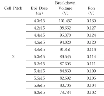
Table 1. Epi dose by breakdown voltage and Ron.
Cell Pitch Epi Dose (㎠)
Breakdown Voltage
(V)
Ron (V)
2
4.0e15 101.457 0.130
4.2e15 98.662 0.127
4.4e15 96.370 0.124
4.6e15 94.020 0.120
4.8e15 91.851 0.116
5.0e15 89.545 0.114
5.2e15 87.303 0.111
5.4e15 84.869 0.109
5.6e15 82.692 0.106
5.8e15 80.706 0.104
6.0e15 78.784 0.102
Fig. 2. Epi dose by breakdown voltage and Ron.
항복전압을 결정하기 위해서 다른 변수는 고정 후 Epi 농도를 4.0E15∼6.0E15까지 변화시켜 실험을 진 행하였다. 실험 결과 그림 2와 같이 Epi 농도가 높아 짐에 따라 저항은 낮아지지만 항복전압 또한 낮아지 는 현상을 확인할 수 있었다. 즉, Von drop과 breakdown voltage는 서로 트레이드 오프 관계를 확 인할 수 있었다.
위 실험을 통해 본연구의 목표인 80V급을 설계하 기 위하여 시뮬레이션 오차를 20%로 선정하고 Epi dose는 4.2E15를 선택하여 다음 실험을 진행하였다.
다음 실험은 문턱전압을 결정하기 위해서 Epi dose 를 4.2E15로 고정 후 P-Base의 농도를 변환하여 진 행을 하였다.
Table 2. P-Base dose by Vth.
Epi Dose (㎠)
P-Base Dose (㎠)
Vth (V)
4.2e15
1.00e13 0.86171
1.25e13 1.21612
1.50e13 1.67477
1.75e13 2.03614
2.00e13 2.4114
2.25e13 2.8005
2.50e13 3.13412
2.75e13 3.43294
3.00e13 3.75956
192 J. KIEEME, Vol. 26, No. 3, pp. 190-193, March 2013: G. Sim et al.
Fig. 3. P-Base dose by Vth.
문턱전압을 결정하기 위해서 다른 변수는 고정 후 P-Base 농도를 1.0E13∼3.0E13까지 변화시켜 실험을 진행하였다. 실험 결과 그림 3과 같이 P-Base 농도가 높아짐에 따라 gate 밑 채널의 영향을 받아 문턱전압 이 변화하는 것을 확인할 수 있었다.
2.2 Trench gate type MOSFET 설계
Trench gate type MOSFET의 설계는 planer gate type MOSFET의 특성인 항복전압과 문턱전압을 같 게 설계하기 위해서 planer 타입의 BV와 Vth의 특성 파라미터를 같게 설계를 하였다.
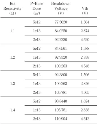
다음 실험은 trench gate type MOSFET의 BV와 Vth를 조절하기 위해서 Epi 비저항 (resistivity)과 P-Base 농도를 변수로 하여 실험을 진행하였다.
Fig. 4. Epi resistivity and Pbase dose by BV.
Table 3. Epi resistivity and Pbase dose by BV, Vth.
Epi Resistivity
(Ω)
P-Base Dose
(㎠)
Breakdown Voltage
(V)
Vth (V)
1.1
5e12 77.5620 1.504
1e13 84.0250 2.874
2e13 92.2230 4.520
1.2
5e12 84.6561 1.588
1e13 92.9320 2.838
2e13 100.263 4.548
1.3
5e12 92.3800 1.596
1e13 100.263 2.846
2e13 105.781 4.505
1.4
5e12 98.8440 1.624
1e13 105.781 2.838
2e13 110.904 4.512
Fig. 5. Epi resistivity and Pbase dose by Vth.
실험 결과 planer type과 동일하게 비저항의 값이 커질수록 breakdown voltage가 증가하는 것을 확인 하였고 본 실험을 통해서 planer type의 특성 파라미 터를 같게 설계하기 위해서는 동일한 BV와 Vth를 선 택하여 진행하였다.
전기전자재료학회논문지, 제26권 제3호 pp. 190-193, 2013년 3월: 심관필 등 193
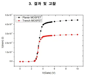
3. 결과 및 고찰
Fig. 6. Planer type and trench type by Vth.
Fig. 7. Planer type and trench type by BV.
Fig. 8. Planer type and trench type by Von drop.
Table 4. Epi resistivity and Pbase dose by BV, Vth.
Section V
TH(V)
BV (V)
Von drop (V)
Cell Size (㎛) Planer
IGBT 2.800 98.5796 0.124 2
Trench
IGBT 2.846 100.263 0.122 1
Perfor- mance
50%
down
4. 결 론
시뮬레이션을 통해서 80 V급 planer MOSFET와 trench MOSFET를 설계하여 비교 분석을 하였다. 드 리프트 영역의 비저항에 따라서 드리프트 저항력으로 인하여 항복전압과 온-상태 전압 강하 간에 관계를 확인하였다. 비교 결과 planer 구조에서 항복전압과 문턱전압은 동일한 조건이고 cell size가 2 ㎛에서 1
㎛로 50%가 감소했지만 온-상태 전압강하는 동일하 게 나오는 것을 확인할 수 있었다.
감사의 글
본 논문은 2012년도 전력반도체 소자 설계 가이드 개발 사업으로 진행되었습니다.
REFERENCES