저전력 무선통신 모뎀 구현용 전류기억소자 성능개선
김성권*
Performance Improvement of Current Memory for Low Power Wireless Communication MODEM
Seong-kweon Kim*
요 약
다양한 무선통신 방식이 출현함에 따라, 배터리 수명과 저전력 동작이 중요시되면서 무선 통신용 LSI는 SI circuit을 이용하는 analog current-mode signal processing을 주목하고 있다. 그러나 SI (Switched-Current) circuit을 구성하는 current memory는 clock-feedthrough의 문제점을 갖는다. 본 논문에서는 current memory의 문제점인 clock-feedthrough의 일반적인 해결방안으로 CMOS switch의 연결을 검토하고, current memory 성능 개선의 설계방안을 제안하기 위하여 CMOS switch 간의 width의 관계를 도출하고자 한다. Simulation 결과, memory MOS의 width가 20um, input current와 bias current의 ratio가 0.3, CMOS switch nMOS의 width가 2~6um일 경우에 CMOS switch 간의 width는 의 관계로 정의되고, CMOS switch nMOS의 width가 6~10um일 경우에 CMOS switch 간의 width는 의 관계로 정의되는 것을 확인하였 다. 이 때 정의된 MOS transistor의 관계는 memory MOS의 성능향상을 위한 설계에 유용한 지침이 될 것으 로 기대된다.
ABSTRACT
It is important to consider the life of battery and low power operation for various wireless communications. Thus, Analog current-mode signal processing with SI circuit has been taken notice of in designing the LSI for wireless communications.
However, in current mode signal processsing, current memory circuit has a problem called clock-feedthrough. In this paper, we examine the connection of CMOS switch that is the common solution of clock-feedthrough and calculate the relation of width between CMOS switch for design methodology for improvement of current memory. As a result of simulation, when the width of memory MOS is 20um, ratio of input current and bias current is 0.3, the width relation in CMOS switch is obtained with
, for the nMOS width of 2~6um in CMOS switch. And from the same simulation condition, it is obtained with for the nMOS width of 6~10um in CMOS switch. Then the defined width relation of MOS transistor will be useful guidance in design for improvement of current memory.
키워드
SI(Switched-Current) Circuit, Analog Current-mode Signal, Current Memory, Clock-Feedthrough
* 목포해양대학교 해양전자통신공학부 접수일자 : 2008. 04. 19 심사완료일자 : 2008. 05. 27
Ⅰ. 서 론
현대사회는 유비쿼터스 센서 네트워크 (USN : Ubi- quitous Sensor Network)의 실현을 위해 음성·사진·동 영상 등의 멀티미디어 통신의 수요가 급증하였고, 다양 한 통신 방식이 활발히 연구되어 왔으며 그 결과, 다양 한 무선통신방식이 출현하게 되었다. 무선통신의 큰 쟁 점은 통신의 지속성과 이동성이다. 이를 보장받기 위해 서는 통신시스템이 저전력으로 동작하여야 하며, 따라 서 저전력 동작이 가능한 무선통신용 LSI (Large Scale Integrated Circuit)의 구현이 필요하다. 무선통신시스템 을 구현하기 위해서 기본적으로 신호처리 (signal processing)가 필요하며, 신호처리는 digital voltage -mode signal processing과 analog current-mode
VDD
M1 M2
Out
i2 -k(i1+i2)
I I
I+i1+i2
1:K i1
K(I+i1+i2) Summation
point
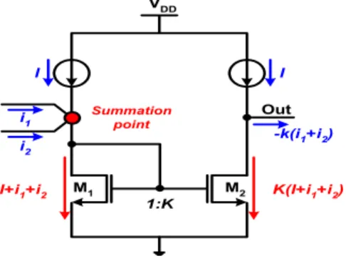
그림 1. Gate width-ratio current mirror Fig. 1 Gate width-ratio current mirror
signal processing이 있다. Digital voltage-mode signal processing은 신호처리의 정확도면에서는 우수한 성능 을 갖고 있지만, voltage operational amplifier로 동작하 는 SC (Switched -Capacitor) circuit으로 구현되기 때 문에 주파수 대역이 높아짐에 따라 높은 전력을 요구하 는 단점을 갖고 있다. 반면 analog current-mode signal processing은 current mirror로 동작하는 SI(Switched -Current) circuit으로 구현되며, 이는 초기에 설정된 bias voltage로만 동작되기 때문에 전력의 변동이 거의 없다. 그러므로 주파수 대역이 높아지더라도 전력을 유 지하기 때문에 저전력 동작이 가능하다. 따라서 통신시 스템의 저전력 동작을 위한 신호처리로 analog cur- rent-mode signal processing을 주목하게 되었다[1].
Analog current-mode signal processing의 구현을
위해서는 신호처리의 기본동작인 summation, signal Inversion, scaling, memory가 요구되며, current mirror 와 SI circuit으로 구현됨으로써, analog current-mode signal processing이 가능하다[2].
그러나 memory 동작을 구현하는 SI circuit은 cu- rrent memory로 구성되고, 이 current memory는 MOS (Metal-Oxide Semiconductor)로 설계되기 때문에, tran- sistor의 비선형적인 동작과 threshold voltage (Vt) 등과 같은 공정상의 mismatch에 의해 harmonic distortion이 나타나고, current memory의 성능을 저하시키는 clock- feedthrough의 문제점이 발생한다. 이 문제점을 최소화하 기 위한 방안으로는 일반적으로 CMOS switch의 사용이 제안되고 있다[3].
CMOS switch를 연결한 current memory는 차세대 무선통신기술로 주목받고 있는 OFDM(Orthogonal Fr- equency Division Multiplexing)용 FFT (Fast Fourier Transform) 프로세서 및 저전력 동작을 위한 무선기기 등에 광범위하게 적용될 수 있다. 따라서 THD (Total Harmonic Distortion)의 절감을 고려하여
VDD
M1 M2
iin
J J
SW1 SW1
SW2
J+iin
Vgs1 Vgs2 Cgs
그림 2(a). SI circuit의 track mode Fig. 2(a) Track mode of SI circuit
VDD
M1 M2
iin
J J
SW1 SW1
SW2
I
Vgs1 Vgs2 Cgs
그림 2(b). SI circuit의 hold mode Fig. 2(b) Hold mode of SI circuit
VDD
M1 M2
iin
J J
SW1
SW1
SW2
Vgs1 Vgs2 Cgs
J+iout
=J+iin iout
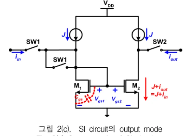
그림 2(c). SI circuit의 output mode Fig. 2(c) Output mode of SI circuit
current memory의 성능을 개선하고, 이를 범용적으로 설계하기 위한 설계 지침에 대한 연구가 필요하다.
본 논문에서는 clock-feedthrough 현상을 최소화하 고자 CMOS switch를 연결한 current memory를 설계 하고, THD를 절감시키기 위해 input signal과 bias current의 ratio를 결정하여 CMOS switch 간의 width 관계를 도출함으로써, current memory의 성능 개선을 위한 설계 지침을 제안한다.
Ⅱ. SI (Switched-Current) circuit 2.1 Analog Current-mode signal processing
신호처리는 digital voltage-mode signal processing과 analog current-mode signal processing이 있다. 이 때 통 신시스템의 저전력 동작을 위한 신호처리로 analog current-mode signal processing이 주목되었고, 이를 구 현하기 위하여 신호처리의 기본동작이 요구된다.
신호처리의 기본동작으로는 summation, signal In- version, scaling, memory가 있다. 각 신호처리의 동작 을 analog current-mode signal processing에서 구현하 기 위하여, summation, signal inversion, scaling 동작 은 그림 1과 같은 gate width-ratio current mirror를 이용하고, memory 동작은 SI circuit에 의해 구현된다 [2].
그림 1과 같이 입력 노드에 전류 (i1, i2)를 입력하면, summation point에서 i1, i2를 합한 전류 값이 입력됨으 로써 summation 동작을 한다. 이 때, 입력 노드에 입력
되는 전류 합의 최대값이 bias current 보다 작아야 한 다. 또한 current mirror는 출력 단의 다음 단에서 입력 신호와 동일한 신호를 끌어오기 때문에 입력 신호와 크 기는 같지만 방향은 반대인 신호가 출력된다. 즉, 입력 신호가 (i1+i2)이므로 출력 신호는 -(i1+i2)로 입력 신호 의 inversion 동작임을 확인할 수 있다. Scaling 동작은 gate width-ratio current mirror의 M1과 M2의 aspect ratio factor (W1/L1 : W2/L2 [K])에 따른다. 그림 1에서 보는 것과 같이 M1의 drain-source current (Ids1)가 식 (1)과 같다면, M2의 Ids2는 K에 따라 식 (2)와 같다. 즉, 입력 신호가 K배만큼 출력되는 scaling 동작을 한다.
(1)
(2)따라서 analog current-mode signal processing으로 신호처리의 기본동작의 구현이 가능함을 확인할 수 있다.
2.2 SI (Switched-Current) circuit의 기본원리
SI circuit의 memory 동작은 current memory의 current track/hold (T/H) mode에 의해 구현된다. 그림 2는 current memory의 T/H 동작이다. Track mode (SW1 ON, SW2 OFF)일 경우, memory MOS (M1)의 drain-source current (ids)는 input current (iin)와 bias current (J)가 합해진 iin+J의 전류가 흐르고, M1의 gate-source voltage (Vgs)은 iin+J의 전류가 흐를 수 있을 만큼의 전압이 걸린다. 이 때, 출력 신호는 출력 단의 다음 단에서 iin과 동일한 크기의 신호를 끌어옴으 로써, 출력 신호는 iout=-iin과 같다. 또한 M1의 gate-source 사이의 parasitic capacitor (Cgs)에 Vgs 만
Mm Ms
Vclk Cgd
Cgs Vgs
Mm
Cgd Cgs Vgs Clock
Feedthrough
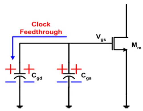
그림 3. Current memory의 clock-feedthrough Fig. 3 Clock-feedthrough of current memory
큼의 전하를 저장한다. Hold mode (SW1, SW2 OFF) 에서는 input current (iin)가 입력되지 못하고 M1에 bias current (J)만 흐르지만, M1의 gate-source 사이의 parasitic capacitor (Cgs)에 Vgs만큼의 전하를 유지한다.
지연시간 후, SW2가 ON되면 Cgs에 저장된 Vgs에 의해 track mode의 출력 전류와 같은 신호가 흐르게 된다.
즉, SI circuit은 지연시간동안 입력신호를 저장한 후 출 력시키는 memory 동작을 수행한다[3].
그러나 current memory는 switch의 ON/OFF에 의 해 동작하기 때문에 switch의 parasitic capacitor로부터 clock-feedthrough와 같은 문제점이 발생한다.
Ⅲ. Clock Feedthrough와 해결방안 3.1 Clock Feedthrough
Clock-feedthrough는 memory MOS(Mm)의 gate에 연결된 스위치가 OFF되었을 때, Mm의 capacitive node 에 저장된 전하가 스위치의 parasitic capacitor에 누설 되는 현상이다. 그림 3은 current memory의 clock- feedthrough를 나타낸 것으로, Mm은 memory MOS, Ms는 스위치 MOS, Cgs는 Mm의 gate-drain 사이에 존 재하는 parasitic capacitor, Cgd는 Ms의 parasitic capacitor이다.
Current memory는 Ms가 ON (Vclk : High)일 때, track mode로 동작하지만, OFF (Vclk : Low)일 경우, 그림 3과 같이 Cgd는 ground에 연결된 것과 같아지므 로 Cgs와 병렬연결된 것처럼 보인다. 따라서 Cgs에 저장
되어 있는 전하가 Cgd로 누설되는 현상이 생기고, 식 (3)과 (4)와 같이 Mm의 Vgs를 변동시키게 된다. 따라서 입력전류를 지연시간동안 저장하는데 문제가 발생하고, current memory의 성능을 저하시키게 된다.
∙
∙′ (3)′
∙ (4)
3.2 Clock Feedthrough의 해결방안
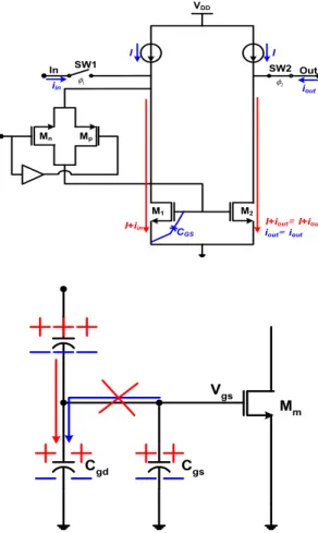
Clock-feedthrough는 switch의 parasitic capacitor에 의해 memory MOS의 Vgs를 변동 시키는 문제점을 가 지고 있다. 이를 해결하는 방법으로 일반적으로 CMOS switch의 연결이 있다. 따라서 CMOS switch의 연결을 검토하였다. 그림 4와 같이 CMOS switch를 연결함으 로써, Ms가 전하를 끌어당기는 현상을 방지하도록 하 였다. 즉, Ms의 parasitic capacitor로 누설되는 전하를 M4가 상쇄시켜서 M2의 Vgs를 유지하게 한다.
본 논문은 clock-feedthrough의 해결을 위해 CMOS switch의 연결을 검토하였고, 0.25um process로current memory를 제작하기 위하여 switch와 CMOS switch의 적절한 width 값의 관계를 도출하고자 한다.
Ⅳ. CMOS switch를 연결한 current memory의 width 관계 도출 4.1 Simulation parameter 설정
CMOS switch를 연결한 current memory의 성능개 선을 위한 설계방안을 제안하기 위하여 CMOS switch 의 width 관계를 도출할 필요가 있다. 따라서 위해 설 정할 parameter는 input current (i)와 bias current (J) 의 ratio (i/J), 전류원을 구성하는 pMOS의 width와 memory MOS인 nMOS width, delay time이 있다.
∙ ∆
∙∙ ∆∙ ∆
∙∙ ∆
∙∙ ∆
∙ sin
∙∙ ∆cos ⋯
(5)
Input current (i)와 bias current (J)의 ratio (i/J)는 current mirror의 threshold voltage mismatch (⧍Vt)를 고려하여 설정된다. threshold voltage mismatch에 의 해 offset current는 식 (5)와 같고, 이 offset current를 감
VDD
M1 M2
In Out
iin iout
I I
I+iin I+iout= I+iout
SW1 SW2
φ1 φ2
iout= iout CGS
Mn Mp
Mm
Cgd Cgs Vgs
그림 4. CMOS switch를 연결한 current memory Fig. 4 Current memory with CMOS switch
소시키기 위해 셋째 항인 harmonic distortion을 절감시 켜줄 필요가 있다. Harmonic distortion은 i와 J의 ratio (MI)와 밀접한 관계를 갖고 있기 때문에 이 MI을 적절 하게 설정해야 한다. 따라서 total harmonic distortion (THD)은 다음 식 (6)과 같이 나타낼 수 있으며, 이를 matlab으로 simulation한 결과는 그림 5와 같다[4].
∆
(6)
보통 THD는 -40dB 이하로 설정되기 때문에 그림 5 에 의해서 i와 J의 ratio (MI)는 표 1과 같이 설정할 수 있으며, 본 논문에서는 가장 적절한 값 0.3으로 설정하였 다. 따라서 임의의 input current (i)를 50uA로 설정하였 으므로, bias current (J)는 150uA로 설정될 수 있다.
전류원을 구성하는 pMOS의 width(Wp)와 memory MOS의 nMOS width (Wn)를 설정하기 위해서는 i와 J 의 ratio를 이용한다. i/J는 0.3, i는50uA, J가 150uA로 설정되었기 때문에 150uA의 J를 만족하는 Wp와 Wn를
0 0.01 0.02 0.03 0.04 0.05 0.06 0.07 0.08 0.09 0.1
-100 -90 -80 -70 -60 -50 -40
i/I=0.5 i/I=0.3 i/I=0.1 -40
-60
-80
-1000 0.05 0.10
Total Harmonic Distortion [dB]
dVt/(VGS-Vt1) -62 -53 -48
그림 5. Total harmonic distortion Fig 5. Total harmonic distortion
표 1. input current (i)와 bias current (J)의 ratio Table 1. Ratio of input current(i) and bias current(J)
CASE i/J THD (dB)
worst 0.5 -48
moderate 0.3 -53
good 0.1 -62
표 2. Simulation parameter Table 2. Simulation parameter
parameter value
input current(i)와 bias current(J)의 ratio 0.3 전류원의 pMOS width(Wp) 34.1um memory의 nMOS width(Wn) 20um
Delay time 200us
각각 34.1um, 20um로 설정하였다. SI circuit의 switch 동작을 결정하는 delay time은 향후 current memory를 적용시킬 current-mode FFT LSI에서 input signal을 입력시키기까지 요구되는 시간이 20us~200us이므로, 최대 delay time 200us로 설정하였다.
4.2 Simulation
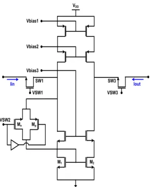
그림 6은 CMOS switch를 연결한 current memory의 schematic이다. simulation은 M2의 width 값을 고정하고 Mn의 width 값을 1~10um까지 변동함으로써 Mp의 width 값을 확인한다. 이 때 offset current가 약 0.5% 이 하일 경우 Mp의 width 값을 결정하였다. simulation 결 과, Mn과 Mp의 관계는 표 3과 같이 비례관계를 나타내 고, Mn이 2~6um일 경우에 Mn과 Mp의 width는
의 관계로 정의되고, Mn가 6~
10um일 경우에 width는 의 관계 로 정의된다.
VDD
M1
Mn Mp
Vbias1
Vbias2
Vbias3
SW1 SW3
VSW1 VSW3
VSW2
Iin Iout
M2
그림 6. CMOS switch를 연결한 current memory의 schematic Fig. 6 Schematic of current memory with CMOS switch
Mn Mp
2 12.4
3 18.4
4 24.7
5 30
6 34.7
7 37.3
8 39.58
9 41.4
10 42.9
표 3. CMOS switch (Mn, Mp)의 width관계 Table 3. The relation between width of Mn and Mp
IV. 결 론
다양한 무선통신 방식이 출현됨에 따라 통신의 지속 성과 이동성을 보장하고, 배터리 수명과 저전력 동작에 대한 연구가 활발히 진행 중이다. 따라서 저전력 동작 이 가능한 SI circuit을 이용하는 analog current-mode 신호처리가 주목되었다. 그러나 SI circuit을 구성하는 current memory는 transistor의 비선형적인 동작과 mismatch에 의해 clock-feedthrough의 문제점을 갖는 다. 본 논문에서는 current memory의 문제점인 clock- feedthrough의 해결방안으로 일반적으로 적용하고 있 는 CMOS switch의 연결을 검토하였고, current me- mory의 성능향상의 설계방안을 제안하기 위하여 CMOS switch 간의 width의 관계를 도출하였다. Sim- ulation 결과, memory MOS (M2)의 width가 20um이 고, input current와 bias current ratio (i/J)의 관계가 0.3일 때, CMOS switch의 nMOS(Mn)이 2~6um일 경 우에 Mn과 Mp의 width는 의 관 계로 정의되고, Mn가 6~10um일 경우에 width는
의 관계로 정의된다. 이 때 정의 된 MOS transistor의 관계는 memory MOS의 성능향 상을 위한 설계에 유용한 지침이 될 것으로 기대된다.
참고 문헌
[1] H. C. Yang, T. S. Fiez and D. J. Allstot,
“Current-Feedthrough Effects and Cancellation Techniques in Switched-Current Circuits”, in proc. IEEE Int. Symp. Circuits and Systems, Vol. 2, pp.3186-3188, May 1990.
[2] Terri S. Fiez and David J. Allstot, “CMOS Switched-Current Ladder Filters”, IEEE JOURNAL OF SOLID-STATE CIRCUITS, Vol. 25, No. 6, Dec.
1990.
[3] Ganesh Kumar Balachandran and Phillip E.
Allen, “Switched-Current Circuits in Digital CMOS Technology With Low Charge-Injection Errors”, IEEE JOURNAL OF SOLID-STATE CIRCUITS, Vol. 37, No. 10, Oct. 2002.
[4] Jorge M. Martins and Victor, “Harmonic Distortion in Switched-Current Audio Memory Cells”, IEEE Transactions on Circuits and System-Ⅱ: Analog and Digital Signal Processing, Vol. 46, No. 3, March 1999.
저자 소개
김성권(Seong-kweon Kim) 1996년 : 인하대학교 전자재료공과 졸업 (공학사)
2002년 : 일본 Tohoku 대학교 대학원 전자공학과 (공학석사)
2002년 : 일본 Tohoku 대학교 대학원 전자공학과 (공학박 사)
2004년 8월 ~ 현재 : 목포해양대학교 해양전자통신공학 부 교수
※관심분야 : 무선통신용 LSI 설계, 주파수분배정책 및 주파수의 효율적 사용에 관한 연구, 고주파 회로설계, 무선통신시스템