Vol. 26, No. 11 (2016)
656
Characterization of Basal Plane Dislocations in PVT-Grown SiC by Transmission Electron Microscopy
Myoungho Jeong 1 , Dong-Yeob Kim 2 , Soon-Ku Hong 2† , Jeong Yong Lee 1 , Im Gyu Yeo 3 , Tai-Hee Eun 3 and Myoung-Chuel Chun 4
1Department of Materials Science and Engineering, Korea Advanced Institute of Science and Technology (KAIST), Daejeon 34141, Republic of Korea
2Department of Materials Science and Engineering, Chungnam National University, Daejeon 34134, Republic of Korea
3Hybrid Materials Research Department, RIST, Pohang 37673, Republic of Korea
4POSCO Center, Seoul 06194, Republic of Korea
(Received October 4, 2016 : Revised October 20, 2016 : Accepted October 24, 2016)
Abstract
4H- and 6H-SiC grown by physical vapor transport method were investigated by transmission electron microscopy (TEM). From the TEM diffraction patterns observed along the [11-20] zone axis, 4H- and 6H-SiC were identified due to their additional diffraction spots, indicating atomic stacking sequences. However, identification was not possible in the [10-10] zone axis due to the absence of additional diffraction spots. Basal plane dislocations (BPDs) were investigated in the TEM specimen prepared along the [10-10] zone axis using the two-beam technique. BPDs were two Shockley partial dislocations with a stacking fault (SF) between them. Shockley partial BPDs arrayed along the [0001] growth direction were observed in the investigated 4H-SiC. This arrayed configuration of Shockley partial BPDs cannot be recognized from the plan view TEM with the [0001] zone axis. The evaluated distances between the two Shockley partial dislocations for the investigated samples were similar to the equilibrium distance, with values of several hundreds of nanometers or even values as large as over a few micrometers.Key words
silicon carbide, basal plane dislocation, Shockley partial dislocation, stacking fault, transmission electron microscope.1. Introduction
Silicon carbide(SiC) is promising material for power semiconductor devices and several companies in USA, EU, Japan, China, and Korea have developed single crystal bulk growth to provide substrates for electronic or power devices like bipolar junction transistor(BJT), Schottky Barrier Diode(SBD), and metal-oxide-semicon- ductor field-effect transistor(MOSFET). Among the bulk growth methods physical vapor transport(PVT) method is commercially beneficial method in providing substrate of large diameter as six inches and of relatively low defects densities. However, the defects such as basal plane dislo- cation(BPD), threading edge dislocation(TED), and thread- ing screw dislocation(TSD) are main obstacles for the performance of SiC-based devices, although the well-
known defect, micropipe(MP) is almost free in the state- of-the-art PVT grown SiC.
1-3)There have been researches on elimination of structural defects, however, a complete elimination of defects is unrealizable yet. 4H-SiC grown by PVT method has dislocations densities in the range of
~10
3cm
−2for BPD and threading dislocation(TD).
4)Although BPDs and TDs are the main defects in PVT- grown SiC, BPD is more important issue by two reasons:
one is the density of BPDs is generally higher than that of TDs and the other is BPDs can easily glide during the growth because BPDs are placed on the basal plane, which is the most active slip plane with close-packed atoms in hexagonal crystal system. The Burgers vectors BPDs in 4H- and 6H-SiC are mostly 1/3<11-20> in case of perfect dislocation and 1/3<10-10> in case of partial
†
Corresponding author
E-Mail : soonku@cnu.ac.kr (S.-H. Hong, Chungnam Nat'l Univ.)
© Materials Research Society of Korea, All rights reserved.
This is an Open-Access article distributed under the terms of the Creative Commons Attribution Non-Commercial License (http://creative-
commons.org/licenses/by-nc/3.0) which permits unrestricted non-commercial use, distribution, and reproduction in any medium, provided the
original work is properly cited.
dislocation. The dislocation with Burgers vector of 1/
3<10-10> is called as Shockley partial dislocation. Since the stacking fault energy of SiC is much smaller than other compound semiconductors,
5)it is expected that BPDs in 4H- and 6H-SiC are Shockley partial dislocations, which are dissociated from the perfect dislocation with formation of stacking fault(SF) between them through the following dislocation reactions, for example: 1/3[2-1-10]
→ 1/3[1-100] + 1/3[10-10].
In order to characterize BPDs and TDs transmission electron microscopy(TEM)
6,7)and synchrotron white beam x-ray topography(SWBXT)
8-11)are most powerful tools because of the ability to determine the Burgers vector of dislocations and hence can investigate detail characteristics.
However, due to the low resolution of SWBXT of about a few micrometers BPDs dissociated into two Shockley partial dislocations from the perfect dislocations could not be distinguished and be observed as single perfect dislocation. In fact, distances between two Shockley partial dislocations in 4H-SiC are about 30~70 nanometers de- pending on the SF types and energies, while those are about 150~350 nanometers.
12)Therefore, in case of two dissociated Shockley partial dislocations separated at dis- tances with the equilibrium distance or with similar to the equilibrium distance can not be distinguished by SWBXT. In case of extended SFs, in which two Shockley partial dislocations separated further by gliding of dislocations due to the applied shear stress the dis- sociated partial dislocations possibly can be observed even in the SWBXT, although there are seldom reports on observation of dissociated two Shockley partial dislo- cations. However, in case of TEM we can distinguish two Shockley partial dislocations easily regardless of whether the related SFs were extended or not.
Although TEM can observe the dissociated two Shockley partial dislocations simultaneously, there are few works in observing the dissociated Shockley partial BPDs by TEM.
12)In observing the dissociated Shockley partial BPDs, TEM observations along the [0001] zone axis is preferred in the TEM specimen prepared by plan-view with (0001) SiC wafers because the BPDs are inevitably located on the (0001) plane. However, we can observe dissociated two Shockley partial dislocations and related stacking fault planes from the orthogonal zone axis such as [10-10] zone axis.
In this work, we characterized PVT grown 4H- and 6H-SiC samples through <10-10> and <11-20> zone axes. Diffraction patterns showing the periodicity of 4H and 6H stacking sequences observed from the <11-20>
zone axis. Dissociated two Shockley partial BPDs with fringes of black and white contrast of SFs were clearly observed from the <10-10> zone axis. Furthermore, aligned BPDs with extended SFs along the <0001> growth
direction, which is impossible to recognize from the
<0001> zone axis observation, were investigated from the <10-10> zone axis.
2. Experimental
4H- and 6H-SiC bulk crystals were grown by means of PVT. The growth parameters are listed below; tempera- ture around 2,200-2,400
oC, growth pressure around 10- 40 mbar of an argon pressure. The vertical thermal gradi- ent across the SiC crystal during growth is estimated in the range of 10-15
oC/cm. The cylindrical 6H-SiC PVT ingot with a diameter of 4 inches was sliced parallel to the (10-10) plane and the 4H-SiC was sliced parallel to the (0001) plane. The sliced 4H- and 6H-SiC were pro- cessed to get mirror-like surface by polishing and chemo- mechanical polishing processes. Thin TEM specimens were prepared along the [10-10] zone axis to investigate BPDs. For the standard TEM diffraction patterns for the 4H- and 6H-SiC, cross-sectional TEM specimens along the [11-20] and the [10-10] zone axes were prepared from the other SiC wafers with (0001) plane. High- resolution TEM(HRTEM) images for the 4H- and 6H- SiC were obtained along the [11-20] zone axis. TEM specimens were prepared by mechanical polishing with a tripod polisher followed by Ar
+ion miller at 3.0 kV (695 PIPS
TMII, Gatan). TEM observations were performed by using a JEOL JEM-3010 microscope operating at 300 keV. For the Burgers vector analysis two-beam technique was applied.
3. Results and Discussion
Fig. 1 shows TEM diffraction patterns from 4H- and 6H-SiC from [11-20] and [10-10] zone axes. 4H-SiC has lattice constants of a = 0.3073 nm and c = 1.0053 nm.
13)Based on the x-ray powder diffraction data, interplanar d- spacing of the (0004) planes with diffration in 4H-SiC is 0.2513 nm.
13)As shown in Fig. 1(a) 4H-SiC shows periodic stacking sequence of 4H with additional four diffraction spots between the transmitted beam and spot for the (0004) plane, in which the first spot from the transmitted beam corresponding to the d-spacing for the lattice con- stant value of c = 1.0053 nm. Therefore, TEM diffraction pattern from the [11-20] zone axis directly reveal the atomic stacking sequence characteristics for the 4H-SiC.
In case of the 6H-SiC, which has lattice constants of a =
0.3073 nm and c = 1.508 nm,
14)interplanar d-spacing of
the (00012) planes with diffraction in 6H-SiC is 0.1256
nm.
14)In Fig. 1(c), TEM diffraction pattern obtained
from the 6H-SiC along the [11-20] zone axis shows
periodic stacking sequence of 6H with additional six
diffraction spots between the transmitted beam and spot
for the (0006) plane, in which the first spot from the transmitted beam corresponding to the d-spacing for the lattice constant value of c = 1.508 nm. On the other hand, in cases of [10-10] zone axis for both 4H- and 6H-SiC no additional diffraction spots for the atomic stacking sequence are not revealed. As shown in Fig. 1(b) and (d) only the strong spot corresponding to the (0002) plane is appearing for both 4H- and 6H-SiC. No that the TEM diffraction patterns along the [10-10] zone axis are almost identical without the additional diffraction spots, which implies that we can not identify 4H- and 6H-SiC from the TEM diffraction patterns obtained from the [10-10]
zone axis.
Fig. 2 shows HRTEM images for the 4H- and 6H-SiC.
In order to observe the atomic stacking sequence of 4H- and 6H-SiC HRTEM images should be taken from the [11-20] zone axis with additional diffraction spots. Fig.
2(a) and (b) shows HRTEM for atomic sequences of
“…ABCB...” for 4H-SiC and “…ABCACB…” for 6H- SiC, respectively. Insets in Fig. 2(a) and (b) show digital diffraction patterns obtained from the HRTEM images by fast Fourier transformation, which basically same to the patterns shown in Fig. 1(a) and (c).
Fig. 3 shows series of bright-field TEM micrographs for the dislocations observed in 6H-SiC. The TEM speci- men for Fig. 3 was prepared from the 6H-SiC wafer sliced parallel to {10-10} plane of SiC, hence the zone axis is [10-10] SiC. In the Fig. 3(a), recorded under the on-axis align to the zone axis of [10-10], it can be seen that the two dislocations(marked by arrows) are arranged side by side which expected on the same {0001} plane.
The possible position for the {0001} plane is mentioned
by dotted line. The contrast of the dislocations periodically oscillates along the line where the dislocations intersect TEM specimen surface. To figure out the characteristic Burgers vector of these dislocations, we have conducted two-beam technique investigation on them. The invisibility criteria in two-beam technique states that contrast pro- duced by a dislocation disappears when both g·b = 0 and g·(b × u) = 0 conditions are satisfied where g, b, and u are the diffraction vector, Burgers vector, and dislocation line direction vector, respectively. Fig. 3 shows the TEM images of them, bright-field TEM images taken under zone axis of [10-10](Fig. 3a), g = 0006(Fig. 3b), g = 1- 210(Fig. 3c), and g = 1-216(Fig. 3d) two-beam conditions.
Here diffraction patterns for the two-beam conditions were shown in the inset of each figure. In Fig. 3(b), re- Fig. 2. HRTEM micrographs observed along the [11-20] zone axis:
(a) 4H-SiC and (b) 6H-SiC. Insets show digital diffraction patterns obtained by fast Fourier transformation.
Fig. 3. TEM micrographs observed along the [10-10] zone axis from the 6H-SiC: a) BF image obtained with the zone axis, (b) two-beam BF image obtained with g = 0006, (c) two-beam BF image obtained with g = 1-210, (d) two-beam BF image obtained with g = 1-216, (e) magnified image of (c), and (f) magnified image of (d). Insets show corresponding diffraction patterns for each condition.
Fig. 1. TEM diffraction patterns from 4H- and 6H-SiC from [11-
20] and [10-10] zone axes: (a) 4H-SiC along the [11-20] zone axis,
(b) 4H-SiC along the [10-10] zone axis, (c) 6H-SiC along the [11-
20] zone axis, and (d) 6H-SiC along the [10-10] zone axis.
corded under g = 0006 two-beam condition, dislocations are out of contrast while they are visible in Fig. 3(c) and 3(d). This means that the dislocations have Burgers vector of 1/3[1-100] or 1/3[01-10], which is Shockley partial dislocation. The “marking” indicated by arrow in Fig. 3(a) is the intentional electron beam damage created to characterize observing area and tracking the dislo- cations in the serious of two-beam conditions, which need tilt of the TEM specimen. Fig. 3(e) and 3(f) are the magnified images of Fig. 2(c) and 2(d), respectively. It is clearly seen the black/white oscillating fringe on the partial dislocations caused by the SFs between the two Shockley partial dislocations and the SF plane.
In Fig. 3 we could observe two Shockley partial dislo- cations bounding SF. As discussed, Equilibrium distance between two Shockley partial dislocations in 6H-SiC is about 150~350 nanometers.
12)From Fig. 3 we can evaluate the distance between two Shockley partial dislocations considering the geometry. First of all, we have to address the running direction of dislocations on (0001) basal plane in Fig. 3. Due to the periodic bonding force acting across the slip plane, the energy of the dislocation core, i.e. the Peierls potential varies periodically as the dislo- cation moves.
15)Dislocations in covalently bonded materials tend to lie in the deep Peierls potential troughs, which run in low index directions.
15)Therefore, dislocations on basal plane in SiC mostly run along the <11-20> direction.
In other words, two Shockley partial dislocations in Fig.
3(a), which is projected to the [10-10] direction, runs along the <11-20> family directions on the (0001) basal plane. Here we assume the dislocations run along the [11-20] direction as shown in Fig. 4. In Fig. 4, L1 is the observed dislocation length projected to the [10-10]
direction. This value is about 310 nm in Fig. 3(a). L2 in Fig. 4 indicates observed distance between two dislo- cations. From Fig. 3(a) this is measured to about 550 nm.
Note that the distance L2 is not the real distance between the two Shockley partial dislocations because it is one on the projected image. The real distance between the two Shockley partial dislocations, D mentioned in Fig. 4, can be simply calculated from D = L2 sin 60 = 470 nm. The distance value of 470 nm determined from Fig. 3 and 4 is larger than the equilibrium distance but not so much.
Therefore, we think that two Shockley partial dislo- cations observed in Fig. 3 roughly lie in the equilibrium without significant extension.
Fig. 5 shows schematic illustration of Two Shockley partial dislocations and SF plane for the results in Fig.3.
The observed dislocation length is about 310 nm. Since the dislocation cannot terminated solely inside the material we can think the dislocation ends lie on the top and bottom surfaces of the TEM specimen. The very thin thickness of TEM specimen results in short length of the
observed dislocation of about 310 nm. This is mentioned to t in Fig. 5 as the thickness of TEM specimen. In Fig.
5 hexagonal unit cell is simply drawn on (0001) basal plane and the [11-20] direction is mentioned. In Fig. 5, D indicates the distance between the two Shockley partial dislocations similarly to Fig. 4. Two Shockley partials and SF plane are mentioned in Fig. 5. As observed and Fig. 5. Schematic illustration for the configuration of two Shockley partial BPDs and SF plane between them on (0001) basal plane.
Hexagonal unit and [11-20] direction are drawn on (0001) plane.
D indicates distance between two Shockley partial dislocations. L indicates length of Shockley partial dislocations, which is same to the thickness of thin TEM specimen, t.
Fig. 4. Schematic illustration for determination of the distance
between two Shockley partial dislocations observed in Fig. 3(a). L1
means the observed dislocation length in projected TEM image. L2
means the observed distance in the projected TEM image. D means
real distance between two Shockley partial dislocations.
as illustrated two Shockley partial dislocation and SF plane can be clearly recognized by two-beam technique from the TEM observations along the [10-10] zone axis.
Fig. 6 shows TEM micrographs from 6H-SiC, where TEM specimen is prepared along the [10-10] zone axis from the sample sliced parallel to the (0001). Fig. 6(a) is taken under the [10-10] zone axis. High density of basal plane Shockley partial dislocations, the same BPDs dis- cussed in Fig. 3, are observed. Interesting point is the BPDs are roughly arrayed along the [0001] growth direction. Fig. 6(b) show the same region to Fig. 6(a) but observed with [1-210] two-beam condition. Here we clearly see SFs bounded to each Shockley partial dislo- cations. However, in this case the SF plane spread over the whole image and the SFs are fully extended. There- fore we only one Shockley partial dislocation is imaged for each SF. The reason for such BPDs array along the [0001] growth direction is not clearly but it might be related to polymorph transition between 4H-SiC and 6H-
SiC.
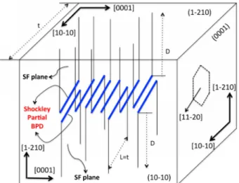
In order to provide quick reorganization of dislocation configuration schematic illustration is given in Fig. 7. In Fig. 7, t is the thickness of TEM specimen, which is same to the observed dislocation length, L. BPDs on (0001) plane are Shockley partial dislocations, which are arrayed along the [0001] growth direction. Each SF plane to each Shockley partial dislocation is drawn. SF on each Shockley partial dislocation is extended fully and only one SF is given for each SF. The D has no practical meaning here because it does not mean the equilibrium distance between two Shockley partial dislocations. We could not measure the distance D due to the limited field of view in the TEM specimen. The SFs spread over the several micrometers, which implied shear stress large enough to extended SFs implied during the growth. Here, it should be mentioned that such configuration of arrayed of Shockley partial BPDs cannot be recognized from the plan view TEM with the [0001] zone axis.
4. Conclusions
PVT grown 4H- and 6H-SiC were investigated by TEM. TEM diffraction patterns with additional diffraction spots indicating atomic stacking sequences of 4H- and 6H-SiC were observed along the [11-20] zone axis, while no additional spots were observed in the [10-10] zone axis. This means we can identify 4H- and 6H-SiC from TEM diffraction patterns observed along the [11-20] zone axis, while we cannot identify in the [10-10] zone axis.
BPDs were investigated by TEM with [10-10] zone axis.
BPDs are Shockley partial dislocations with Burgers vector of 1/3<1-100> and SFs between two Shockley partial dislocations were observable. The distances bet- ween two Shockley partial dislocations are different sample by sample in this study. The distances between two Shockley partial dislocation evacuated in 6H-SiC was about 470 nm in the investigated sample. BPDs arrayed along the [0001] growth directions were observed in 4H-SiC. The BPDs are Shockley partial dislocations and fully extended over several micrometers, which implied shear stress large enough to glide Shockley partial dislocations were applied during the growth in case of the investigated 4H-SiC sample. Here, it should be mentioned that such configuration of arrayed of Shockley partial BPDs cannot be recognized from the plan view TEM with the [0001] zone axis.
Acknowledgment
This work was supported by the research fund of Chungnam National University(Grant No. 2014-2076-01).
Fig. 7. Schematic illustration for the configuration of arrayed Shockley partial BPDs and SF planes on (0001) basal plane.
Fig. 6. TEM micrographs observed along the [10-10] zone axis from
the 4H-SiC: a) BF image obtained with the zone axis, which shows
Shockley partial BPDs arrayed along the [0001] growth direction
and (b) two-beam BF image obtained with g = 1-210, which shows
SFs on each Shockley partial dislocation.
References
1. P. Pirouz and J. W. Yang, Ultramicroscopy, 51, 189 (1993).
2. P. G. Neudeck and J. A. Powell, IEEE Electron Device Lett., 15, 63 (1994).
3. N. Iwamoto, B. C. Johnson, N. Hoshino, M. Ito, H.
Tsuchida, K. Kojima and T. Ohshima, J. Appl. Phys., 113, 143714 (2013).
4. B. Kallinger, B. Thomas and J. Friedrich, Mater. Sci.
Forum, 600-603, 143 (2007).
5. U. Lindefelt, H. Iwata, S. Öberg and P. R. Briddon, Phys.
Rev. B 67, 155204 (2003)
6. J. W. Lee, M. Skowronski, E. K. Sanchez and G. Chung, J. Cryst. Growth, 310, 4126 (2008).
7. S. Chung, V. Wheeler, R. Myers-Ward, C. R. Eddy, D. K.
Gaskill, P. Wu, Y. N. Picard and M. Skowronski, J. Appl.
Phys., 109, 094906 (2011).
8. T. Ohno, H. Yamaguchi, S. Kuroda, K. Kojima, T. Suzuki
and K. Arai, J. Cryst. Growth, 271, 1 (2004).
9. M. Skowronski, J. Q. Liu, W. M. Vetter, M. Dudley, C.
Hallin and H. Lendenmann, J. Appl. Phys., 92, 4699 (2002).
10. X. Zhang, S. Ha, Y. Hanlumnyang, C. H. Chou, V.
Rodriguez, M. Skowronski, J. J. Sumakeris, M. J. Paisley and M. J. O’Loughlin, J. Appl. Phys., 101, 053517 (2007).
11. H. Wang, F. Wu, S. Byrappa, S. Sun, B. Raghothamachar, M. Dudley, E. K. Sanchez, D. Hansen, R. Drachev, S. G.
Mueller and M. J. Loboda, Appl. Phys. Lett., 100, 172105 (2012).
12. H. Iwata, U. Lindefelt, S. Öberg and P. R. Briddon, J.
Phys.: Condens. Matter 14, 12733 (2002).
13. JCPDS card #22-1317 14. JCPDS card #29-1131
15. D. B. Holt and B. G. Yacobi, Extended Defects in Semi- conductors, p.106, Cambridge University Press, Cambridge, England (2007).
![Fig. 3. TEM micrographs observed along the [10-10] zone axis from the 6H-SiC: a) BF image obtained with the zone axis, (b) two-beam BF image obtained with g = 0006, (c) two-beam BF image obtained with g = 1-210, (d) two-beam BF image obtained with g = 1-2](https://thumb-ap.123doks.com/thumbv2/123dokinfo/5549673.470073/3.892.468.814.402.712/micrographs-observed-image-obtained-image-obtained-obtained-obtained.webp)