93 PISSN 0304-128X, EISSN 2233-9558
Zn(O
x,S
1-x) 버퍼층 적용을 통한 Cu
2ZnSnS
4태양전지 특성 향상
양기정† · 심준형 · 손대호 · 이상주 · 김영일 · 윤도영*
대구경북과학기술원 태양에너지융합연구센터 42988 대구광역시 달성군 현풍면 테크노중앙대로 333
*광운대학교 화학공학과 01897 서울특별시 노원구 광운로 20
(2016년 8월 26일 접수, 2016년 11월 8일 수정본 접수, 2016년 11월 23일 채택)
Improvement of Cu
2ZnSnS
4Solar Cell Characteristics with Zn(O
x,S
1-x) Buffer Layer
Kee-Jeong Yang†, Jun-Hyoung Sim, Dae-Ho Son, Sang-Ju Lee, Young-Ill Kim and Do-Young Yoon*
Convergence Research Center for Solar Energy, Daegu Gyeongbuk Institute of Science & Technology (DGIST), 333, Techno jungang-daero, Hyeonpung-myeon, Dalseong-gun, Daegu, 42988, Korea
*Department of Chemical Engineering, Kwangwoon University, 20, Gwangun-ro, Nowon-gu, Seoul, 01897, Korea (Received 26 August 2016; Received in revised form 8 November 2016; accepted 23 November 2016)
요 약
본 실험에서는 Cu2ZnSnS4(CZTS) 태양전지의 흡수층 상부에 다양한 조성을 갖는 Zn(Ox,S1-x) 버퍼층을 적용하여 특 성 변화를 살펴보았다. Zn(O0.76,S0.24), Zn(O0.56, S0.44), Zn(O0.33,S0.67) 그리고 Zn(O0.17,S0.83)의 4가지 단일막의 경우, 전자- 정공의 재결합 억제에 유리한 밴드갭 구조를 나타내는 Zn(O0.76,S0.24) 버퍼층을 소자에 적용했다. Zn(O0.76,S0.24) 버퍼 층을 소자에 적용 시, 흡수층으로부터 S가 버퍼층으로 확산되어 소자 내에서의 버퍼층은 Zn(O0.7,S0.3)의 조성을 나타 냈다. CdS 버퍼층의 EV보다 낮은 에너지 준위를 갖는 Zn(O0.7,S0.3) 버퍼층은 전자-정공 재결합을 효과적으로 억제하기 때문에 CZTS 태양전지의 JSC와 VOC특성을 향상시켰다. 이를 통해 CdS 버퍼층이 적용된 CZTS 태양전지의 효율인 2.75%가 Zn(O0.7,S0.3) 버퍼층 적용을 통해 4.86%로 향상되었다.
Abstract – This experiment investigated characteristic changes in a Cu2ZnSnS4(CZTS) solar cell by applying a Zn (Ox,S1-x) butter layer with various compositions on the upper side of the absorber layer. Among the four single layers such as Zn(O0.76,S0.24), Zn(O0.56, S0.44), Zn(O0.33,S0.67), and Zn(O0.17,S0.83), the Zn(O0.76,S0.24) buffer layer was applied to the device due to its bandgap structure for suppressing electron-hole recombination. In the application of the Zn(O0.76,S0.24) buffer layer to the device, the buffer layer in the device showed the composition of Zn(O0.7,S0.3) because S diffused into the buffer layer from the absorber layer. The Zn(O0.7,S0.3) buffer layer, having a lower energy level (EV) than a CdS buffer layer, improved the JSC and VOC characteristics of the CZTS solar cell because the Zn(O0.7,S0.3) buffer layer effectively suppressed electron-hole recombination. A substitution of the CdS buffer layer by the Zn(O0.7,S0.3) buf- fer layer improved the efficiency of the CZTS solar cell from 2.75% to 4.86%.
Key words: Solar cell, CZTS, Buffer layer, Open circuit voltage, Current density
1. 서 론
기후 변화에 대응하기 위해서는 태양광 발전(solar photovoltaics), 태양열 발전(solar thermal) 등과 같은 신재생 에너지의 개발이 필 요하다[1]. 이 중에서 태양광 발전은 무한한 태양광을 전기로 전환
할 수 있는 장점이 있으나, 실생활에 활용하기 위해서는 낮은 가격과 높은 에너지 변환 효율(power conversion efficiencies, PCE)을 통 한 높은 에너지 밀도의 확보가 필요하다. 저가의 태양광 발전 구현을 위해 많은 무기물 물질이 제안되었으며[2], 이 중에서 Cu2ZnSnS4 (CZTS) 흡수층과 관련된 물질을 사용하는 태양광 발전 기술은 지 구상에 널리 존재하는 물질을 사용하고, 1.0~1.5 eV의 유용한 밴드 갭 에너지 범위와, 104 cm-1이상의 흡수 계수 특성을 나타내기 때 문에 많은 주목을 받고 있다[3-5]. 그러나 CdTe 박막 태양전지가 21.5%[6], CIGS 박막 태양전지가 22.6%[7]의 광전변환 효율을 나 타내는 것에 비해 CZTSSe 박막 태양전지는 12.6%[8]의 광전변환
†To whom correspondence should be addressed.
E-mail: [email protected]
‡이 논문은 광운대학교 한 춘 교수님의 정년을 기념하여 투고되었습니다.
This is an Open-Access article distributed under the terms of the Creative Com- mons Attribution Non-Commercial License (http://creativecommons.org/licenses/by- nc/3.0) which permits unrestricted non-commercial use, distribution, and reproduc- tion in any medium, provided the original work is properly cited.
효율을 보이고 있어 실생활에 적용하기 위해서는 효율의 향상이 필 요하다. CZTS 박막 태양전지의 효율 향상을 위해서는 전류와 전압 손실을 최소화하는 것이 중요하다. 이를 위해서 흡수층 내의 결정 성 향상[9,10], 이차상 생성의 억제[10-16], 결함 생성 제어[10,15- 19], Na 양의 조절[20,21], 그리고 흡수층 내의 밴드갭 변화 조절 [16,22-25] 등이 필요하다. 또한 현재 박막 태양전지에 적용되고 있는 CdS 버퍼층의 경우, 카드뮴(Cd)의 적용에 의한 환경 오염 문제 해 결과, 흡수층과의 최적의 에너지 밴드 구조를 구현해야 한다[5,26].
또한 흡수층과 버퍼층 계면에서의 전자-정공 재결합 현상은 태양전 지 특성 저하의 또 다른 원인이 될 수 있다[20,21]. 이러한 문제를 해결하기 위해 Cd가 포함되지 않은 버퍼층에 관한 연구 결과가 보 고되고 있으며, 이 중에서 Zn 관련 물질에 대한 버퍼층이 많은 관 심을 받고 있다[27-35]. Zn(Ox,S1-x) 버퍼층의 경우, 산소(O)와 황 (S)의 비율에 따라서 흡수층과 다양한 에너지 밴드 구조를 나타낼 수 있다[36-38]. 흡수층과 버퍼층의 가장 최적의 에너지 밴드 구조는 전도대(conduction band, EC)에서 적절한 에너지 차이를 나타내면서 전자의 이동을 원활히 해야 한다. 그리고 가전자대(valence band, EV)에 서는 흡수층의 가전자대보다 낮은 버퍼층의 에너지 준위를 나타내 면서 정공의 이동에 대한 장벽 역할을 통해 흡수층-버퍼층 계면에서 전자-정공의 재결합을 억제할 수 있어야 한다[30,31,34,35-37]. 본 연구 에서는 원자층 증착법을 이용하여 Zn(Ox,S1-x) 버퍼층을 형성하고, CZTS 박막 태양전지의 특성을 향상 시킬 수 있는 방법을 제시한다.
2. 실험방법
CZTS 박막 태양전지는 알루미늄(Al) 전면전극 / Al 도핑된 ZnO 투명층 / ZnO / 버퍼층 / CZTS 흡수층 / 몰리브데늄(Mo) 후면전극 / 소다라임 유리기판(sodalime glass, SLG)의 구조로 제작되었다.
SLG 위에 Mo 후면 전극을 형성 뒤, 스퍼터링 공정을 이용하여 Mo 후면 전극 상부에 ZnS (140 nm, 200 W RF power)-SnS (120 nm, 200W RF power)-Cu (70 nm, 150 W DC power)의 순서로 CZTS 전구체(precursor)를 증착했다. 증착된 전구체는 상압의 570oC 열 처리 조건에서 황(S) 소스를 적용하여 쿼츠 로(quartz furnace)에서 열처리 공정을 통해 약 600 nm 두께의 흡수층이 형성되었다. 흡수 층 형성 후 CdS와 Zn(Ox,S1-x)의 두 가지 버퍼층을 각각 적용했다.
CdS 버퍼층은 화학적 용액 성장법(Chemical Bath, Deposition, CBD)을 이용해 60 nm 두께로 형성되었다. Zn(Ox,S1-x)는 원자층 증착법 (Atomic Layer Deposition, ALD)을 이용해 증착했으며, Zn(Ox,S1-x) 중 O와 S의 비율을 조절했다. 이 후 스퍼터링 방법으로 50 nm 두께의 ZnO층과 300 nm 두께의 Al이 도핑된 ZnO 투명 전극층을 증착했다.
CZTS 박막 태양전지의 특성 평가는 주사투과현미경-에너지분산형 분광 분석법(Scanning Transmission Electron Microscopy-Energy Dispersive Spectrometry, STEM-EDS), 솔라 시뮬레이터(Solar Simulator), 그리고 외부양자효율(External Quantum Efficiency, EQE)을 통해 서 수행했다. 박막 내 물질 조성 및 분포를 확인하기 위해 사용한 STEM-EDS은 Bruker 사의 모델명 QUANTAX-200를 사용했다.
CZTS 박막 태양전지의 전기적 특성 및 효율을 측정하기 위해 사용한 솔라 시뮬레이터는 air mass 1.5 global (AM 1.5 G) 스펙트럼의 100 mW/cm2 (1sun) 광조사 조건에서 Newport 사의 모델명 94022A를 사용했다. EQE는 McScience 사의 SR 830 DSP lock-in amplifier 시스템을 사용했다.
3. 결과 및 고찰
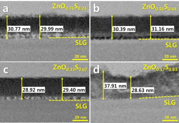
Fig. 1은 유리 기판 위에 각각 다른 ALD 공정 조건으로 증착한 Zn(Ox,S1-x) 박막의 TEM 이미지와 EDS scan을 통한 박막의 조성
Fig. 1. Cross-sectional TEM images of (Zn(Ox,S1-x) layers with various deposition conditions. (a) Zn(O0.76,S0.24), (b) Zn(O0.56,S0.44) (c) Zn (O0.33,S0.67) and (d) Zn(O0.17,S0.83). The elemental ratio in TEM images were measured using EDS area scan.
비를 나타내고 있다. ALD 증착 공정 중에 Zn(Ox,S1-x) 박막의 Zn 소스로는 diethylzinc (DEZn), S 소스로는 황화수소(H2S), 산소(O) 소스로는 H2O를 적용했다. ALD 증착 조건에 따라서 Fig. 1과 같 이 4가지의 O:S 비율을 나타내는 Zn(Ox,S1-x) 박막을 확인했다. Fig.
1a와 b의 경우, Zn(Ox,S1-x) 박막 내에 O의 비율이 높고, Fig. 1c와 d의 경우, Zn(Ox,S1-x) 박막 내에 S의 비율이 높다. Zn(Ox,S1-x)는 O와 S의 비율에 따라서 다른 에너지 밴드 특징을 나타낸다. 따라서 흡수 층인 CZTS와의 에너지 밴드 접합 구조도 다르게 나타나게 된다.
Fig. 2는 CdS와 Zn(Ox,S1-x) 버퍼층과 CZTS 흡수층과의 에너지 밴 드 구조를 도식화한 것이다[38-41]. CdS 버퍼층의 EC는 CZTS 흡 수층의 EC보다 0.09 eV 낮게 위치하고 있고, CdS 버퍼층의 EV는 CZTS 흡수층의 EV보다 1.01 eV 낮게 위치하고 있다. Zn(Ox,S1-x)는 O와 S의 비율에 따라서 EC는 CZTS 흡수층의 EC보다 0.97 eV 높은 경우부터 0.34 eV 낮은 경우까지 위치하고, EV는 CZTS 흡수층의 EV보다 1.29 eV 부터 2.19 eV 범위까지 낮게 위치하고 있다. 버퍼 층의 경우, 에너지 밴드갭이 클수록 전자-정공의 재결합 억제 효과 가 커진다. Fig. 2로부터, Fig. 1c와 d의 경우는 에너지 밴드갭이 가 장 크지만, EC는 CZTS 흡수층의 EC보다 0.34 eV 높게 위치하고 있어, 흡수층에서 생성된 전자의 이동에 방해가 될 수 있다. 그러나 큰 에너지 밴드갭을 보이는 Fig. 1a의 Zn(O0.76,S0.24) 버퍼층의 경우,
EC가 CZTS 흡수층의 EC보다 0.17 eV 정도 낮게 위치하고 있어 비 교적 차이가 적어서 전자의 이동을 가능하게 하고, EV는 CZTS 흡 수층의 EV보다 1.64 eV 이상 낮게 위치하고 있어 정공의 이동을 억 제해서 전자-정공의 재결합을 억제할 수 있을 것이다. 따라서 Zn(O0.76,S0.24) 버퍼층을 적용해서 CZTS 박막 태양전지를 제작했다.
Fig. 3은 버퍼층으로 CdS가 적용된 CZTS 박막 태양전지의 STEM 이미지, EDS mapping 이미지와 EDS line scan 결과이다.
Fig. 3a와 같이 Mo 후면 전극은 흡수층의 열처리 공정 중에 S와 반 응하여 흡수층 계면에서 MoSx가 형성되었다. 또한 CZTS 흡수층과 ZnO/AZO 사이에 CdS 버퍼층이 형성되어 있음을 알 수 있다. Fig.
3b, c와 d는 Fig. 3a의 버퍼층 부근에 대한 EDS mapping 이미지이 다. Fig. 3b로부터 CdS 버퍼층 중 Cd의 분포를 알 수 있다. Cd는 흡수층과 ZnO/AZO 층 사이에 불균일하게 분포하고 있음을 알 수 있다. 따라서 CdS 버퍼층 역시 불균일하게 분포하고 있을 것이다.
P-type의 특성을 보이는 흡수층의 표면은 버퍼층에 의해서 도핑되어 n-type이 형성될 경우, 전자-정공의 분리가 원활이 일어날 수 있어 단락전류밀도(short circuit current density, JSC) 특성이 향상될 수 있다[39,40]. 그러나 Fig. 3b와 같이 CdS 버퍼층이 불균일하게 형 성되어 있을 경우, 흡수층의 표면 도핑 효과 역시 불균일하게 되어 Fig. 2. The band diagram between CdS, ZnS, Zn(O0.3,S0.7), Zn(O0.5,S0.5),
Zn(O0.7,S0.3), Zn(O0.9,S0.1) ZnO, and CZTS.
Fig. 3. Compositional distributions determined using EDS measure- ments. From cross-sectional STEM images, localized composi- tions were measured and elemental distributions near the CdS buffer layer were mapped. Elemental variations across the vertical directions in STEM images were measured using EDS line scans.
JSC특성 향상 효과는 감소될 수 있다. Fig. 3e는 Fig. 3a의 화살표 부분에 대해 EDS line scan을 통해서 CdS 버퍼층 부근에서의 조성 분포를 나타내고 있다. 형성된 CdS 버퍼층의 두께는 약 60nm이며, Cd와 S의 비율이 1:1로 형성되어 있음을 알 수 있다. CZTS 흡수층 에서의 조성비는 Cu/(Zn+Sn)=0.87, Zn/Sn=1.2로 Cu-poor, Zn-rich 의 일반적인 조성비를 나타내고 있다.
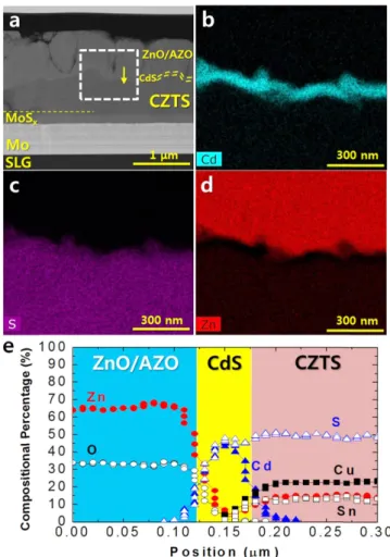
Fig. 4는 버퍼층으로 Zn(Ox,S1-x)가 적용된 CZTS 박막 태양전지 의 STEM 이미지, EDS mapping 이미지와 EDS line scan 결과이 다. Fig. 3a와 같이 Fig. 4a에서도 Mo 후면 전극과 흡수층 계면에서 MoSx가 형성되었음을 알 수 있다. 또한 CZTS 흡수층과 ZnO/AZO 사이에 Zn(Ox,S1-x) 버퍼층이 형성되어 있음을 알 수 있다. Fig. 4b, c와 d는 Fig. 4a의 일부분에 대한 EDS mapping 이미지이다. Fig. 3의 CdS 버퍼층과 비교해보면, Fig. 4c와 d의 EDS mapping 이미지로 부터 Zn(Ox,S1-x) 버퍼층이 비교적 균일하게 형성되었음을 알 수 있다.
Fig. 4e는 Fig. 4a의 화살표 부분에 대해 EDS line scan을 통해서 Zn(Ox,S1-x) 버퍼층 부근에서의 조성 분포를 나타내고 있다. 형성된 Zn(Ox,S1-x) 버퍼층의 두께는 약 30 nm이며, O와 S의 비율이 0.7:0.3으 로, Zn(O0.7,S0.3)의 버퍼층이 형성되었다. Fig. 1a의 Zn(O0.76,S0.24) 버퍼층 증착 조건으로 CZTS 흡수층에 적용했을 경우, S가 CZTS 흡수층으로부터 Zn(Ox,S1-x) 버퍼층으로 일부 확산되어 S의 조성이 다소 증가했다. 따라서 Zn(Ox,S1-x) 단일막 증착 조건과 소자 적용 시에 O와 S의 비율이 달라질 수 있기 때문에, 소자 적용 시에는 S의 확산을 고려해야 한다. CZTS 흡수층에서의 조성비는 Cu/(Zn+Sn)
=0.88, Zn/Sn=1.2로 Cu-poor, Zn-rich의 일반적인 조성비를 나타내 고 있다.
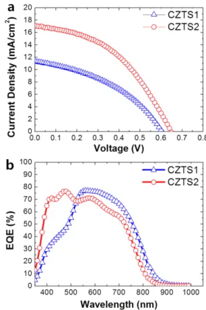
Table 1은 CdS 버퍼층과 Zn(O0.7,S0.3)의 버퍼층이 적용된 소자의 특성을 나타내고 있다. 그리고 Fig. 5a는 전류-전압 특성 그래프이 며, Fig. 5b는 파장에 따른 CZTS 박막 태양전지의 외부양자효율 결과를 나타내고 있다. Zn(O0.7,S0.3)의 버퍼층이 적용된 CZTS2 박 막 태양전지는CdS 버퍼층이 적용된 CZTS1 박막 태양전지보다 모 두 향상된 특성을 보이고 있다. JSC의 경우, CZTS1에서는 11.3 mA/cm2인 반면, CZTS2는 17.0 mA/cm2으로 향상되었다. 이는 Fig. 2에서 설명한 바와 같이, CdS 버퍼층보다 에너지 밴드갭이 큰 Zn(O0.7,S0.3) 버퍼층의 경우, EC는 서로 비슷하지만, Zn(O0.7,S0.3)
Fig. 4. Compositional distributions determined using EDS measure- ments. From cross-sectional STEM images, localized com- positions were measured and elemental distributions near the Zn(O0.7,S0.3) buffer layer were mapped. Elemental vari- ations across the vertical directions in STEM images were measured using EDS line scans.
Fig. 5. CZTS solar cell characteristics: (a) current density-voltage characteristics of CZTS solar cells, and (b) EQE at a bias of 0 V.
Table 1. List of CZTS solar cell parameters
Sample Buffer layer PCE (%) VOC (V) JSC (mA/cm2) FF (%)
CZTS1 CdS 2.75 0.604 11.30 40.37
CZTS2 Zn(O0.7,S0.3) 4.86 0.647 17.00 44.22
버퍼층의 EV가 CdS 버퍼층의 EV보다 낮은 에너지 준위를 갖기 때 문에 정공의 이동 억제 효과가 상대적으로 더 크고, 따라서 전자-정 공의 재결합이 어려워 JSC가 향상된 것이다. 또한 Zn(O0.7,S0.3) 버퍼 층의 밴드갭은 2.97 eV로, CdS의 밴드갭 2.42 eV보다 크기 때문에 단파장 영역에서의 광흡수율이 CdS보다 더 크다. 따라서 Fig. 5b의 EQE 그래프에서, Zn(O0.7,S0.3) 버퍼층이 적용된 CZTS2가 500 nm 이하의 영역에서 높은 EQE 값을 나타내게 된다. 큰 흡수층-버퍼층 계면에서의 전자-정공 재결합 억제는 VOC가 향상되는 효과가 있으며, 균일하게 형성된 Zn(O0.7,S0.3) 버퍼층은 CZTS 박막 태양전지의 저 항값을 낮춰 충진율(Fill Factor, FF)이 향상되었다.
4. 결 론
박막 태양전지에 널리 적용되는 CdS 버퍼층은 Cd의 환경 오염 문제와 에너지 밴드갭이 작아 흡수층-버퍼층 계면에서 전자-정공 재결합을 효과적으로 억제하지 못하는 단점이 있다. 본 연구에서는 CdS 버퍼층보다 에너지 밴드갭이 크고, 흡수층-버퍼층 계면에서 전 자-정공 재결합을 억제할 수 있는 Zn(O0.7,S0.3) 버퍼층을 적용했다.
CdS 버퍼층의 EV보다 낮은 에너지 준위를 갖는 Zn(O0.7,S0.3) 버퍼 층은 전자-정공 재결합 억제 효과의 향상으로 CZTS 박막 태양전지의 JSC와 VOC특성을 향상시켰다. 또한 CdS 버퍼층보다 균일하게 형 성될 수 있는 ALD 공정으로 증착된 Zn(O0.7,S0.3) 버퍼층은 박막 태양전지의 저항을 향상시켜 FF를 향상시켰다. 이를 통해서 CZTS 박막 태양전지의 효율은 약 1.8배 향상되었다. 이러한 Zn(Ox,S1-x) 버퍼층의 적용은 향후 박막 태양전지의 효율을 향상시키는 연구에 적용될 수 있다.
감 사
본 연구는 미래창조과학부에서 지원하는 DGIST 일반사업에 의해 수행되었습니다(16-DB-05).
Notation PCE : Power conversion efficiency EC : Conduction band
EV : Valence band Eg : Bandgap energy
JSC : Short circuit current density VOC : Open circuit voltage FF : Fill factor
References
1. Hallegatte, S., Bangalore, M., Bonzanigo, L., Fay, M., Kane, T., Narloch, U., Rozenberg, J., Treguer, D. and Vogt-Schilb, A.,
“Shock Waves: Managing the Impacts of Climate Change on Poverty,” World Bank Group, USA(2016).
2. Wadia, C., Alivisatos, A. P. and Kammen, D. M., “Materials Availability Expands the Opportunity for Large-Scale Photovol- taics Deployment,” Environ. Sci. Technol., 43, 2072-2077(2009).
3. Jean, J., Brown, P. R., Jaffe, R. L., Buonassisi, T. and Bulovic,
V., “Pathways for Solar Photovoltaics,” Energy Environ. Sci., 8, 1200-1219(2015).
4. Ramasamy, K., Malik, M. A. and O’Brien, P., “Routes to Copper Zinc Tin Sulfide Cu2ZnSnS4 a Potential Material for Solar Cells,” Chem. Commun., 48, 5703-5714(2012).
5. Winkler, M. T., Wang, W., Gunawan, O., Hovel, H. J., Todorov, T. K. and Mitzi, D. B., “Optical Designs that Improve the Effi- ciency of Cu2ZnSn(S,Se)4 Solar Cells,” Energy Environ. Sci., 7, 1029-1036(2014).
6. Green, M. A., Emery, K., Hishikawa, Y., Warta, W. and Dunlop, E. D., “Solar Cell Efficiency Tables (version 46),” Prog. Photovolt:
Res. Appl., 23, 805-812(2015).
7. Jackson, P., Wuerz, R., Hariskos, D., Lotter, E., Witte, W. and Powalla, M., “Effects of Heavy Alkali Elements in Cu(In,Ga)Se2 Solar Cells with Efficiencies up to 22.6%,” Phys. Status Solidi RRL, 10(8), 583-586(2016).
8. Wang, W., Winkler, M. T., Gunawan, O., Gokmen, T., Todorov, T. K., Zhu, Y. and Mitzi, D. B., “Device Characteristics of CZTSSe Thin-Film Solar Cells with 12.6% Efficiency,” Adv. Energ. Mater., 4, 1301465(2014).
9. Son, D., Kim, D., Park, S., Yang, K., Nam, D., Cheong, H. and Kang, J., “Growth and Device Characteristics of CZTSSe Thin-Film Solar Cells with 8.03% Efficiency,” Chem. Mater., 27, 5180-5188 (2015).
10. Yang, K., Sim, J., Son, D., Kim, D., Kim, G. Y., Jo, W., Song, S., Kim, J., Nam, D., Cheong, H. and Kang, J., “Effects of the Com- positional Ratio Distribution with Sulfurization Temperatures in the Absorber Layer on the Defect and Surface Electrical Char- acteristics of Cu2ZnSnS4 Solar Cells,” Prog. Photovolt: Res. Appl., 23, 1771-1784(2015).
11. Fairbrother, A., Fontané, X., Izquierdo-Roca, V., Placidi, M., Sylla, D., Espindola-Rodriguez, M., López-Mariño, S., Pulgarín, F. A., Vigil-Galán, O., Pérez-Rodríguez, A. and Saucedo, E., “Secondary Phase Formation in Zn-rich Cu2ZnSnSe4-based Solar Cells Annealed in Low Pressure and Temperature Conditions,” Prog. Photovolt:
Res. Appl., 22, 479-487(2014).
12. Vigil-Galán, O., Espíndola-Rodríguez, M., Courel, M., Fontané, X., Sylla, D., Izquierdo-Roca, V., Fairbrother, A., Saucedo, E.
and Pérez-Rodríguez, A., “Secondary Phases Dependence on Composition Ratio in Sprayed Cu2ZnSnS4 Thin Films and Its Impact on the High Power Conversion Efficiency,” Sol. Energ.
Mater. Sol. Cells, 117, 246-250(2013).
13. Colombara, D., Robert, E. V. C., Crossay, A., Taylor, A., Guen- nou, M., Arasimowicz, M., Malaquias, J. C. B., Djemour, R. and Dale, P. J., “Quantification of Surface ZnSe in Cu2ZnSnSe4-Based Solar Cells by Analysis of the Spectral Response,” Sol. Energ.
Mater. Sol. Cells, 123, 220-227(2014).
14. Wätjen, J. T., Engman, J., Edoff, M. and Platzer-Björkman, C.,
“Direct Evidence of Current Blocking by ZnSe in Cu2ZnSnSe4 Solar Cells,” Appl. Phys. Lett., 100, 173510(2012).
15. Kumar, M., Dubey, A., Adhikari, N., Venkatesan, S. and Qiao, Q., “Strategic Review of Secondary Phases, Defects and Defect- complexes in Kesterite CZTS-Se Solar Cells,” Energy Environ.
Sci., 8, 3134-3159(2015).
16. Huang, T. J., Yin, X., Qi, G. and Gong, H., “CZTS-based Mate- rials and Interfaces and Their Effects on the Performance of Thin Film Solar Cells,” Phys. Stat. Sol., 8(9), 735-762(2014).
of Lattice Defects in the Kesterite Cu2ZnSnS4 and Cu2ZnSnSe4 Earth-Abundant Solar Cell Absorbers,” Adv. Mater., 25, 1522- 1539(2013).
18. Chen, S., Yang, J., Gong, X. G., Walsh, A. and Wei, S., “Intrinsic Point Defects and Complexes in the Quaternary Kesterite Semi- conductor Cu2ZnSnS4,” Phys. Rev. B, 81, 245204(2010).
19. Yin, W. J., Wu, Y., Wei, S. H., Noufi, R., Al-Jassim, M. M. and Yan, Y., “Engineering Grain Boundaries in Cu2ZnSnSe4 for Better Cell Performance: A First-Principle Study,” Adv. Energ. Mater., 4, 1300712(2014).
20. Yang, K., Sim, J., Jeon, B., Son, D., Kim, D., Sung, S., Hwang, D., Song, S., Khadka, D. B., Kim, J. and Kang, J., “Effects of Na and MoS2 on Cu2ZnSnS4 Thin-film Solar Cell,” Prog. Photovolt:
Res. Appl., 23, 862-873(2015).
21. Yang, K., Sim, J., Son, D., Kim, D. and Kang, J., “Two Different Effects of Na on Cu2ZnSnS4 Thin-film Solar Cells,” Curr. Appl.
Phys., 15, 1512-1515(2015).
22. Woo, K., Kim, Y., Yang, W., Kim, K., Kim, I., Oh, Y., Kim, J. Y.
and Moon, J., “Band-gap-graded Cu2ZnSn(S1-x,Sex)4 Solar Cells Fabricated by an Ethanol-based, Particulate Precursor Ink Route,”
Sci. Rep., 3, 3069(2013).
23. Wei, H., Ye, Z., Li, M., Su, Y., Yang, Z. and Zhang, Y., “Tunable Band Gap Cu2ZnSnS4xSe4(1-x) Nanocrystals: Experimental and First-principles Calculations,” CrystEngComm, 13, 2222-2226(2011).
24. Malerba, C., Biccari, F., Ricardo, C. L. A., Valentini, M., Chierchia, R., Müller, M., Santoni, A., Esposito, E., Mangiapane, P., Scardi, P. and Mittiga, A., “CZTS Stoichiometry Effects on the Band Gap Energy,” J. Alloys Compd, 582, 528-534(2014).
25. Yang, K., Son, D., Sung, S., Sim, J., Kim, Y., Park, S., Jeon, D., Kim, J., Hwang, D., Jeon, C., Nam, D., Cheong, H., Kang, J. and Kim, D., “A Band-gap-graded CZTSSe Solar Cell with 12.3%
Efficiency,” J. Mater. Chem. A, 4, 10151-10158(2016).
26. Bär, M., Schubert, B.A., Marsen, B., Wilks, R. G., Pookpanratana, S., Blum, M., Krause, S., Unold, T., Yang, W., Weinhardt, L., Heske, C. and Schock, H. W., “Cliff-like Conduction Band Offset and KCN-induced Recombination Barrier Enhancement at the CdS/
Cu2ZnSnS4 Thin-film Solar Cell Heterojunction,” APL, 99, 222105 (2011).
27. Platzer-Björkman, C., Törndahl, T., Abou-Ras, D., Malmström, J., Kessler, J. and Stolt, L., “(Zn(Ox,S1-x) Buffer Layers by Atomic Layer Deposition in Cu(In,Ga)Se2 Based Thin Film Solar Cells:
Band Alignment and Sulfur Gradient,” J. Appl. Phys., 100, 044506 (2006).
28. Larina, L., Shin, D., Kim, J. H. and Ahn, B. T., “Alignment of Energy Levels at the ZnS/Cu(In,Ga)Se2 Interface,” Energy Envi- ron. Sci., 4, 3487-3493(2011).
Torndahl, T. and Platzer-Bjorkman, C., “Zn(O, S) Buffer Layers and Thickness Variations of CdS Buffer for Cu2ZnSnS4 Solar Cells,” IEEE J. Photovolt., 4(1), 465-469(2014).
30. Kobayashi, T., Kumazaw, T., Kao, Z. J. L. and Nakada, T.,
“Cu(In,Ga)Se2 Thin Film Solar Cells with a Combined ALD- (Zn(Ox,S1-x) Buffer and MOCVD-ZnO:B Window Layers,” Sol.
Energy Mat. Sol. Cells, 119, 129-133(2013).
31. Barkhouse, D. A. R., Haight, R., Sakai, N., Hiroi, H., Sugimoto, H. and Mitzi, D. B., “Cd-free Buffer Layer Materials on Cu2ZnSn (SxSe1-x)4: Band Alignments with ZnO, ZnS, and In2S3,” APL, 100, 193904(2012).
32. Klenk, R., Steigert, A., Rissom, T., Greiner, D., Kaufmann, C.
A., Unold, T. and Lux-Steiner, M. C., “Junction Formation by (Zn(Ox,S1-x) Sputtering Yields CIGSe Based Cells with Efficiencies Exceeding 18%,” Prog. Photovolt: Res. Appl., 22, 161-165(2014).
33. Hultqvist, A., Platzer-Bjorkman, C., Coronel, E. and Edoff, M.,
“Experimental Investigation of Cu(In1-x,Gax)Se2/Zn(O1-z,Sz) Solar Cell Performance,” Sol. Energy Mat. Sol. Cells, 95, 497-503(2011).
34. Shin, D. H., Kim, J. H., Shin, Y. M., Yoon, K. H., Al-Ammar, E.
A. and Ahn, B. T., “Improvement of the Cell Performance in the ZnS/Cu(In,Ga)Se2 Solar Cells by the Sputter Deposition of a Bilayer ZnO: Al Film,” Prog. Photovolt: Res. Appl., 21, 217-225 (2013).
35. Huang, S., Luo, W. and Zou, Z., “Band Positions and Photoelec- trochemical Properties of Cu2ZnSnS4 Thin Films by the Ultrasonic Spray Pyrolysis Method,” J. Phys. D: Appl. Phys., 46, 235108 (2013).
36. Schmid, D., Ruckh, M. and Schock, H. W., “A Comprehensive Characterization of the Interfaces in Mo/CIS/CdS/ZnO Solar Cell Structures,” Sol. Energy Mat. Sol. Cells, 41/42, 281-294(1996).
37. Minemoto, T., Hashimoto, Y., Satoh, T., Negami, T., Takakura, H. and Hamakawa, Y., “Cu(In,Ga)Se2 Solar Cells with Controlled Conduction Band Offset of Window/Cu(In,Ga)Se2 Layers,” J.
Appl. Phys., 89(12), 8327-8330(2001).
38. Persson, C., “Strong Valence-band Offset Bowing of ZnO1-xSx Enhances p-Type Nitrogen Doping of ZnO-like Alloys,” Phys.
Rev. Lett. PRL, 97, 146403(2006).
39. Chen, S., Walsh, A., Yang, J. H., Gong, X. G., Sun, L., Yang, P.
X., Chu, J. H. and Wei, S. H., “Compositional Dependence of Structural and Electronic Properties of Cu2ZnSn(S,Se)4 Alloys for Thin Film Solar Cells,” Phys. Rev. B, 83, 125201(2011).
40. Zhang, S. B., Wei, S. H. and Zunger, A., “A Phenomenological Model for Systematization and Prediction of Doping Limits in II-VI and I-III-VI2 Compounds,” J. Appl. Phys., 83(6), 3192-3196 (1998).