제 2 회 첨단 사이언스 교육 허브 개발(EDISON) 나노물리 경진대회
Simulation of nano MOS gate tunneling current with SiO 2 /Er 2 O 3 double-layer gate dielectrics
Seok Man Hong, Hyeon Jun Ha, Young Sun Moon
School of Electrical Engineering, Korea University, Seoul 136-701, South Korea.
e-mail:[email protected], [email protected], [email protected]
ABSTRACT
Nano MOS with Er2O3/SiO2 double-layer gate dielectrics was demonstrated by EDISON Nanophysics software. Double-layer structure decreases the gate leakage current in two orders compared with SiO2 single-layer gate dielectric.
INTRODUCTION
The continuous reduction of the SiO2 layer thickness for advanced metal-oxide-semiconductor field-effect transistor (MOSFET), the gate leakage current becomes unacceptably large due to the quantum-tunneling limit of 1.5-2.5 nm. To resolve this issue, high-k materials such as Al2O3, ZrO2, HfO2, La2O3, Y2O3, and Gd2O3, are widely studied for future MOSFET gate dielectric. The high-k gate dielectrics must be processed at high- temperature thermal treatment to achieve a chemical stability for standard complementary metal-oxide-semiconductor (CMOS) process.
However, the thermal treatments degrade the quality of the dielectric films generating silicide and silicates at the interface. These resulted in recrystallization of the dielectric film, which eventually induces a higher leakage current and lower channel mobility [1]. Recently, some researchers have reported that Er2O3 thin film was deposited on Si substrate shows a promising gate dielectric material because of high dielectric constant (k = 14) and excellent electrical properties.
Moreover, Er2O3 are also interesting that it has large conduction band offset on Si (~3.5 eV) due to its large band gaps (~5.4 eV). These properties effectively suppress the different type of leakages which are made by Schottky emission of electrons into the band states or donor-type oxygen vacancies [2].
In a nano MOS gate stack with a high-k dielectric material, the structure of a double-layer (high-k layer and SiO2 layer) gate dielectric is
known as improving the channel carrier mobility [4]. These advantages are originated from improving instability with Si and reduction of high trap density of high-k material. Moreover, this structure relieves electrical stress between gate dielectric, leading to increase device reliability.
Nevertheless, so far there are no simulation reports on double-layer gate dielectric (Er2O3 layer and SiO2 layer) for nano MOS device. Hence, to precisely design the double layer structure with Er2O3 high-k film, we optimized the double-layer gate dielectric structure with Er2O3 and SiO2 layer by EDISON Nanophysics software.
RESULTS AND DISCUSSION
In this study, different gate stacks are used to simulate the electron transport in nano MOS device. The EDISON Nanophysics software for nano MOS device is capable of simulating quantum-mechanical electron tunnelling based on the non-equilibrium Green’s function (NEGF) formalism [3]. We compare reference structure composed of a single-layer and double-layer gate dielectric stacks. In EDISON Nanophysics software, we are able to modify some parameters such as thickness, dielectric constants, effective mass, and conduction band offset. Firstly, the simulation of the nano MOS with single SiO2 (2.5 nm) gate dielectric and with Er2O3 (8.897 nm) gate dielectric were performed. In this simulation, SiO2
and Er2O3 gate dielectrics are with the same equivalent oxide thickness (EOT) of 2.5 nm. The EOT formula is
9 , .
2 3
k high k
high SiO k high
eq t
t
−
−
− =
=
ε ε
ε
(1)Where ε is the dielectric constant and t is the material thickness. The parameters for SiO2 gate dielectric are relative permittivity of 10, effective mass of 0.38 and conduction band offset of 4.3 eV.
54 252
제 2 회 첨단 사이언스 교육 허브 개발(EDISON) 나노물리 경진대회
And the parameters for Er2O3 gate dielectric are relative permittivity of 14, effective mass of 0.25 and conduction band offset of 3.5 eV. The physical parameters we used in simulation are given in Table 1 and the physical thicknesses of nano MOS gate stacks and EOT are arranged in Table 2. Fig.
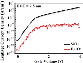
1 shows the gate leakage current densities versus gate voltage (VG) of SiO2 and Er2O3 single-layer gate dielectrics. We observed that the gate leakage current is effectively reduced in Er2O3 single-layer gate dielectrics. This result is because the physical thickness of Er2O3 gate dielectric is much higher than that of SiO2 gate dielectric. In EOT = 2.5 nm device, the thickness of SiO2 gate dielectric is 2.5 nm and the thickness of Er2O3 gate dielectric is 8.897 nm. It is proven that the physically thicker gate dielectric suppress the tunnelling current.
Next, the capacitance characteristics of SiO2 and Er2O3 single-layer gate dielectric are shown in Fig.
2. It is clearly found that the capacitance of Er2O3
single-layer gate dielectric maintains the same capacitance as SiO2 single-layer gate dielectric.
Although Er2O3 gate dielectric is thicker than SiO2
gate dielectric, higher relative permittivity of Er2O3 keeps the capacitance holding. This suggests that Er2O3 is superior gate dielectric material for nano MOS device.
After the improvement of nano MOS device performances by using single-layer high-k dielectric, double-layer gate dielectrics with Er2O3
and SiO2 layer are used to simulate the nano MOS device. The double-layer structures are always considered to have the same EOT thickness of 2.5 nm. Two structures are considered: a double-layer
gate stack composed of an interfacial SiO2 (1 nm) layer and a high-k Er2O3 (5.384 nm) layer, and an interfacial SiO2 (0.5 nm) layer and a high-k Er2O3
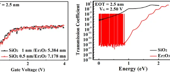
(7.178 nm) layer. The physical thicknesses of double-layer gate stacks are 6.384 nm and 7.678 nm, respectively. Fig. 3 shows a comparison of the gate leakage current densities through the gate stack versus gate voltage in the different structures.
Considering the leakage current density of single- layer SiO2 dielectric structure, the leakage current densities of two structures decrease effectively by suppressing vertical tunneling. Among two structures, the gate leakage current density of SiO2
(1 nm) + Er2O3 (5.384 nm) gate stack is slightly higher near the gate voltage of 1V. Such behaviour is due to different thickness of two structures. Gate current increases when SiO2 layer thickness increases from 0.5 nm to 1 nm because the total gate stack thickness is reduced from 7.678 nm to
Fig. 1. The gate current density-voltage characteristics of nano MOS with single- layer gate dielectrics (SiO2 and Er2O3).
Fig. 2. The capacitance characteristics of nano MOS with single-layer gate dielectrics (SiO2 and Er2O3).
TABLE 1. Physical parameters of different gate dielectrics for nano MOS simulation.
Gate dielectric
Physical parameter EG
(eV) ε/ε0 m*/m0 ΔEC
SiO2 9.0 3.9 0.22 4.3
Er2O3 5.4 14 0.25 3.5
TABLE 2. Physical thicknesses and EOT of nano MOS gate stacks simulation.
Gate stacks Physical thickness (nm) SiO2 Er2O3 EOT
SiO2 2.5 - 2.5
Er2O3 - 14 2.5
SiO2/Er2O3 1 5.384 2.5
SiO2/Er2O3 0.5 7.178 2.5
55 253
제 2 회 첨단 사이언스 교육 허브 개발(EDISON) 나노물리 경진대회
6.384 nm. However, it is still interesting that the gate leakage current of double-layer gate stack is the same as single-layer Er2O3 gate dielectric even though the physical thickness is thinner than single-layer Er2O3 layer. We believe that small variation of Er2O3 thickness cannot be taken into account for simulation due to high relative dielectric constant of Er2O3 dielectric layer.
The capacitances of double-layer gate stacks are shown in Fig. 4. In this case, two double-layer structures have the same capacitance because we designed the structure based on the same EOT = 2.5 nm. Even though there are no significant enhancements of nano MOS device performance by using double-layer gate dielectrics with SiO2
and Er2O3, the simulation of gate leakage current and capacitance are meaningful results. This is because many papers refer that Er2O3 layer
deposited on Si produce thin SiO2 interfacial layer between Er2O3 and Si during thermal treatment [5].
For further understanding of single and double- layer gate stacks, the tunnelling transmission coefficient calculated using the EDISON Nanophysics software. The transmission coefficient describes the behaviour of wave incident on a barrier. It is often used to explain the probability of a particle tunnelling through a barrier. Fig. 5 shows the tunnelling transmission coefficient of single-layer gate dielectrics. Note that Er2O3 gate stack shows the randomness distribution of the transmission coefficient from 0 eV to 0.8 eV might be error during simulation, and numerous peaks stem from NEGF formalism. We can observe on the Fig. 5 that the single-layer SiO2
and Er2O3 gate dielectric leads to significant differences between the two gate dielectrics.
Single-layer Er2O3 gate dielectric shows small
Fig. 5. The gate current density-voltage characteristics of nano MOS with two dielectric layer.
Fig. 6. The capacitance characteristics of nano MOS with two dielectric layer.
Fig. 3. The gate current density-voltage characteristics of nano MOS with tow dielectric layer (SiO2 and Er2O3/SiO2).
Fig. 4. The capacitance characteristics of nano MOS with tow dielectric layer (SiO2 and Er2O3/SiO2).
56 254
제 2 회 첨단 사이언스 교육 허브 개발(EDISON) 나노물리 경진대회
transmission coefficient causing low gate leakage current. However, physically thinner gate dielectric (SiO2) is vulnerable to electron tunneling.
Since the tunneling coefficient approaches to 1 above 1.6 eV, we predict that the electrons which get energy above 1.6 eV easily tunnel through gate dielectric, resulting in high gate leakage current. In addition, the transmission coefficients of double- layer gate stacks are shown in Fig. 6. From the transmission coefficient of single-layer gate dielectric result, the physically thick double-layer with SiO2 (0.5 nm) + Er2O3 (7.178 nm) would show lower transmission coefficient than SiO2 (1 nm) + Er2O3 (5.384 nm). However, we observe that the transmission are enhanced at SiO2 (0.5 nm) + Er2O3 (7.178 nm) gate stack. This result might be due to very thin SiO2 layer. Electrons can tunnel through very thin SiO2 layer (0.5 nm) because a direct tunneling mechanism is predominant in this very thin layer. Therefore, a strong potential discontinuity, induced by a
conduction band offset between SiO2 and Er2O3, creates a potential well, leading to discrete energy levels and high transmission coefficient [6].
Finally, the local density of states (LDOS) has been computed by EDISON nanophysics software.
The quantum-mechanical effect is clear in Fig. 7.
In these figures, reddish area represents high- density of states and blush area displays low- density of states. The fringes near the contacts illustrate the existence of interferences between incident and reflected wave function on the barrier [6]. Fig. 7(a) shows that fringes are less reddish than the other figure, representing reflected wave function is small portion of incident wave function.
Since Fig. 7(b), (c), and (d) show large bluish area, they contribute to low level gate leakage current density.
CONCLUSION
In summary, we simulated the double-layer gate dielectric by EDISON Nanophysics software to optimize the precise design of the double-layer structure with Er2O3 and SiO2. Among the proposed double-layer structures, SiO2 (1 nm) + Er2O3 (5.384 nm) is the most effective gate dielectric structure considering physical thickness, gate leakage current density, capacitance and the transmission coefficient.
REFERENCES
[3] O. Baumgartner, M. Karner, and H. Kosina, SISPAD, pp.
353 (2008)
[1] T.-M. Pan, C.-L. Chen, W.W. Yeh, and S.-J. Hou, App.
Phys. Lett., 89 222912 (2006)
[2] V. Mikhelashvili and G. Eisenstein, J. Appl. Phys., 95 613 (2004)
[4] N. Ikarashi, K. Watanabe, K. Masuzaki, and T. Nakagawa, App. Phys. Lett., 88 101912 (2006)
[5] H.S. Kamineni, V.K. Kamineni, R.L. Moore II, S. Gallies, A.C. Deibold, M. Huang, and A.E. Kaloyeros, J. Appl.
Phys., 111 013104 (2012)
[6] M. Moreau, D. Munteanu, and J.-L Autran, Jpn. J. App.
Phys., 48 111409 (2009) Fig. 7. Computed LDOS in nano MOS with respect to Position
(nm), Energy (eV) with (a) single-layer SiO2 (2.5 nm) (b) single-layer Er2O3 (8.897 nm) (c) double-layer SiO2 (1 nm) + Er2O3 (5.384 nm) and (d) double-layer SiO2 (0.5 nm) + Er2O3 (7.178 nm).
57 255