http://dx.doi.org/ 10.5515/KJKIEES.2012.23.5.559 ISSN 1226-3133 (Print)
. 서 론
(Radar Detector: RD)
2011 ( ) (No. 2010-0013273).
(Department of Electronic Information and Communication Engineering, Hongik University) Manuscript received October 13, 2011 ; February 1, 2012 ; February 20, 2012. (ID No. 20111013-124)
Corresponding Author : Jeong-Hae Lee (e-mail : [email protected])
X, K
X, K-Band Patch Array Antenna Having One Port Feeding for Radar Detector
주현모 박병철 계영철 이정해
Hyun-Mo Joo Byung-Chul Park Young-Chul Kay Jeong-Hae Lee 요 약
X (10.525 GHz) 1×2 K (24.15
GHz) 3×6 . X K
. , stub
. T-junction
, .
open, short stub . stub
,
. X 6.47 dBi, K 13.07 dBi
.
Abstract
In this paper, the X(1×2, 10.525 GHz) and K(3×6, 24.15 GHz) bands patch array antenna having single feed line for radar detector applications is proposed. The left side of the proposed array antenna is X band array antenna and the right is K band array antenna. Two array antennas with two stubs located in the front of antennas are fed through one transmission line. If the array antennas which have the different resonance frequency are fed by one transmission line using general T-junction, it interferes each other and the array antenna lost its character. Therefore, to prevent these interferences, two stubs using open and short property of stub are designed. First of all, the performances of array antenna weren't changed when each array antennas were connected with the stub and in the end, it is found out that it was the same when the two array antennas were combined and feed through the one transmission line. The measured gain at X band is 6.47 dBi and measured gain at K band is 13.07 dBi. The experimental results agree well with the simulated ones.
Key words : Patch, Array Antenna, Single Feed, Stub, Radar Detector
. , , , ,
RD ,
[1]
.
, X (10.525 GHz), K (24.15 GHz), Ka (33.4 GHz 36 GHz)
[2].
[3]
. 3D
GPS
.
.
, .
X, K, Ka ,
. 3
.
X, K .
.
X K
, K X
[4] [7]
.
배열 안테나 설계 .
1
. X K
,
그림 1 .
Fig. 1 . Inset feed single patch antenna.
표 1 .
Table 1. Parameters of patch antenna.
W
[mm]
L
[mm]
n
[mm]
b
[mm]
X-band 9.9 7.8 2.8 0.4
K-band 4.3 3.3 0.8 0.45
1 .
[8]
. (1) .
±
(1)
(2)
・
(3)
,
.
(1) (3) .
±
(4)
(4)
.
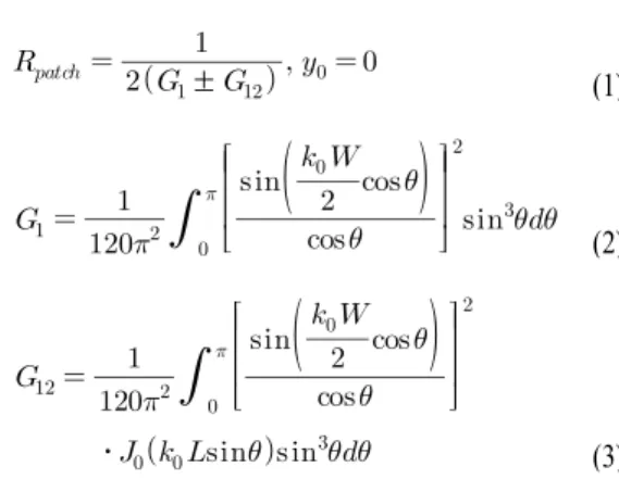
X(1×2) , K(3×6)
. X
200 Ω , K 300 Ω
. 2 X
K .
. K
1/ 4 . X
200 Ω
100 Ω .
50 Ω stub
. Stub , stub
, .
3 3×6 K .
1/ 4
(a) 1×2 X
(a) 1×2 X band array anteena
(b) 3×6 K
(b) 3×6 K band array antenna
그림 2. X, K
Fig. 2. The structure of the proposed X, K band array antenna.
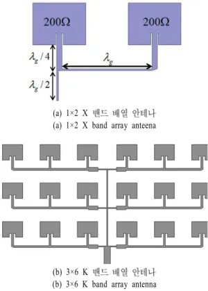
그림 3 . 1×3 K
Fig. 3. 1×3 K band array antenna.
(a)
(b)
(c)
그림 4. (a) S-parameter, (b) E-plane , (c) H-plane
Fig. 4. (a) S-parameter, (b) E-plane radiation pattern,
(c) H-plane radiation pattern.
300 Ω ,
,
,
,
(5)
[9].
(5)
(5)
,
,
,
152 , 101 , 45 , 300 Ω Ω Ω Ω .
. HFSS X, K
.
4 X 10.51 GHz
250 MHz(2.4 %)
broadside 9.83 dBi .
5 K 24.13 GHz
490 MHz(2 %) broad-
side 17.5 dBi .
. Stub 설계
stub .
SRR
[4] [7]
.
. Stub
. Stub 6 X, K
. X stub K
4 , stub
4 .
K .
short K
4 , X
open
[9]. stub
X K
.
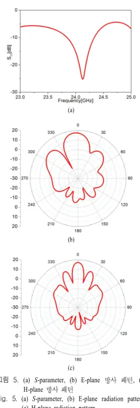
7 X stub
. Stub
(a)
(b)
(c)
그림 5. (a) S-parameter, (b) E-plane , (c) H-plane
Fig. 5 . (a) S-parameter, (b) E-plane radiation pattern, (c) H-plane radiation pattern.
,
.
(a) Stub X
(a) X band array antenna with stub
(b) Stub K
(b) K band array antenna with stub
그림 6. Stub X, K
Fig. 6. X, K band array antenna with stub.
그림 7. stub
Fig. 7. The structure and electrical property of the pro- posed stub.
.
X, K 50 Ω
100 Ω stub
.
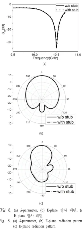
시뮬레이션 및 측정 결과 .
X, K stub
. 8 X (a)
(a)
(b)
(c)
그림 8. (a) S-parameter, (b) E-plane , (c) H-plane
Fig. 8. (a) S-parameter, (b) E-plane radiation pattern, (c) H-plane radiation pattern.
, (b) E-plane , (c) H-plane . Stub
. 9 K
E-plane, H-plane . X
stub ,
(a)
(b)
(c)
그림 9. (a) S-parameter, (b) E-plane , (c) H-plane
Fig. 9. (a) S-parameter, (b) E-plane radiation pattern, (c) H-plane radiation pattern.
(24.15 GHz)
θ=0° 17.5 dBi, 17.4
dBi .
8 9 stub
. ,
stub X, K
(a) X(10.525 GHz) (b) K(24.15 GHz)
그림 10. X .
Fig. 10. Electric field distribution at X band array an- tenna.
(a) Stub (a) Without stub
(b) Stub (b) With stub
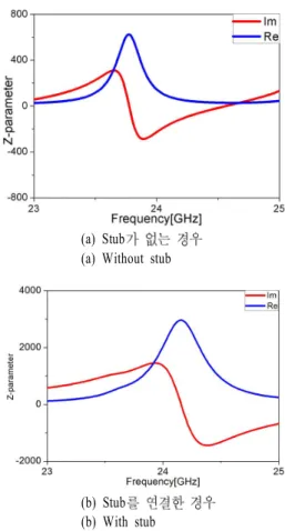
그림 11 . K (24.15 GHz) Z-parameter Fig. 11. Z-parameter at K band(24.15 GHz).
.
10 X (10.525 GHz)
, K (24.15
GHz) stub . Stub
stub K (24.15
GHz) Z-parameter . 11(b)
K 3,000 Ω .
stub K open
, K X
. Stub 11(b)
, stub K
. K
z-parameter
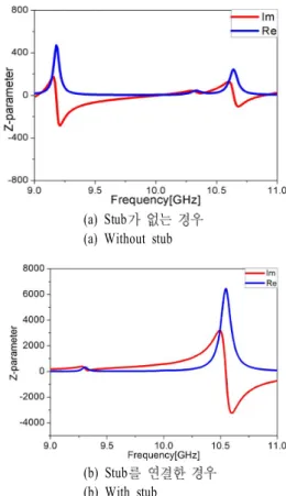
12 13 .
12 K 10.525 GHz
24.15 GHz . K
, X stub .
X z-parameter 13 .
13 10.52 GHz
6,500 Ω . K
stub X open X
. stub
2 3 .
2 3 stub
.
.
(a) K(24.15 GHz) (b) X(10.525 GHz)
그림 12 . K .
Fig. 12. Electric field distribution at K band array an- tenna.
(a) Stub (a) Without stub
(b) Stub (b) With stub
그림 13. X (10.525 GHz) Z-parameter Fig. 13. Z-parameter at X band(10.525 GHz).
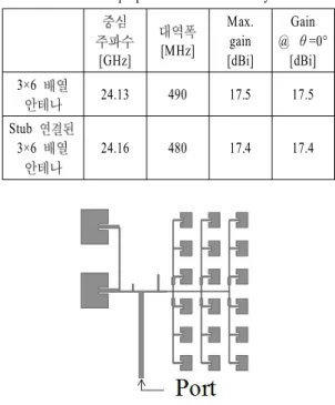
표 2 . X
Table 2. Antenna properties of X-band array antenna.
[GHz] [MHz]
Max.
gain [dBi]
Gain
@ θ=0°
[dBi]
1×2 10.51 250 9.84 9.83
Stub
1×2 10.51 250 9.56 9.55
stub X, K
14 .
X, K
15 .
15(a) X K
표 3 . K
Table 3. Antenna properties of K-band array antenna.
[GHz] [MHz]
Max.
gain [dBi]
Gain
@ θ=0°
[dBi]
3×6 24.13 490 17.5 17.5
Stub
3×6 24.16 480 17.4 17.4
그림 14.
Fig. 14 . The structure of proposed array ant.
(a) (b)
그림 15. (a) X , (b) K
Fig. 15. (a) X band electric field distribution, (b) K band electric field distribution.
, 15(b) K
X
. 16
. 3×6 K
, .
16(b) .
(a) (b)
(c)
그림 16. (a) , (b)
, (c) jig
Fig. 16. (a) Fabricated array antenna, (b) Simulation structure of fabricated array antenna, (c) Test jig.
16(a) 16(b) .
3.2 , 0.635 mm Ta-
conic TLC ,
k-connector . ,
16(c) test jig .
Test jig 150 mm×110 mm×20 mm ,
1 kg , K .
Test jig ground
X, K θ =0° 2 dBi
, 3 dB X 8° K
6° . 17 X
, E-plane, H-plane .
. ,
17 (b), (c) 10.525
GHz ,
. θ=0°
6.86 dBi , 6.47 dBi .
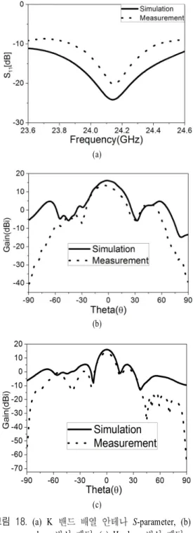
18 K , E-plane,
(a)
(b)
(c)
그림 17 . (a) X S-parameter, (b) E
plane , (c) H plane
Fig. 17. (a) S-parameter of X band array antenna, (b) E plane radiation pattern, (c) H plane radia- tion pattern.
H-plane .
. X S
11. θ=0°
7.14 dBi , 6.47 dBi . K
S
11,
(a)
(b)
(c)
그림 18 . (a) K S-parameter, (b) E
plane , (c) H plane
Fig. 18 . (a) S-parameter of K band array antenna, (b) E plane radiation pattern, (c) H plane radia- tion pattern.
10 dB ,
. θ=0° 15.65 dBi
, 13.07 dBi . ,
15.83 dBi 13.7 dBi
. 2 dBi
. test jig
, align
. , K HP-
BW 10°
.
. 결 론
X, K . 2
stub open, short
, stub
2
. X
, K
. X(10.525 GHz),
K(24.15 GHz) ,
, 2 .
참 고 문 헌