http://dx.doi.org/10.5369/JSST.2015.24.4.252 pISSN 1225-5475/eISSN 2093-7563
다중 이미지 센서의 신호처리를 위한 8-bit Single Slope ADC 설계
이종철1·이상훈1·김진태1·박재률2·신장규1·최평1,+
Design of 8-bit Single Slope ADC for Signal Processing of Multiple Image Sensors
Jong-Cheol Lee1, Sang-Hoon Lee1, Jin-Tae Kim1, Jae-Roul Park2, Jang-Kyoo Shin1, and Pyung Choi1,+
Abstract
This paper proposes a single slope A/D converter (SSADC) that is possible to process the signal of the ultraviolet, visible and infrared rays with a single chip. And the proposed SSADC is a type of single channel ADC. In the conventional SSADC, it is possible to process the only one signal with a kind of the sensor because the speed of the operating frequency and the slope of ramp signal generated by the ramp generator are fixed. In order to improve the disadvantages, a ramp generator which has variable slope in ramp function is designed and 3x1 MUX(multiplexer) is adopted so that we can change the speed of the operating frequency and the slope of ramp signal. Therefore, the multiple signal processing of the wanted sensors can be possible. The designed circuit is layout by the 0.35-µm CMOS 2-poly 4-metal technology process and is checked through DRC and LVS tools.
Keywords: Single slope A/D converter, Ultraviolet rays, Visible lights, Infrared rays, Image sensors
1. 서 론
최근 세계 반도체 공정 기술의 발전에 따라 단일 칩 시스 템(system on chip : SoC) 기술이 여러 분야에서 사용되고 있다. 그러므로 기존의 다양한 개별 칩들이 SoC화 되면서 시 스템의 소형화, 고성능화, 저전력화와 같은 성능 향상을 위한 연구가 활발히 진행되고 있다[1,2]. 특히 자외선(ultraviolet rays : UV), 가시광선(visible lights : VIS), 적외선(infrared rays : IR)센서와 같은 이미지 센서의 신호처리를 위해서는 A/D 변환기(analog to digital converter : ADC)가 반드시 필요하 다[3-9].
본 논문에서는 파장대가 다른 자외선, 가시광선, 적외선 세 가 지 이미지 센서를 하나의 ADC로 통합 신호처리가 가능한 8-
bit Single Slope A/D 변환기(SSADC)를 설계하였다. 그리고 제 안하는 SSADC는 0.35 μm CMOS 2P4M(2-poly 4-metal) 공정 규칙에 맞추어 레이아웃을 하였고, DRC(design rule check), LVS(layout versus schematic) tool을 이용하여 설계한 회로와 레 이아웃의 결과를 비교 검증하였다.
2. Single Slope A/D변환기 설계
2.1 일반적인 Single Slope A/D변환기
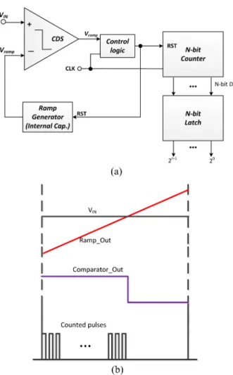
일반적인 SSADC는 Fig. 1(a)와 같이 램프 발생기(ramp generator), CDS(correlated double sampling), 제어 로직(control logic), 카운터(counter), 래치(latch)로 구성되어 있다. SSADC의 동작 원리는 Fig. 1(b)처럼 입력 신호(V in ) 와 램프 신호(V ramp ) 가 CDS에 의해 비교되어 입력 신호가 램프 신호보다 크면 high(1), 작으면 low(0) 값이 출력된다. 이 때 low(0) 값이 나오기 직전 까지 카운트된 클락 수를 n-bit에 맞는 디지털 출력으로 나타내 고 래치를 이용하여 그 값을 저장함으로써 입력 신호의 크기를 알 수 있다. 그러나 이 구조는 동작 주파수와 내부 커패시터 (capacitor) 에 의한 램프 신호가 고정된 기울기를 가지게 되어 다 른 ADC보다 동작속도가 느리면서, 하나의 특정 신호처리만 가 능하다. 또한 내부 커패시터로 인해 SSADC의 면적이 커지게 되는 단점이 있다[10-12].
1경북대학교 전자공학부(School of Electrical Engineering, Kyungpook National Unversity)
80 Daehak-ro, Buk-gu, Daegu 702-701, Korea
2경북IT융합산업기술원(Gyungbuk Institute of IT Convergence Industry Technology)
Gyeongsan-si, Gyeongsangbuk-do, Korea
+Corresponding author: [email protected] (Received : Jul 14, 2015, Accepted : Jul.28, 2015)
This is an Open Access article distributed under the terms of the Creative Commons Attribution Non-Commercial License(http://creativecommons.org/
licenses/bync/3.0) which permits unrestricted non-commercial use, distribution, and reproduction in any medium, provided the original work is properly cited.
2.2 제안하는 Single Slope A/D변환기
2.2.1 제안하는 Single Slope A/D변환기 구조
제안하는 SSADC는 Fig. 2에서 보는 바와 같이 3x1 MUX,
클락 분주기(clock divider), 램프발생기, 비교기, 8-bit 업 카운 터, 8-bit 래치로 구성되어 있다. 클락 분주기는 메인 클락을 이 용하여 필요한 3개의 서브 클락으로 변환한다. CLK_SW로 신 호처리에 필요한 서브 클락을 선택하여 SSADC를 setting 한 다. Cap_SW로 선택된 외부 커패시터에 의해 램프 신호가 발 생하게 된다. 램프 신호의 크기와 Vin_SW로 선택된 입력신호 를 비교하여 비교기의 출력 값이 low(0)가 감지될 때까지 카운 트된 클락 수를 8-bit에 맞게 디지털 신호로 출력한다.
출력된 디지털 신호의 LSB(least significant bit)의 크기는 수식 (1)을 이용하여 표현할 수 있다. 제안하는 8-bit SSADC 의 최대 전압(V max ) 이 3.3[V]이면 V LSB 는 약 12.89[mV]가 된 다. 수식 (2)는 출력된 디지털 값을 아날로그 값으로 변환하기 위한 식으로, 2진수의 디지털 값을 10진수 값으로 변경한 후 LSB의 크기를 곱하게 되면 아날로그 입력 신호의 크기를 구 할 수 있다.
(1)
(2)
2.2.2 클락 분주기와 3x1 MUX를 이용한 입력 신호 및 동 작 주파수 선택
제안하는 SSADC에서는 자외선, 가시광선, 적외선 센서의 신 호처리를 위해 하나의 메인 클락(Main_CLK)이 아닌 세 개의 클락이 필요하기 때문에 클락 분주기를 사용한다. 클락 분주기 는 Fig. 3과 같이 D 플립플롭(D F/F)을 이용하여 클락 주기가 두 배씩 증가하도록 설계하였다.
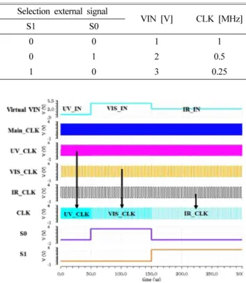
MUX 는 선택 신호를 이용하여 다수의 입력 데이터 중 사용 자가 원하는 데이터만 출력하는 선택용 전송기이다. 제안하는 SSADC 에서는 입력 센서 신호 선택용, 서브 클락 선택용, 외 부 커패시터 선택용으로 3x1 MUX를 사용하였다[13]. 외부 선택 신호(external selection signal) ‘S0’, ‘S1’을 이용하여 자 외선, 가시광선, 적외선 센서의 신호 처리에 필요한 사양 선택 을 Table 1에서 보여주고 있다. 선택 신호 ‘S0= low(0), S1=
low(0)’ 일 때 자외선 입력 신호(UV_IN), 서브 클락(UV_CLK), V
LSBV
max2
N---
=
V
out{ ( n _bit D
out)
10} V ×
LSBn 1= N
∑
=
Fig. 1. (a) Structure and (b) Operation principle of the conventional single slope ADC.
Fig. 2. Structure of the proposed single slope ADC.
Fig. 3. Structure of the proposed CLK divider.
그리고 자외선용 커패시터(Cap_UV)가 선택되고, ‘S0=high(1), S1=low(0)’ 일 때 가시광선 입력 신호(VIS_IN), 서브 클락 (VIS_CLK), 그리고 가시광선용 커패시터(Cap_VIS)가 선택되 며, ‘S0=low(0), S1=high (1)’ 일 때 적외선 입력 신호(IR_IN), 서브 클락(IR_CLK), 적외선용 커패시터(Cap_IR)가 선택 되 도록 설계하였다.
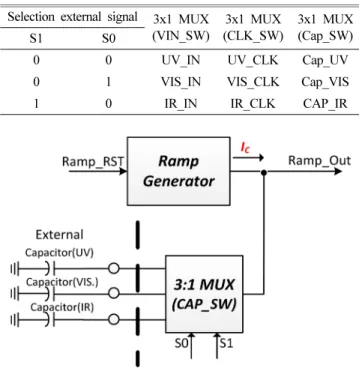
2.2.3 램프 발생기 설계
제안하는 SSADC에서 가장 중요한 역할을 담당하는 부분 인 램프 발생기는 고정 전류 값과 가변 커패시터를 이용하여 원하는 기울기의 램프 신호를 발생시키는 부분이다[14,15]. 램 프 발생기에 사용되는 커패시터를 내부에서 레이아웃 할 경우 칩 면적이 커지고 고정된 기울기의 램프 신호만 생성 되는 단 점이 있다. 이를 해결하고자 Fig. 4와 같이 커패시터를 회로 외부에 연결하여 칩 면적을 크게 줄이고 각 센서의 신호 처리 에 적합한 단일 기울기를 생성할 수 있도록 설계하였다.
램프 발생기에서 출력되는 램프 신호의 기울기를 결정하는 외부 커패시터의 용량은 수식 (3), (4), (5)를 이용하여 구할 수 있다. Ramp_Out(V out ) 의 범위는 0~V supply 이고 V out (0) 은 리셋 신 호에 의해 초기화 된 출력 값이므로 0[V]이다. I C 는 램프 발생 기 내부의 전류 미러에 의해 안정적으로 공급되는 전류이므로 고정된 값을 갖고, 변수 t는 선택된 서브 클락의 주기(T CLK ) 와 2 N (N 은 bit 수)의 곱으로 나타낼 수 있다. 따라서 제안하는 SSADC 에서 커패시터의 용량은 T CLK 과 N에 의해 변화한다.
(3)
(4)
(5)
메인 클락 주파수를 2[MHz]인 신호를 인가 하였을 때, Table.
2 는 램프 발생기 출력 신호의 기울기에 직접적인 영향을 주는 외부 커패시터의 용량 값을 보여주고 있다. 제안하는 램프 발생 기의 I c 는 약 858[nA], 자외선의 서브 클락 주파수 주기(T CLK ) 는 1[μs], 8 bit 디지털 출력이므로 N=8, V out(max) =V supply =3.3[V], V out (0) 은 초기 값이므로 0[V]이다. 주어진 변수 값을 이용하여 Cap_UV 을 계산할 경우 약 65p[F]이다.
2.2.4 동기식 8-bit Up Counter 설계
제안하는 SSADC에서 사용되는 동기식 8-bit up counter는 Fig. 5 와 같이 T플립플롭과 AND게이트를 이용하여 설계하였다.
Fig. 2 의 counter(a)는 램프 발생기, counter(b) 블록의 동기화를 목적으로, 리셋 신호를 생성하기 위해 필요한 블록이다. 서브 클 락에 의해 counter(a)가 구동되며, 출력 값이 최대치인 11111111 일 때 8x1 AND 게이트가 동작이 되어 리셋 신호를 생성한다.
counter(b) 는 비교기의 출력 신호가 0되는 시점까지 서브 클락 에 의해 동작된다. 비교기의 출력이 0가 되면 그 때까지 카운트 된 클락 수를 세어 8 bit의 병렬 디지털 값으로 변환시키고, 리 셋 신호가 인가되기 전까지 그 값을 유지한다.
I
cC dV
out--- dt
=
V
outI
cC ---- t d
∫ I
cC ----t V +
out( ) 0
= =
C I
c⋅ t V
out– V
out( ) 0 ---
t T= CLK⋅2N
= Table 1. Selection of VIN, CLK and CAP using external selection
signal
Selection external signal 3x1 MUX (VIN_SW)
3x1 MUX (CLK_SW)
3x1 MUX (Cap_SW)
S1 S0
0 0 UV_IN UV_CLK Cap_UV
0 1 VIS_IN VIS_CLK Cap_VIS
1 0 IR_IN IR_CLK CAP_IR
Fig. 4. Structure of the proposed ramp generator.
Table 2. Selected external capacitor and capacitor values for the pro- posed ramp generator
Selection external signal
External CAP Value[pF]
S1 S0
0 0 Cap_UV 65
0 1 Cap_VIS. 130
1 0 Cap_IR 260
Fig. 5. Synchronous 8-bit up counter using T flip flop.
3. 시뮬레이션 및 레이아웃
3.1 클락 분주기, CLK_SW, VIN_SW 검증
제안하는 SSADC에 메인 클락 주파수를 2[MHz]인 신호를 인 가 하고 가상 입력 신호에 자외선은 1[V], 가시광선은 3[V], 적 외선은 2[V]를 인가하였다. Fig. 6은 시뮬레이션 결과를 보여준 다. 클락 분주기에 의해 UV_CLK=1[MHz], VIS_CLK=0.5[MHz], IR_CLK=0.25[MHz] 로 변화된다. CLK_SW로 자외선, 가시광선, 적외선 신호처리에 필요한 서브 클락이 선택되고, VIN_SW에 의해 UV_IN, VIS_IN, IR_IN이 선택된다. Table 3은 시뮬레이 션에 대한 결과 값을 나타내었다.
3.2 램프 발생기 검증
Table 2 에 주어진 외부 커패시터의 값을 SSADC에 연결하고 시뮬레이션 한 결과를 Fig. 7에서 보여주고 있다. Cap_UV=65[pF], Cap_VIS=130[pF], Cap_IR=260[pF] 중 CAP_ SW에 의해 한 개 의 커패시터가 선정되어 구현하고자 하는 램프 신호를 발생하 게 된다. 만약 외부 선택 신호 S0/S1=0/0 일 경우, 65[pF]이 연 결되어 UV 신호처리용 램프 신호가 출력된다. 서브 클락 주기 (T CLK ), N=8, 커패시터 용량을 이용하여 예상되는 기울기와 실 제 시뮬레이션 결과의 기울기를 Table 4에 나타내었다.
3.3 동기식 8-bit Up Counter 검증
Counter(a)에 1[MHz] 서브 클락이 인가 되었을 경우 counter 의 출력과 8x1 AND 게이트에 의해 리셋 신호가 발생되는 시 뮬레이션 결과를 Fig. 8에서 나타내었다. 그리고 counter(b)의 검 증을 위해, 가상의 신호=1[V]를 인가하여 비교기의 출력이 0이 되는 시점 후 최종 값이 유지 되는 것을 Fig. 9에서 보여주고 있다.
Table 3. Result values of selected VIN and CLK Selection external signal
VIN [V] CLK [MHz]
S1 S0
0 0 1 1
0 1 2 0.5
1 0 3 0.25
Fig. 6. Simulation results of the clock divider, CLK_SW and VIN_SW block.
Fig. 7. Simulation results of the proposed ramp generator
Table 4. Expected and simulation result slopes for proposed the ramp generator
Selection external signal Expected slope [V/ms]
Simulation result slope [V/ms]
S1 S0
0 0 12.89 12.75
0 1 6.45 6.42
1 0 3.22 3.17
Fig. 8. Simulation results of the proposed 8-bit Up Counter(a) block
3.4 제안하는 single slope A/D변환기 시뮬레이션 및 레이 아웃
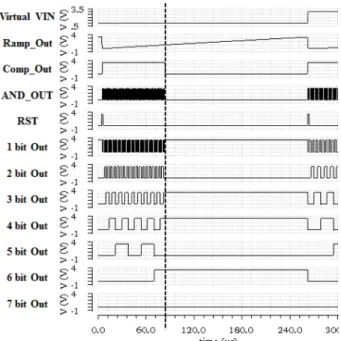
Fig. 10 은 Main_CLK=2[MHz], Virtual UV_VIN=1[V], VIS_IN
=3[V], IR_IN=2[V] 를 인가하였을 때의 시뮬레이션 결과이다. 3 개 센서의 신호처리에 의한 디지털 출력 값을 2진수, 10진수 그 리고 아날로그 신호로 변경한 결과 값을 Table 5에 나타내었다.
제안하는 SSADC는 0.35 μm CMOS 2P4M(2-poly 4-metal) 공 정 규칙에 맞추어 Fig. 11과 같이 레이아웃을 하였다. 전체 크
기는 가로 약 400 μm, 세로 약 300 μm이다. DRC와 LVS tool 을 이용하여 설계한 회로와 레이아웃의 결과를 비교 검증하였다.
4. 결 론
본 논문에서는 자외선, 가시광선, 적외선의 다중 신호처리를 위한 8-bit single slope A/D변환기를 제안하였다. 제안한 SSADC 는 8-bit 해상도와 100 MHz의 처리속도를 가지고 있으며, 기울 기 가변형 램프 발생기를 통해 신호처리의 다양성을 확보하였 다. 또한 세 종류의 이미지 센서를 하나의 SSADC로 신호처리 하기 위해 동작 주파수를 변환하는 클락 분주기와 클락을 선택 할 수 있는 CLK_SW, 입력 신호를 선택 할 수 있는 VIN_SW, 외부 커패시터를 선택할 수 있는 CAP_SW를 설계하여 사용자 가 원하는 이미지를 볼 수 있도록 하였다.
향후 화재 감지 시스템 및 광학 수질 모니터링 시스템 등 자 외선, 가시광선, 적외선 센서를 이용한 복합 이미지 센서가 개 발될 경우 다중 센서 신호처리를 위한 ADC에 도입하여 고집적, 고성능, 저전력에 중요한 역할을 할 것으로 예상된다.
ACKNOWLEDGMENT
This research was supported in part by Kyungpook National Fig. 9. Simulation results of the proposed 8-bit Up Counter(b) block
Fig. 10. Simulation results of the proposed single slope ADC
Table 5. Result value of the proposed single slope ADC Selection external signal 8-bit
D
outBinary number
8-bit D
outDecimal
number
V
out[V]
S1 S0
0 0 01001101 77 1
0 1 11101110 238 3
1 0 10011100 156 2
Fig. 11. Layout of the proposed single slope ADC
University Research Fund, 2012 and in the part by the BK21 Plus project funded by the Ministry of Education, Korea (21A20131600011)
REFERENCES