Portable Metamaterial Structure Antenna for Dual-Band and Polarization-Reconfigurability
Changhyeong Lee, Dajung Han, Heejun Park, Sungtek Kahng
ABSTRACT
This paper presents the design of a palm-sized metamaterial antenna system having reconfigurable polarization as well as dual-band characteristics. Basically, three antennas are laid by 45 degrees in order and excited by a compact metamaterial dual-band power-divider of the in-phase outputs, and the radiated fields of the antennas are mixed to turn the vector of the polarization to another. The validity of the proposed method is verified by observing the in-phase outputs from the odd-numbered power-dividing device for both 900 MHz and 2.4 GHz, and checking the changeable polarization with the antenna gain over 2 dBi for all the polarizations.
Key Words : Metamaterial, Dual-band power-divider, Reconfigurable polarization.
※ This work was supported by ICT R&D program of MSIP/IITP. [The Infrastructure Establishment of 3D Beam Measurement Facilities for 5G antenna using the Millimeter Wave Band]
*Dept. of Info. & Telecomm. Eng. Incheon National University. Incheon, Korea ([email protected]) 접수일자 : 2016년 09월 26일, 최종게재확정일자 : 2016년 9월 29일
I. Introduction
Wireless communication systems have RF power dividers, couplers, filters and relevant parts [1-5]. Fast growing telecommunication industry has pushed microwave technologies to meet the users’ demands, and the power dividers have been developed to cope with the multiple bands for functionality integration, broadband services, so on and so forth [1,2]. Responding to these, a great amount of research has been carried out to produce size-reduced advanced power dividers, and it may be represented by bending and folding, cascaded multi-stages, grid array, slot coupling between layers, discrete loads, etc.
The conventional techniques above expose several shortcomings : additional loss from the elongated geometry, size-limit, and increasing cost due to stack-up fabrication. Alternatively, the dispersion engineering in metamaterial was introduced [3-6]. Caloz brought the CRLH transmission line into the light. They demonstrated the phenomena of the LH, ZOR, and RH with periodic geometry comprising 24 cells of distributed elements [3].
Lumped elements are cascaded in series to generate +90°
or -90° and put in couplers and power dividers. Similarly, F. Martin inserted a pair of slot rings under each of the arms of the Wilkinson power divider for the purpose of reducing the overall size[4].
To overcome the drawbacks of the previously mentioned metamaterial and ordinary techniques, an improved method is provided for a smaller and advanced component. A novel 3-way dual-band CRLH power divider is designed to have a very small area and the equal power division and in-phase outputs. First, CRLH 2:1-unequal and 1:1-equal dual-band power dividers are separately designed. Second, the inputs of the equal block are connected to an output of the unequal block to be an initial 1:1:1 power divider. At this point, this initial configuration has phase errors between the output ports.
Hence, third, a dual-band phase compensation line is designed, consisting of a transmission line as the RH part and lumped elements as the LH part (named hybrid CRLH line), and is added to eliminate the output-port phase error. The design is performed with the circuit analysis and full-wave simulation. And it is fabricated 1:1:1 power divider. The polarization changeable antenna system is set up on the basis of the power divider. A set of different linear polarizations can be created by the combination of more than two polarizations from the adjacent radiating elements. So, the three antennas are fed by the power divider, and switching the three ways gives the combination of the E-field vectors. The polarization reconfigurability is observed, while the radiation performance should be acceptable.
Ⅱ. The elemental and complete dual-band equi-phase 3-way power-dividers
As is clearly stated, a novel three-way power divider to be made compact as the CRLH characteristics is schematized in the following figure.
Fig. 1. The schematic of the proposed power divider
Fig. 1 shows that the unequal power divider block is connected to the equal block, and both the blocks will be realized as printed CRLH devices of small footprints. The small CRLH dual-band structure is based on CRLH phase-shift line. The equivalent circuit of the aforementioned phase-shift lines for the dual-band unequal and equal power-divider blocks in Fig.1 is illustrated as follows.
(a)
(b)
Fig. 2. The equivalent circuits of the CRLH phase-shift line and the unequal power divider (a) phase- shift line (b) unequal power divider.
Fig. 2(a) is used to create phase Φ1 for a lower frequency f1 and phase for a higher frequency f2 for an arbitrary ratio f2 to f1.These phases and frequencies make the simultaneous equations containing the circuit elements, and mathematical manipulation renders L’s and C’s as given in the equations[5] where ω1=2πf1 andω2=2πf2, and Zc
becomes Zk1 for one path and Zk2 for another path in an unequal power divider. In the present case, applying Φ
1=+90° at f1=960MHz and Φ2 = -90° at f2=2.4GHz to equation1 for Fig.2(a) results in the CRLH phase-shift line of the following data.
(a)
(b)
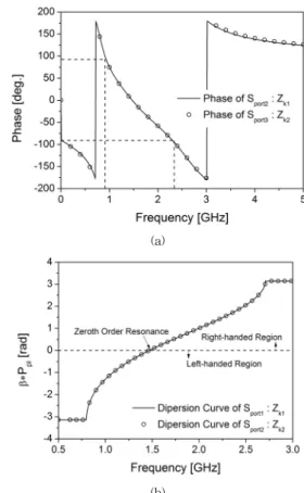
Fig. 3. The characteristics of the CRLH phase-shift line (a) phase (b) dispersion diagram
Fig. 3(a) shows the phase as wanted as applying Φ
1=+90° at f1=960MHz and Φ2=-90° at f2=2.4GHz. This implies that this CRLH phase-shift line can be substituted for the quarter-wave long arms for the dual-band performance. Fig.3(b) of the dispersion diagram presents the LH region including f1, the ZOR, and the RH region including f2 as a metamaterial property. This phase-shift line is input to the upper and lower paths of the dual-band unequal power divider as Fig.2(b). The characteristic impedance for each path is obtained with the following formulae, once we decide the power division ratio.
(1)
Keeping in mind the connection to the equal block afterwards to make the 3-way power divider, the present unequal block should have the power division ratio of 2:1 with Zk1=51.5Ω and Zk2=103Ω. These impedance values are put into eqn.(1) with the previously mentioned phases, and the circuit elements of the phase-shift lines for both the paths are found : CR ,CL, LR, and LL are 4.7pF, 2.0pF, 5.9nH, 2.5nH in the 51.5-Ω path, and CR, CL, LR, and LL
are 2.4pF, 1.0pF, 11.8nH, 5.0nH in the 103-Ω path. These lead to Fig.3, actually. To observe the frequency response of the overall unequal block in Fig.2(b) taking into account the CRLH phase-shift lines of Fig.3, the upcoming even-and odd-mode analysis techniques are adopted.
(a)
(b)
Fig. 4. The circuit models on the even- and odd-modes (a) Even-mode (b) Odd-mode
Fig. 4(a) comes from Fig. 2, as ports 2 and 3 are excited with the in-phase signals and the bi-section line is treated as an open-circuited state. Fig. 2 becomes Fig. 4(b) in the assumption that the out-of-phase signals are fed into ports 2 and 3, and the axis of anti-symmetry is considered short-circuited. This applies to both the impedance lines.
The frequency response of Fig. 2(b) will be given in the form of s-parameters following the formulation in reference 5. Therefore, the s-parameters are plotted as the frequency responses of the unequal and equal dual-band power dividers.
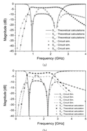
The predicted performance of the 2:1 unequal power divider is shown in Fig. 5(a) where |S21|is -4.7dB and -1.7dB at 960MHz and 2.4GHz as wanted. |S21| is equal to |S31|, and the result of our code for the derived equations overlaps that of the commercial circuit analysis tool. Likewise, Fig. 5(b) unveils the perfect agreement between the coding and the commercial program, and
|S21|=-3dB and |S31|=-3dB as the 1:1 power division at the two target frequencies. The mathematical derivation has been validated and the se elementary blocks will be incorporated for the 1:1:1 power division.
In this section, the unequal and equal blocks are inter- connected to form the three equal outputs, and realized and tested in the full-wave simulation. Let alone, since one output is different from the remaining outputs in
terms of phase for each of the two frequencies, the phase correction will be attained by using an efficient way.
(a)
(b)
Fig. 5. The circuit simulated frequency responses of the unequal and equal power dividers for the dual- band application (a) s-parameters of the unequal block (b) s-parameters of the equal block
The unequal and equal power-dividing circuits of Fig.
4 and Fig. 5 are physically implemented by taking the steps to consider full-printing, and the input of the equal block is fed by the output of the 103-Ω path of the unequal dual-band power divider.
Fig. 6. The initial form of the 3-way CRLH dual-band power divider
Fig. 6 presents the physical shape of the initial 1:1:1 power divider. The geometrical parameters are W, L1_L, W_F, L_F, L2_L2, G_F2, L1_L3, W_F3, L_F3, L, L2_L, G_F, L1_L2, W_F2, L_F2, L2_L3, and G_F3 as 30.6 mm, 3.5 mm, 0.4 mm, 5 mm, 5.3 mm, 0.1 mm, 3.1 mm, 0.4 mm, 5 mm,
43.7 mm, 7.5 mm, 0.2 mm, 3.5 mm, 0.6 mm, 5.6 mm, 4.1 mm, and 0.3 mm, respectively, with FR4 of εr=4.4 as the substrate. The performance is given as.
(a)
(b)
(c)
(d)
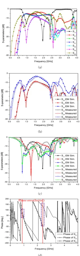
Fig. 7. The full-wave simulated and measured results of the proposed dual-band compact 3-way power divider (a) power-division performances (b) inter-port isolation performances (c) reflection coefficients (d) phases at the outputs
In Fig. 7(a), equal power division to the 3 output ports is achieved with nearly -6dB of |S21|, |S31|, and |S41| at 960MHz and 2.4GHz simultaneously in the EM simulation and measurement. Fig. 7(b) and (c) have |S23|, |S23| and |S34|, and |Sii| below -12dB at f1 and f2 more or less. But, while the phases of S31 and S41 are the same, they differ from the phase of S21 as marked in Fig. 7(e). This error should be removed. And the location of port 2 in Fig. 6 should be corrected for better RF cabling. So, the phase errors at f1
and f2 should be mended with considering the new position of port 2. Since port 2 is located on the opposite side from ports 3 and 4, and off the extension line from port 1 in Fig.
6, port 2 can be moved to the same side of port 4.
(a)
(b)
Fig. 8. The 3-way dual-band power divider with a new location of port 2 and the insertion of the phase compensating hybrid CRLH line for the in-phase outputs (a) phase correcting line added to the layout as the finalized 3-way dual-band power divider (b) In-phase outputs obtained.
Fig. 8(a) shows a CRLH line is inserted into the output of the 103 Ω path of the unequal block to the new port 2, and the phase errors (∆Φ1 and ∆Φ2) between S21 and S31
at f1 and f2 are found 14.5° and 168° as observed in Fig. 8(b).
To make a compact dual-band phase-shift line for ∆Φ1
and ∆Φ2, a hybrid CRLH structure is designed with L_R, W_L, L and C as 15 mm, 1.2 mm, 11 nH, and 1 pF, respectively. Hence, the in-phase outputs are accomplished as Fig. 8(b)
Ⅲ. Change in polarization of the antenna system
The reconfigurability in polarization is schematized by the combinations of the E-field polarizations from the antennas placed in Fig. 9.
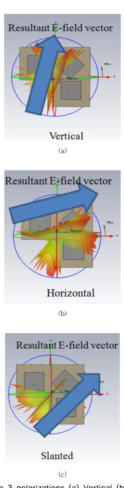
Fig. 9. The 3-way dual-band power divider feeds three patch antennas for combining polarization vectors.
The patches are placed with a 45-degree inclination from the patch of port 2 to the one of port 4 so that the polarizations from neighboring radiators can be summed.
It is planned that the vertical polarization becomes the strongest, when ports 2 and 3 are excited. On the contrary, the horizontal polarization becomes dominant with ports 3 and 4 excited. Besides, when ports 2, 3 and 4 are excited, a slanted polarization is expected. For this multiple purpose, these odd-number of the patches should be linked to the equi-phase and equi-magnitude outputs of the three-way power divider, which should not be larger than the footprint of the all the patches. Here are the design results.
For the sake of convenience, 2.4 GHz patches(area of 28 mm-by-28 mm) are selected not as a dual-band structure.
In this verification, a polarization-agile 2.4-GHz WiFi access point indoor equipment is targeted. Because the power-divider can handle the 900 MHz in the same way for 2.4 GHz, if the UHF-band antenna is chosen, almost the same properties will be obtained. Fig. 10(a) shows the vertical polarization with ports 2 and 3 turned on, where the vertical component of the diagonally directed surface-current of port 3 antenna is additive. The horizontal polarization is seen in Fig. 10(b) where the horizontal components of the E-field s from port 3 and 4-antennas constructively interfere. Fig. 3(c) presents the 45-deg. slanted polarization contributed by the one directly from port 3-patch and the other from the perpendicular vectors from port 2 and port 4 patches.
(a)
(b)
(c)
Fig. 10. The 3 polarizations (a) Vertical (b) Horizontal (c) Slanted.
Ⅳ. conclusion
A compact dual-band three-way power-divider was designed. This excites the patches to have a reconfigurable-polarization property. From the test, the function to change the polarization was checked. It is applicable to agile indoor access point antenna systems.
Acknowledgment
This work was supported by ICT R&D program of MSIP/IITP. [The Infrastructure Establishment of 3D Beam Measurement Facilities for 5G antenna using the Millimeter Wave Band]
References
[1] Z. Sun, L. Zhang, Y. Yan, and H. Yang, "Design of unequal dual band Gysel power divider with arbitrary termination resistance," IEEE Trans. on MTT, vol. 59, no. 8, pp.
1955-1962, Aug. 2011.
[2] H. Oraizi, A. -R. Sharifi "Optimum design of asymmetrical multi section two-way power dividers with arbitrary power division and impedance matching," IEEE Tran. on MTT, pp.
1478-1490, Jun. 2011.
[3] C. Caloz, T. Itoh, Electromagnetic Metamaterials: Transmission Line Theory and Microwave Application, New Jersey : John Wiley & Sons, 2006.
[4] R. Marques, F. Martin and M. Sorolla, Metamaterials with Negative Parameters : Theory, Design, and Microwave Application, New Jersey : John Wiley and Sons, 2008.
[5] D.-J. Eom and S. Kahng, "Fully Printed Dual-Band Power Divider Miniaturized by CRLH Phase-Shift Lines," ETRI Journal, vol.35, no.1, pp.150-153, February 2013.
[6] K. Jang, S. Kahng, J. Jeon, and Q. wu "Compact Dual-Band Three-Way Metamaterial Power-Divider with a Hybrid CRLH Phase-Shift Line", JEES, Vol.14, NO.1, pp.15-24, March 2014.
저자
이 창 형(Changhyeong Lee) 비회원
․2016년 2월 : 인천대학교 전자공학과 (공학사)
․2016년 3월 ∼ 현재 : 인천대학교 정보 통신공학과 석사과정
<관심분야> : 초고주파부품 및 안테나, 메타재질구조이론 및 응용
한 다 정(Dajung Han) 비회원
․2016년 2월 : 인천대학교 전자공학과 (공학사)
․2016년 3월 ∼ 현재 : 인천대학교 정보 통신공학과 석사과정
<관심분야> : 초고주파부품 및 안테나, 메타재질구조이론 및 응용
박 희 준(Heejun Park) 비회원
․2010년 3월 ∼ 현재 : 인천대학교 정 보통신공학과 학사과정
<관심분야> : 초고주파부품 및 안테나, 메타재질구조이론 및 응용
강 승 택(Sungtek kahng) 정회원
․2000년 2월:한양대학교 전자통신 공 학박사
․2000년 4월:한양대학교 산업과학연 구소 연구원
․2004년 2월:한국전자통신연구원통신 위성개발센터선임연구원
․2004년 ∼ 현재:인천대학교 정보통신공학과 교수
․2007년 ∼ 현재:송도국방벤처 자문교수
․2007년 ∼ 현재:한국통신학회 마이크로파 및 전파연구회 간사∼위원장, 한국전자파학회 편집위원, 국제이사
․2014년 12월 대한전기학회 학술상 수상 광파 및 전자파분야 <관심분야> : 전자파 수치해석 및 응용, EMI/EMC 대책, 초
고주파 부품 및 안테나설계, 메타재질구조이론 및 응용