A CMOS Impulse Radio Ultra-Wideband Receiver for Inner/Inter-chip Wireless Interconnection
Nguyen Chi Nhan
★,Duong Hoai Nghia
*and Dinh Van Anh
**Abstract
This paper presents a CMOS impulse radio ultra-wideband (IR-UWB) receiver implemented using IBM 0.13um CMOS technology for inner/inter-chip wireless interconnection. The IR-UWB receiver is based on the non-coherent architecture which removes the complexity of RF architecture (such as DLL or PLL)and reduces power consumption. The receiver consists of three blocks: a low noise amplifier (LNA) with active balun, a correlator, and a comparator. Simulation results show the die area of the IR-UWB receiver of 0.2mm2, a power gain (S21) of 12.5dB, a noise figure (NF) of 3.05dB, an input return loss (S11) of less than -16.5dB, a conversion gain of 18dB, a NFDSB of 22. The receiver exhibits a third order intercept point (IIP3) of -1.3dBm and consumes 22.9mW of power on the 1.4V power supply.
Keywords: UWB receiver, non-coherent receiver, inner/inter-chip communications.
★Corresponding author: Department of Physics and Electronics, University of Science, VNU-Hochiminh City, Vietnam ([email protected])
* Faculty of Electrical and Electronics Engineering, University of Technology, VNU Hochiminh City, Vietnam ([email protected])
** Department of Electrical and Computer Engineering, University of Saskatchewan, Saskatoon, Canada ([email protected])
Manuscript received May. 13, 2013; revised Jun. 13, 2013 ; accepted Jun 17. 2013
Ⅰ. Introduction
Impulse radio ultra-wideband (IR-UWB) is an attractive wireless transmission technology which enables high band-width short distance communications. The UWB communications does not require expensive and complex components for modulation and demodulation and IF stages, and thus reducing cost, size, weight, and power consumption of the system [1-3]. In 2002, the Federal Communications Commission (FCC) released an unlicensed frequency range of 7.5GHz, from 3.1GHz to 10.6GHz, for the commercial short-range wireless communication applications [4]. In recent years, a
number of research works focused on inner/inter-chip wireless interconnections by using IR-UWB communicationsdue to its low complexity and low power [5-17]. In IR-UWB systems, the receiver is an important component and is more complex than the transmitter. There are basically two different types of receivers employed in IR-UWB systems namely coherent receiver and non-coherent receiver. The coherent and non-coherent architectures have been reported in the literature [5-7]. Both coherent and non-coherent receivers correlate the received pulse first, such that the center frequency is down-converted to baseband. The difference is that in a coherent receiver, the received pulse correlates with a local template pulse and needs many timing synchronization circuit blocks which increases system complexity. In a noncoherent receiver, the received pulse correlates with itself andremoves the complexity of RF architecture (DLL or PLL)and reduces power consumption.
In this paper, an IR-UWB based non-coherent single chip CMOS receiver is presented. The on chip receiver is implemented using 0.13um CMOS technology. The receiver covers 6.0~10.6 GHz that is the high frequency band of the UWB system.
Ⅱ. IR-UWB Receiver Circuit Design
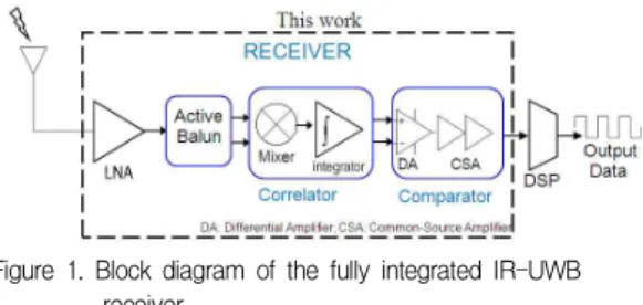
The proposed IR-UWB receiver employs the non-coherent receiver architecture. Figure 1 shows the block diagram of the fully integrated IR-UWB receiver.
Figure 1. Block diagram of the fully integrated IR-UWB receiver
The received UWB signal is amplified through a low-noise amplifier (LNA) with an active balun. This amplifier provides a constant gain optimized around the operation frequency of 8.0 GHz. After first being amplified by the LNA, the received pulse is then self-correlated by a correlator, and then sent to a comparator for digital quantization.
A. LNA and Active Balun: The UWB LNA design uses resistive feedback current reuse technique. The design was implemented in the IBM 0.13um CMOS technology with appropriate impedance matching and noise/power optimizations. The LNA achieves up to 12.5dB power gain with a noise figure (NF) of 3.05dB over the UWB 3.1-10.6GHz frequency range.
Figure 2 shows the schematic of LNA.
RF
In
M1
M2
Out
M3
R1
R2
L2
L1
C1
C2
C3
Figure 2. Schematic diagram of the LNA
The input inductor L1 is added to compensate for the parasitic capacitors of M1 and M2 transistors at
high frequencies. A resistive feedback buffer with peaking inductor load is coupled with the reuse UWB stage through capacitor C3 to drive the 50Ohm output load. Besides, in the resistive feedback current reuse configuration (the first stage), loading the NMOS transistor M1 with the PMOS transistor M2 allows the circuit to operate under lower supply voltage than resistive load configuration.
A two-cascode stage active balun (Figure 3)is used to convert the single-ended output of the LNA to differential signals. The output of M4 connects to M6 and the input of the second cascode. Since vgs5=-vgs6, two balanced differential outputs can be achieved if gm5=gm6
Figure 3. Schematic diagram of the active balun
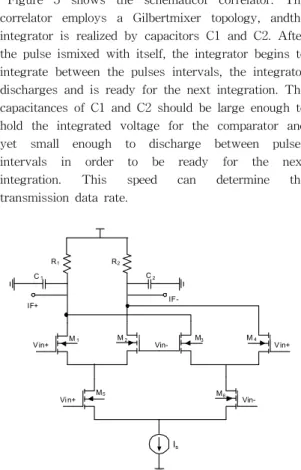
B. Correlator: The output of the LNA must be correlated - multiplied and then integrated in order to detect the energy of the received signal. Figure 4 shows the block diagram of correlator. Equation (1) shows the output signal of correlator.
Figure 4. Block diagram of the correlator
(1)
where r0(t) is the output signal of the correlator,
( )
00
0 t ( ). template( )
t T
r t r t S t dt
=
ò
-r(t) is the input signal of the correlator and Stemplate(t) is the template signal.
Figure 5 shows the schematicof correlator. The correlator employs a Gilbertmixer topology, andthe integrator is realized by capacitors C1 and C2. After the pulse ismixed with itself, the integrator begins to integrate between the pulses intervals, the integrator discharges and is ready for the next integration. The capacitances of C1 and C2 should be large enough to hold the integrated voltage for the comparator and yet small enough to discharge between pulses intervals in order to be ready for the next integration. This speed can determine the transmission data rate.
R1
M1
Vin- R2
V in+
M5
M3
M2
C1
M6
C2
M4
Is Vi n+
V in+
Vin-
IF+ IF-
Figure 5. Schematic diagram of the correlator
C. Comparator: After the received signal is squared and integrated by the correlator, a comparator compares it with a reference voltage and performs digital quantization. However the comparator output is a return-to-zero (RZ) signal which needs to be converted to a non-return-to-zero (NRZ) signal that can synchronize with the baseband clock. In a coherent receiver, a DLL/PLL is usually introduced to perform synchronization between the received pulse and the local pulse, needing precision on the order of several tens of picoseconds. However, in a noncoherent receiver, the RZ signal quantized by the comparator exhibits a duty cycle on the order of nanoseconds. Therefore, a low jitter DLL/PLL is no longer necessary and a sliding correlator is employed.
The technique reduces complexity of the receiver.
The topology of the comparator consists of differential amplifier with buffering inverter and common-source amplifier. The block diagram and the schematic diagram of the comparator are shown in Figure 6 and Figure 7, respectively.
Figure 6. Block diagram of the comparator
M3
M1
M4
Idc 1 M5
M2 M6
M7 M8
M9 M10
Idc2 M11
M1 2 M1 3
Idc3 M14 V+
V -
O u tpu t
C1
Figure 7. Schematic diagram of the comparator
The comparator is based on a differential amplifier with two differential inputs (va and vb ).
-The input voltage is in the differential-mode:
(2)
-The input voltage is in the common-mode:
(3)
From (2) and (3),
ID a b
V = v - v
2
a b
IC
v v
V +
=
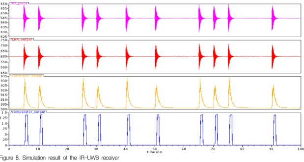
Figure 8. Simulation result of the IR-UWB receiver
(4)
-The output voltage:
(5)
where
AVD is amplification factor in the differential-mode.
AVC is amplification factor in the common-mode
Ⅲ. Simulation Results
The IR-UWB receiver was designed and simulated using Cadence tools applicable in IBM 0.13um CMOS technology. The simulation result of the IR-UWB waveforms is shown in Figure 8. The waveforms are listed as: A is the received signal from the antenna,
B is the output of the LNA, C is the output of the correlator, and D is the output of the comparator.
The amplitude of output voltage of the correlator is different (e.g. at 6ns and 11ns or 26ns and 31ns) because they were affected by the amplitude of impulse radio UWB receiver. In the comparator we used the op-amps and a vdc (vpulse) with amplitude of 1.4V for UWB receiver. The op-amps
Figure 9. Layout of the IR-UWB receiver
can amplify almost all signals that the amplitude of output voltage of equal mico volt. The output signal of the comparator is the bit stream.
Figure 9 shows the layout view of the IR-UWB receiver. The area of the receiver is about 0.2mm2. The power consumption of the receiver is 22.9mW for the 1.4V supply voltage. Table 1 shows the parameters of the IR-UWB receiver.
2
ID
b IC
v =V -V 2
ID
a IC
v =V +V and
( )
2
a b
out VD ID VC IC VD a b VC
v v
V A V A V A v v A æ + ö
= ± = - ± ç ÷
è ø
Table 1: COMPARISON WITH PREVIOUSLY REPORTED IR-UWB RECEIVERS
Parameters This
work [16] [17]
Technology 0.13um CMOS
0.13um CMOS
0.18um CMOS B a n d w i d t h
(GHz) 6.0-10.6 3.1-10.6 3.1-5.0
S11 (dB) < -16.5 < -10 < -9.1 Gain Max(dB)
(S21) 12.5 17 < 30
NF (dB) 3.05 4 to 5.1 4.3
C o n v e r s i o n
Gain(dB) 18 29 -
IIP3 (dBm) -1.3 -14 -
Power (mW) 22.9 31.5 21.9
Chip Area
(mm2) 0.2 - 1.8
Ⅴ. Conclusion
In this work, a CMOS non-coherent IR-UWB receiver was designed and simulated using Cadence tool with IBM 0.13um CMOS technology for inner/inter-chip wireless interconnection. The results show a promising design for 3-D chip wireless communications due to its low complexity and small chip area. Appropriate choices of the charge and discharge capacitance in the correlator will further more increase the system data rate.
References
[1] M. Ghavami, L. B. Michael, R. Kohno,
"Ultra Wideband Signals and Systems in Communication Engineering," John Wiley & Sons, 2004.
[2] Faranak Nekoogar, "Ultra-Wideband Communications: Fundamentals and Applications,"
Prentice Hall Pearson Education, 2005.
[3] Immoreev I. Y, "Practical application of Ultra-Wideband radars," IEEE UltraWideband and Ultrashort Impulse Signals, pp. 44-49, Sept. 2006.
[4] Federal Communications Commission,"First report and order, revision of part 15 of the
commission’s rules regarding ultra wideband transmission system," Washington, DC,ET Docket 98-153, 2002.
[5] Tiuraniemi, S., Stoica, L.; Rabbachin, A., and Oppermann, I., "Front-end receiver for low power, low complexity non-coherent UWB communication system," IEEE International Conference on Ultra-Wideband, pp. 339-343, Sept. 2005.
[6] Yuanjin Zheng, Yan Tong, Jiangnan Yan;
Yong-Ping Xu, Wooi Gan Yeoh, and Fujiang Lin, "A low power non-coherent CMOS UWB transceiver ICs," IEEE Radio Frequency Integrated Circuits (RFIC) Symposium, Digest of Papers, pp. 347-350, June 2005.
[7] Yang Tong, Yuanjin Zheng, and Yong-Ping Xu,
"A Coherent Ultra-Wideband Receiver IC System for WPAN Application," IEEE International Conference on Ultra-Wideband, pp. 60-64, Sep. 2005.
[8] Vitaliy Zhurbenko,"Advanced Microwave Circuits and Systems, Chapter 3: Current reuse topology in UWB CMOS LNA,"In-Teh Open Access Publisher, ISBN 978-953-307-087-2, 2010.
[9] Yi-Jing Lin, Shawn S. H. Hsu, Jun-De Jin, and C. Y. Chan, "A 3.1–10.6 GHz Ultra-Wideband CMOS Low Noise Amplifier With Current-Reused Technique," IEEE Microwave And Wireless Components Letters, Vol. 17, No. 3, 2007.
[10] Chunjiang Tu, Boan Liu, Hongyi Chen,"An Analog Correlator for Ultra-Wideband Receivers,"
EURASIP Journal on Applied Signal Processing, pp. 455-461, 2005.
[11] Shen, D.; Fujiang Lin; Wooi Gan Yeoh, "An analog correlator with dynamic bias control for pulse based UWB receiver in 0.18/spl mu/m CMOS technology," Radio Frequency Integrated Circuits (RFIC) Symposium, IEEE , pp 11-13,June 2006.
[12] Hsien-Yuan Liao, Ching-Ming Tseng, and Hwann-Kaeo Chiou, "Lossy LC Ladder Matching Network For Ultra-Wideband CMOS Gilbert Cell Mixer Design," IEEE Microwave And Optical Technology Letters, Vol. 50, No. 1, January 2008.
[13] Goo-Young Jung, Jae-Hoon Shin, and Tae-Yeoul Yun, "A Low-Noise UWB CMOS Mixer Using Current Bleeding And Resonant Inductor Techniques," Microwave And Optical Technology Letters, Vol. 49, No. 7, July 2007.
[14] Chung-Ru Wu, Hsieh-Hung Hsieh, and
Liang-Hung Lu, "An Ultra-Wideband Distributed Active Mixer MMIC in 180nm CMOS Technology,"
IEEE Transactions On Microwave Theory And Techniques, Vol. 55, No. 4, April 2007.
[15] S. Jeong-Bae, K. Jong-Ha, S. Hyuk, and Y.
Tae-Yeoul, "A Low-Power and High-Gain Mixer for UWB Systems," Microwave and Wireless Components Letters, IEEE, Vol. 18, pp. 803-805, 2008.
[16] Bo Shi, Michael Yan Wah Chia, "Design of a CMOS UWB Receiver Front-End With Noise- Cancellation and Current-Reuse," Proceedings of 2010 IEEE International Conference on Ultra-Wideband (ICUWB2010), Vol.1, pp. 1 – 4, 2010.
[17] Caixia Chen, Manh Anh Do, Kiat Seng Yeo and Chirn Chye Boon, "A Low Power UWB Direct Conversion Receiver with Pulse Detectors,"
Proceedings of 2009 International on SoC Design Conference (ISOCC), pp. 17 – 20, 2009.
BIOGRAPHY
NguyenChiNhan
was born in Vietnam on April 11, 1977. He received his B.S. and M.Sc. degrees in Physical Electronics from University of Science, Vietnam National University - Ho Ch Minh City (VNU-HCMC), in 1999 and 2003, respectively. He is currently working on his Ph.D.
course in the Department of Physics and
Electronics at University of Science, VNU-HCMC.
His research field of interest includes wireless communications (RF, UWB), VLSI Design, Integrated Circuit Design and Embedded System.
DuongHoaiNghia
was born in Ben Tre, Vietnam, on May 31st1957. He received the B.E. degree in Electrical and Electronics Engineering from the Ho Chi Minh city University of Technology, Vietnam, in 1981, and the M.S. and Ph.D. degrees in Automatic Control from the Institut National Polytechnique de Grenoble, France in 1989 and 1993, respectively. He was a postdoctoral researcher at the Laboratoire d’Automatique de Grenoble (CNRS/INPG), France, from 1993 to 1995.
Since 1981 he serves as an Instructor in the Department of Electrical and Electronics Engineering at the University of Technology, Vietnam National University, Ho Chi Minh city.
From 1997 to 2002 he was head of the Division of General Electrical-Electronics Engineering. Since 2002 he is a Vice Dean of the Department. Since 2007 he is an Associate Professor. He is a member of the IEEE. His research interests are in the area of system identification, multivariable control, nonlinear control, and soft computing.
AnhDinh
received his M.Sc. and Ph.D. in electrical engineering at the University of Regina, Canada, in 1997 and 2000, respectively. Dr.
Dinh is currently at the Department of Electrical and Computer Engineering, University of Saskatchewan, Canada as an AssociateProfessor.
His research interests are in RF circuits applicable to wireless communications and biosensors. He also designs equipment for health research.
![Table 1: COMPARISON WITH PREVIOUSLY REPORTED IR-UWB RECEIVERS Parameters This work [16] [17] Technology 0.13um CMOS 0.13umCMOS 0.18umCMOS B a n d w i d t h (GHz) 6.0-10.6 3.1-10.6 3.1-5.0 S11 (dB) < -16.5 < -10 < -9.1 Gain Max(dB) (S21) 12.5 17 &l](https://thumb-ap.123doks.com/thumbv2/123dokinfo/4676718.501295/5.772.67.374.194.459/table-comparison-previously-reported-receivers-parameters-technology-umcmos.webp)
