• 검색 결과가 없습니다.

Growth of ZnSnO<sub>3</sub> Thin Films on c-Al<sub>2</sub>O<sub>3</sub> (0001) Substrate by Pulsed Laser Deposition

N/A
N/A
Protected

Academic year: 2021

Share "Growth of ZnSnO<sub>3</sub> Thin Films on c-Al<sub>2</sub>O<sub>3</sub> (0001) Substrate by Pulsed Laser Deposition"

Copied!
6
0
0

로드 중.... (전체 텍스트 보기)

전체 글

(1)

DOI: http://dx.doi.org/10.4313/JKEM.2014.27.5.297 ISSN 1226-7945 (Print), 2288-3258 (Online)

Growth of ZnSnO 3 Thin Films on c-Al 2 O 3 (0001) Substrate by Pulsed Laser Deposition

Trung Tran Manh

1

, Jae-Ryong Lim

1

, and Soon-Gil Yoon

1,a

1

Department of Materials Science and Engineering, Chungnam National University, Daejeon 305-764, Korea

(Received April 10, 2014; Revised April 21, 2014; Accepted April 23, 2014)

Abstract: La

0.5

Sr

0.5

CoO

3

(LSCO) electrode thin films with a resistivity of ∼ 1,600 µΩcm were grown on c-Al

2

O

3

(0001) substrate. ZnSnO

3

(ZTO) thin films with different thicknesses were directly grown on LSCO/c-Al

2

O

3

(0001) substrates at a substrate temperature that ranged from 550 to 750℃ using Pulsed Laser Deposition (PLD). The secondary phase Zn

2

SnO

4

occurred during the growth of ZTO films and it became more significant with further increasing substrate temperature. Polarization-electric-field (P-E) hysteresis characteristics, with a remnant polarization and coercive field of 0.05 µC/cm
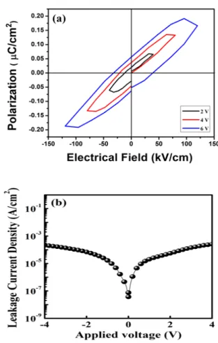
2

and 48 kV/cm, respectively, were obtained in the ZTO film grown at 700℃ in 200 mTorr.

Keywords: Piezoelectric, ZnSnO

3

thin film, Ferroelectric thin films

1. INTRODUCTION


NCS (non-centrosymmetric) oxides [1] have attracted considerable attention due to their unique symmetry-dependent and spontaneous polarization properties, which are technologically significant and are the basis of numerous applications in ferroelectricity, piezo-electricity, and nonlinear optics [2]. ZnO is well known as environmentally friendly and piezoelectric material [3]. Besides ZnO, there are still many lead-free piezoelectric materials in the NCS group that have been discovered recently, especially in terms of perovskite structure

such as: BaTiO

3

[4], (K,Na)NbO

3

[5-7], (1−x)Ba(Zr

0.2

Ti

0.8

)O

3

-x(Ba

0.7

Ca

0.3

)TiO

3

[8], and etc.

In spite of the success in lead-based piezoelectric

a. Corresponding author; [email protected]

Copyright ©2014 KIEEME. All rights reserved.

This is an Open-Access article distributed under the terms of the Creative Commons Attribution Non-Commercial License (http://creativecommons.org/licenses/by-nc/3.0) which permits unrestricted non-commercial use, distribution, and reproduction in any medium, provided the original work is properly cited.

materials (i.e. lead zirconate titanate, 0.65PbMg

1/3

Nb

2/3

O

3

-0.35PbTiO

3

[9,10]) due to their high polarization and piezoelectric performance as transducers [11], a consistent effort has been taken to replace Pb-based materials with some as yet undiscovered lead-free materials [12] that would be more environmentally friendly and enable new piezoelectric applications for mechanical energy harvesting. Recently, Inaguma reported a lead-free LiNbO

3

- type ZnSnO

3

using a high-pressure (∼7 GPa) synthesized environment [2] and Jyh Ming Wu successfully fabricated ZnSnO

3

microbelts given an output voltage and current of 100 mV and 30 nA, respectively [13].

Until now, there are only few reports on the

preparation and electrical properties of ZnSnO

3

thin

films [14-16]. To the best of our knowledge, this

is the first report on the growth of ZTO thin films

on c-Al

2

O

3

(0001) substrates using the PLD

method. In the present study, 500-nm thick ZTO

films were deposited on c-Al

2

O

3

(0001) substrates

(2)

deposition, and the electrical properties of the heterostructure ZTO/LSCO/c-Al

2

O

3

(0001) films grown at various temperatures are discussed.

2. EXPERIMENTS

The ZnSnO

3

/LSCO/c-Al

2

O

3

thin films were grown at a substrate temperature within the range of 550 to 750℃ on c-Al

2

O

3

(0001) substrates by pulsed laser deposition using a pulsed KrF excimer laser (248nm, Lamda Physik COMPex-Pro 201). A ZnSnO

3

ceramic target with a diameter of 2.54 cm was used for deposition of the ZTO thin films. The ZnSnO

3

target was fabricated by processing stoichiometric mixture of ZnO (Aldrich 99.999%) and SnO

2

(Aldrich 99.995%) powder at the desired 1/1 ratio. Powder was ball-milled in ethanol for 4 h to insure homogeneous distribution. Pellets with a diameter of 1 inch were unaxially pressed without binder. The samples were calcined at 850℃

and sintered at 1,300℃ in ambient air for 12 h.

After the base pressure reached 5×10

-6

Torr, the substrate temperature was set to various temperatures with an oxygen partial pressure of 200 mTorr during the deposition of a ZnSnO

3

thin film. The c-Al

2

O

3

(0001) substrates were attached to a heated plate with silver paste in order to maintain a uniform temperature. The details of the conditions for the deposition of the ZTO/LSCO/

c-Al

2

O

3

substrates are summarized in Table 1.

After deposition, high-purity oxygen was introduced into the growth chamber up to 5 Torr and then the films were cooled naturally to room temperature.

Film thicknesses were measured using cross-sectional scanning electron microscopy (SEM) images. The phase of the heterostructure was investigated by θ ∼2 θ , using a high-resolution X-ray diffraction (HRXRD, Rigaku RINT2000).

The resistivity of the LSCO thin films was measured by an electrometer (CMT-SR 1000) using a four-point probe.

grown on c-Al

2

O

3

(0001) substrates.

Deposition parameters LSCO ZTO Target La

0.5

Sr

0.5

CoO

3

ZnSnO

3

Deposition temperature (℃) 450∼650 550∼750

Film thickness (nm) 100, 200 500

Deposition pressure (Torr) 0.3 0.2

Energy density (J/cm

2

) 1.5 1.5

Conventional photolithography was used to pattern the Pt –squares top electrodes of 100 µm in length and sputter-deposition implemented in a commercial dc magnetron sputtering system. The polarization vs.

electric field (P-E) curve of the films was measured using an RT66A ferroelectric tester (Radiant Technology) operated in the virtual ground mode.

3. RESULTS AND DISCUSSION

The LSCO films were prepared on c-Al

2

O

3

(0001) substrates to determine the influences of substrate temperature. The studied ranges were 450

∼650℃ under 300 mTorr oxygen pressure.

Fig. 1. X-ray diffraction patterns of LSCO/c-Al

2

O

3

.

(3)

Fig. 2. (a) Surface resistivity of the LSCO thin films deposited in 300 mTorr oxygen at different substrate temperatures with various thicknesses and (b) grain size and surface resistivities of the LSCO thin films deposited in 300 mTorr oxygen at different substrate temperatures, measured at room temperature.

(0001) deposited at oxygen pressures of 300 mTorr and different temperatures (a) 450℃, (b) 500℃, (c) 550℃, (d) 600℃, and (e) 650℃, the inset shows the morphology of LSCO film grown at 550℃.

Fig. 1 shows θ ∼2 θ XRD patterns for a series of LSCO thin films deposited on c-Al

2

O

3

(0001) substrates at different temperatures. The film grown at 500℃ exhibits a small peak (111) from LSCO, and become higher with further increasing temperatures.

The films present different room temperature electrical resistivity values depending on the processing conditions, and a low resistivity value is important for the use of LSCO as an electrode.

Fig. 3. X-ray diffraction patterns of ZTO/LSCO/c-Al

2

O

3

(0001) heterostructure deposited at oxygen pressures of 200 mTorr and different temperatures (a) 600℃, (b) 700℃, and (c) 750℃.

Fig. 2(a) shows the electrical property corresponding to the series of temperatures and thickness of film measured by the classical four-probe method at room temperature. As can be seen in this figure, the thicker (200 nm) films show lower resistivity than the thinner (100 nm) films with different deposition temperatures. A plot of the resistivity and grain size as a function of growth temperature of LSCO films as shown in Fig. 2(b). The resistivity value for LSCO films reach the lowest point at 550℃. This result coincides with the preparation of LSCO bottom electrode in Juan Jiang et. al. [9]. The grain size of particles is calculated from Fig. 1 by using Debye-Scherrer’s equation.

The results are in range, from 50∼70 nm and

grain size becomes bigger with further increasing

of temperature. If grain size increases, the electron

scattering at grain boundary seems to decreasing

which will result in an increased resistivity,

following by relationship between grain size and

resistivity in Fig. 2(b) within the range of 550 to

650℃. Thus, high temperature is more important to

obtain good conductivity.

(4)

Fig. 4. Cross – sectional images at (a) 650℃ and (b) 750℃ as of the heterostructure ZTO/LSCO/c-Al

2

O

3

deposited in 200 mTorr.

Fig. 3 shows the θ ∼2 θ XRD patterns of a ZTO/LSCO/c-Al

2

O

3

heterostructure at different substrate temperatures. As can be seen from this figure, there were only ZnSnO

3

peak observed at the lower temperature (600℃). The second phase Zn

2

SnO

4

were founded in the ZTO films grown at the higher temperature (700℃), and become stronger with further increasing substrate temperature (750℃).

The co-existence of the secondary phase Zn

2

SnO

4

were also observed at high temperatures in some reports before [2,13]. As can be seen in Fig. 4(a), the thickness of both LSCO and ZTO film was about 500 nm grown at 650℃ in 200 mTorr and was thicker when grown at 750℃ in same pressure and deposition time.

Fig. 5 shows the surface resistivity of the LSCO bottom electrodes after growing ZTO layers (A part

Fig. 5. Surface resistivities of the LSCO electrode after growing ZTO layer in 200 mTorr oxygen at different substrate temperatures, measured at room temperature.

Fig. 6. (a) Saturated P-E hysteresis loop of the 500 nm

thick ZTO grown at 700℃ and (b) leakage current

density versus electrical field.

(5)

of LSCO electrode films was covered by a mask).

From this figure, it can be seen that, the resistivity is unchanged at 550℃ in comparison with its value in Fig. 1(b) and increased with higher substrate temperature and reach the highest value at 750℃, it means the conductivity of LSCO bottom electrode become worse with increasing deposition temperature. This may be due to the appearance of the secondary Zn

2

SnO

4

peaks in Fig. 3. However, the resistivity change is not significantly high and they still show low values, mean good conductivities of LSCO bottom electrodes.

The ferroelectric nature of the ZTO thin films was verified by the polarization-electrical field (P-E) hysteresis behavior. Fig. 6(a) shows the P-E loop taken at room temperature for the heterostructure films. The film exhibits well saturated hysteresis with remnant and saturation polarization of 0.05 µC/cm

2

and 0.15 µC/cm

2

, respectively, and a coercive field of 48 kV/cm. The little asymmetric shape of the P-E hysteresis loop and the leakage current characteristics in Fig. 6(b) is attributed to the existence of an internal biasfield which has been built up in the ZTO film, due to an asymmetric space-charge distribution among the top and the bottom electrodes.

4. CONCLUSIONS

In summary, the 500-nm thick ZTO films were directly grown a on LSCO/c-Al

2

O

3

(0001) substrates at various ranges of temperature under 200 mTorr by PLD technique. The LSCO thin film grown at 550℃ in 300 mTorr showed the highest conductivity value and its resistivity increase with higher substrate temperature when depositing ZTO films. There were not significant changes in the resistivity of the LSCO bottom electrode during ZTO deposition in the range of 550∼750℃. The hysteresis loop for the ZTO film grown at 700℃

demonstrated the ferroelectric behavior of the film with a remnant polarization of 0.05 µC/cm

2

and a

coercive field of 48 kV/cm. The present study exhibited growth of ZTO films on an LSCO/ c- Al

2

O

3

substrate with a ferroelectric behavior.

ACKNOWLEDGMENT

This work was supported by the National Research Foundation of Korea (NRF) grant funded by the Korea government (MEST) (No.

NRF-2013R1A4A1069528).

REFERENCES

[1] P. S. Halasyamani and K. R. Poeppelmeier, Chem.

Mater., 10, 2753 (1998).

[2] Y. Inaguma, M. Yoshida, and T. Katsumata, J. Am.

Chem. Soc., 130, 6704 (2008).

[3] Z. L. Wang and J. H. Song, Science, 32, 242 (2006).

[4] K. J. Choi, M. Biegalski, Y. L. Li, A. Sharan, J.

Schubert, R. Uecker, P. Reiche, Y. B. Chen, X. Q.

Pan, V. Gopalan, L. Q. Chen, D. G. Schlom, and C.

B. Eom, Science, 306, 1005 (2004).

[5] Y. Wakasaa, I. Kannoa, R. Yokokawaa, H. Koteraa, K. Shibatab, and T. Mishima, Sensor. Actuat., Phys.

A, 171, 223 (2011).

[6] I. Kanno, T. Mino, S. Kuwajima, T. Suzuki, H.

Kotera, and K. Wasa, IEEE Trans. Ultrason.

Ferroelectr. Freq. Control, 54, 2562 (2007).

[7] J. Y. Son, G. Lee, M. H. Jo, H. Kim, H. M. Jang, and Y. H. Shin, J. Am. Chem. Soc., 131, 8386 (2009).

[8] G. Kang, K. Yao, and J. Wang, Journal of the American Ceramic Society, 95, 986 (2012).

[9] J. Jiang, H. J. Jung, and S. G. Yoon, J. Alloy.

Compd., 509, 6924 (2011).

[10] J. Jiang and S. G. Yoon, J. Alloy. Compd., 509, 3065 (2011).

[11] A. I. Kingon and S. Srinivasan, Nat. Mater., 4, 233 (2005).

[12] R. J. Zeches, M. D. Rossell, J. X. Zhang, A. J. Hatt, Q. He, C. H. Yang, A. Kumar, C. H. Wang, A.

Melville, C. Adamo, G. Sheng, Y. H. Chu, J. F.

Ihlefeld, R. Erni, C. Ederer, V. Gopalan, L. Q. Chen, D. G. Schlom, N. A. Spaldin, L. W. Martin, and R.

Ramesh, Science, 326, 977 (2009).

[13] J. M. Wu, C. Xu, Y. Zhang, and Z. L. Wang, ACS

(6)

L. J. Chou, and Z. L. Wang, ACS Nano, 5, 10041 (2011).

[15] H. Q. Chiang, J. F. Wager, R. L. Hoffman, J. Jeong,

[16] I. G. Pathan, D. N. Suryawanshi, A. R. Bari, D. S.

Rane, and L. A. Patil, Advanced Nanomaterials and

Nanotechnology, 143, 143 (2013).

수치

Fig.  1.  X-ray  diffraction  patterns  of  LSCO/c-Al 2 O 3 .
Fig.  1  shows  θ ∼2  θ   XRD  patterns  for  a  series  of  LSCO  thin  films  deposited  on  c-Al 2 O 3  (0001)  substrates  at  different  temperatures
Fig.  5  shows  the  surface  resistivity  of  the  LSCO  bottom  electrodes  after  growing  ZTO  layers  (A  part

참조

관련 문서

Atomic layer deposition(ALD) is a promising solution because of its low temperature deposition and quality of the deposited film.. Key Words : Thin Film Coating, ALD, WVTR, TEM,

In the present work, an attempt has been made to prepare a Al 2 O 3 /ZrO 2 film and hence to stabilize the tetragonal phase at a temperature as low as possible using

(a) Surface microstructure (SEI ×3000) and (b) cross section microstructure (BEI ×3000) of CAS glass coating films according to sintering temperature and time (0, 2 h)....

Titanium dioxides nanoparticles deposited aluminum oxide powders were characterized by using energy dispersive X-ray spectroscopy (EDX), high resolution transmission electron

SEM micrographs of SSC films deposited on silicon wafers with conditions of the substrate temperature of 350 o C, the flow rate of 4.5 m l /h, the distance between the nozzle and

The chemical composition and microstructure of the as-deposited Al 2 O 3 films were characterized by X-ray diffraction(XRD), X-ray photo-electric spectroscopy(XPS),

Y 2 O 3 -doped ZrO 2 (YZ) films were coated on the etched aluminum foils by sol-gel dip coating, and the electrical properties of YZ-coated Al foils were characterized. The

이 GMR hard disk의 보급 으로 인한 매우 드라마틱한 정보저장용량의 향상을 상기하여 보았을 때, 이러한 스핀트로닉스(spintronics) 소자들은 기존에 는 존재하지