Vol.20, No.4, (2018), pp.41~45 https://doi.org/10.9714/psac.2018.20.4.041
```
1. INTRODUCTION
Up to now, one of issues for the practical applications of the REBa2Cu3O7-δ (REBCO) coated conductors (CCs) is the improvement of in-field Jc values [2, 3]. Generally, the artificial pinning centers (APCs) have been introduced into the REBCO matrix to enhance the pinning properties by various fabrication methods such as PLD [4], Metal Organic Deposition (MOD) [5], Metal Organic Chemical Vapor Deposition (MOCVD) [6], and Reactive Co-Evaporation Deposition and Reaction (RCE-DR) [7].
In the case of the PLD process, many authors have tried to introduce the one-dimensional APCs (1D-APCs) such as BaMO3 (M=Zr, Sn, Hf, etc.) nanorods which are self-aligned along the c-axis of the REBCO matrix [8-20].
While the 1-D nanorods are known effective for the improvement of in-field Jc values for B//c, the three-dimensional APCs (3D-APCs) such as nanoparticles are known effective for the enhancement of in-field Jc
values in the whole range of field orientation. [3, 21].
Recently, we have reported a significant enhancement in the pinning properties of 2.2 area% Gd2O3-doped GdBCO films in the magnetic fields ranging from 0.2 T to 5 T at 20 K [1]. Although the in-field Jc values of 2.2 area % Gd2O3-doped GdBCO films for B//c were improved at 20 K, the pinning properties of undoped GdBCO films were superior to those of Gd2O3-doped GdBCO films at relatively high temperatures since the Gd2O3-doped GdBCO films exhibited a serious decrease in Tc values with increasing the Gd2O3 doping content. There may exist two factors responsible for the serious decrease in the Tc
values. One is due to an increased lattice strain of the GdBCO matrix at the interface with Gd2O3 nanoparticles.
The degradation of Tc values due to a lattice distortion of the superconducting matrix has been reported by many authors [1, 12, 15, 17, 19, 22]. Since the Tc values are more rapidly degraded with increasing the Gd2O3 doping content in the Gd2O3-doped GdBCO films compared with Y2O3-doped YBCO films [23], there must be another factor degrading the Tc values which, we suggest, is the formation of Gd1+xBa2-xCu3O7-δ -type solid solutions of larger x values with increasing the Gd2O3 doping content. With increasing the x value in Gd1+xBa2-xCu3O7-x, it is reported that the Tc
values are non-linearly degraded [24].
The additional Tc drop due to the formation of the Gd1+xBa2-xCu3O7-δ -type solid solutions may be suppressed by employing the Y2O3 dopant since the Y3+ ions cannot substitute the Ba2+ ion sites. Therefore, in this study, we selected Y2O3 as the dopant to prevent the serious Tc drop and thus to improve the in-field Jc values at relatively high temperatures. Here, we report the effect of the Y2O3 doping content on the Tc variation and the pinning properties of Y2O3-doped GdBCO films.
2. EXPERIMENTAL
The samples fabricated by the PLD process have the following architecture: Y2O3-doped GdBCO/CeO2 buffer layer/MgO (100) single crystal substrate. Prior to deposit the superconducting layer, bi-axially textured CeO2 buffer layer was deposited on the MgO (100) single crystal substrate using RF-magnetron sputtering. Deposition
The superconductivity and pinning properties of Y
2O
3-doped GdBa
2Cu
3O
7-δfilms prepared by pulsed laser deposition
Won-Jae Oh, Insung Park, and Sang-Im Yoo*
Department of Materials Science & Engineering, and Research Institute of Advanced materials (RIAM), Seoul National University, Seoul, Korea
(Received 17 December 2018; revised or reviewed 29 December 2018; accepted 30 December 2018)
Abstract
We have investigated the effect of Y2O3 nanoparticles on the pinning properties of Y2O3-doped GdBa2Cu3O7-δ (GdBCO) films.
Both undoped and Y2O3-doped GdBCO films were grown on CeO2-buffered MgO (100) single crystal substrates by pulsed laser deposition (PLD) using KrF (λ=248 nm) laser. The Y2O3 doping contents were controlled up to ~ 2.5 area% by varying the internal angles of Y2O3 sectors put on the top surface of GdBCO target. Compared with the Gd2O3-doped GdBCO films previously reported by our group [1], the Y2O3-doped GdBCO films exhibited less severe critical temperature (Tc) drop and thus slightly enhanced critical current densities (Jc) and pinning force densities (Fp) at 65 K for the applied field parallel to the c-axis of the GdBCO matrix (B//c) with increasing the doping content. Below 40 K, the in-field Jc and Fp values of all Y2O3-doped GdBCO films exhibited higher than those of undoped GdBCO film, suggesting that Y2O3 inclusions might act as effective pinning centers.
Keywords: flux pinning, GdBCO, Pulsed Laser Deposition(PLD)
* Corresponding author: [email protected]
conditions of the CeO2 buffer layer are described in our previous report [1]. For the fabrication of Y2O3-doped GdBCO films, the Y2O3 target was cut into a sector and put on the top surface of the GdBCO target. The Y2O3 doping contents of Y2O3-doped GdBCO films could be controlled by varying the internal angles of Y2O3 sectors. A Lambda Physik KrF eximer laser (λ= 248 nm) with the laser frequency of 8 Hz was employed to deposit GdBCO films on CeO2-bufferd MgO (100) single crystal substrates. Both undoped and Y2O3-doped GdBCO films were deposited at 800oC in the PO2 of 300 mTorr. As-prepared samples were annealed at 500oC for 1 h in a pure oxygen gas.
The structural characteristics of samples were analyzed with an X-ray diffractometer (Bruker D8-Advance, Cu Kα radiation). The zero-resistivity critical temperature (Tc,zero) and normal state resistivity were measured by using a standard four-point probe technique. The magnetic hysteresis curves of samples were measured by a SQUID magnetometer (Quantum Design, MPMS XL-5). Magnetic Jc values were calculated from the M-H curves by using an extended Bean’s critical state model [25], where ∆M is the hysteresis loop width, a and b (a < b) are width and length of the rectangular films, respectively.
)) 3 / ( 1 (
20 b a a Jc M
3. RESULTS AND DISCUSSION
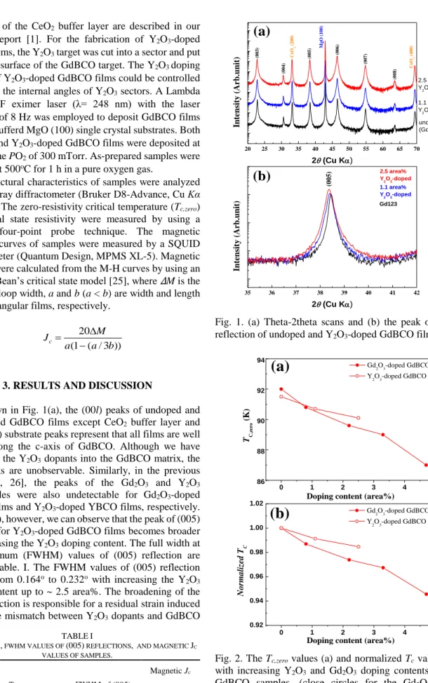
As shown in Fig. 1(a), the (00l) peaks of undoped and Y2O3-doped GdBCO films except CeO2 buffer layer and MgO (100) substrate peaks represent that all films are well aligned along the c-axis of GdBCO. Although we have introduced the Y2O3 dopants into the GdBCO matrix, the Y2O3 peaks are unobservable. Similarly, in the previous reports [1, 26], the peaks of the Gd2O3 and Y2O3
nanoparticles were also undetectable for Gd2O3-doped GdBCO films and Y2O3-doped YBCO films, respectively.
In Fig.1 (b), however, we can observe that the peak of (005) reflection for Y2O3-doped GdBCO films becomes broader with increasing the Y2O3 doping content. The full width at half maximum (FWHM) values of (005) reflection are listed in Table. I. The FWHM values of (005) reflection increase from 0.164o to 0.232o with increasing the Y2O3
doping content up to ~ 2.5 area%. The broadening of the (005) reflection is responsible for a residual strain induced by a lattice mismatch between Y2O3 dopants and GdBCO
matrix. With increasing the Y2O3 doping content, the strained area of Y2O3-doped GdBCO films will be increased, of which tendency has been reported by other
35 36 37 38 39 40 41 42
(005)
Intensity (Arb.unit)
2 (Cu K)
Gd123 1.1 area%
Y2O
3-doped 2.5 area%
Y2O3-doped
20 25 30 35 40 45 50 55 60 65 70
Intensity (Arb.unit)
2 (Cu K)
(003) (004) CeO2 (200) (005) MgO (100) (006) (007) (008) CeO2 (400)
undoped (Gd123) 1.1 area%
Y2O3-doped 2.5 area%
Y2O3-doped
(a)
(b)
Fig. 1. (a) Theta-2theta scans and (b) the peak of (005) reflection of undoped and Y2O3-doped GdBCO films.
0 1 2 3 4 5
86 88 90 92 94
TC,zero (K)
Doping content (area%)
Gd2O3-doped GdBCO Y2O3-doped GdBCO
(a)
(b)
0 1 2 3 4 5
0.92 0.94 0.96 0.98 1.00 1.02
Normalized TC
Doping content (area%)
Gd2O3-doped GdBCO Y2O3-doped GdBCO
Fig. 2. The Tc,zero values (a) and normalized Tc values (b) with increasing Y2O3 and Gd2O3 doping contents for all GdBCO samples. (close circles for the Gd2O3-doped GdBCO films from ref. [1], open circles for the Y2O3-doped GdBCO films)
TABLEI
TC,ZERO,ΔTC, FWHM VALUES OF (005) REFLECTIONS, AND MAGNETIC JC
VALUES OF SAMPLES.
Sample Tc,zero
(K) Δ Tc FWHM of (005) reflection (degree)
Magnetic Jc
@ 77 K, 0 T (MA/cm2)
Undoped 91.5 0.7 0.164 1.92
1.1 area% 90.7 0.9 0.214 1.16
2.5 area% 90.1 1.3 0.232 0.71
researchers [12, 22].
In Fig. 2(a), the Tc,zero values of samples are plotted as a function of the Y2O3 doping content. The Tc,zero values normalized to Tc,zero values of each undoped GdBCO films for Y2O3-doped and Gd2O3-doped GdBCO films are also represented in Fig. 2(b). As shown in Fig. 2(a), the Tc,zero
value of undoped sample is not exactly same with that of undoped sample of our previous report [1] probably because the samples in this study were fabricated by using another GdBCO target. The Tc,zero values for both Y2O3-doped and Gd2O3-doped GdBCO films are degraded gradually with increasing the doping content. Interestingly, however, with increasing the doping content, the Tc,zero
values of Y2O3-doped GdBCO films are less degraded compared with those of Gd2O3-doped GdBCO films, which is in good agreement with our expectation that an additional Tc drop due to the formation of the Gd1+xBa2-xCu3O7-δ -type solid solutions can be suppressed by using the Y2O3 dopant.
The field dependence of magnetic Jc values at 77, 65, 40, and 20 K, which were calculated using a modified Bean model [25], are represented in Fig. 3. In Fig. 3(a), Y2O3-doped GdBCO films exhibit a gradual degradation of self-field Jc value with increasing the Y2O3 doping content at 77 K. This tendency of self-field Jc degradation was also observable in previous reports [8, 22]. The magnetic Jc
values of undoped GdBCO films for B//c are higher than those of Y2O3-doped GdBCO films at 77 K in Fig. 3(a) while the Jc values of 1.1 area% Y2O3-doped GdBCO films are slightly higher than those of undoped GdBCO films in the magnetic fields ranging from 0.05 to 4.5 T at 65 K in Fig. 3(b). In Fig. 3(c), the 1.1 and 2.5 area% Y2O3-doped GdBCO film exhibit enhanced Jc values in the magnetic fields from 0.03 T to 4 T and from 0.3 T to 4 T at 40 K, respectively. This tendency differs from the behavior of Jc-B curves at 77 K. Unlike Gd2O3-doped GdBCO films in our previous study [1], exhibiting degraded Jc values with increasing the magnetic fields at the temperature of 65 K due to a severe Tc drop, 1.1 area% Y2O3-doped GdBCO film shows slightly improved Jc values for B//c at 65 K since the Tc drop of Y2O3-doped GdBCO films was less than that of Gd2O3-doped GdBCO films. Therefore, it is crucial to minimize the Tc degradation in order to enhance the pinning properties at relatively high temperatures when the 3D-APCs such as nanoparticles are introduced into the superconducting matrix by the PLD process.
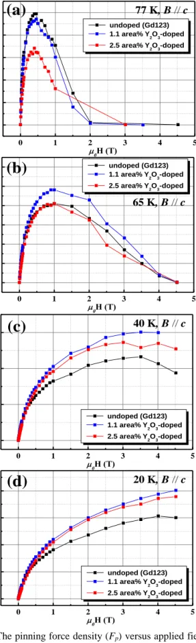
Fig.4 shows the Fp values of undoped and Y2O3-doped GdBCO films for B//c at 77, 65, 40, and 20 K. The maximum Fp values for the undoped GdBCO films are higher than those of Y2O3-doped GdBCO films for B//c at 77 K in Fig. 4(a). Among all the samples, the maximum Fp
values of 1.1 area% Y2O3-doped GdBCO film are higher than those of other samples at 65 K in Fig. 4(b). Especially, in Fig. 4(c), the 2.5 area% Y2O3-doped GdBCO film shows the enhanced Fp values at 40 K compared with undoped GdBCO films. However, the 2.2 area% Gd2O3-doped GdBCO film exhibits degraded Fp values in the magnetic fields ranging from 3.2 T to 4.8 T at 40 K compared with
the undoped GdBCO films in our previous report [1] since the Tc,zero value of 89.6 K for 2.2 area % Gd2O3-doped
0.01 0.1 1
100 101 102 103 104 105 106 107
undoped (Gd123) 1.1 area% Y
2O
3-doped 2.5 area% Y
2O
3-doped
77 K, B//c
JC (A/cm2 )
0H (T)
0.01 0.1 1
106
undoped (Gd123) 1.1 area% Y
2O
3-doped 2.5 area% Y
2O
3-doped
40 K, B//c
JC (A/cm2 )
0H (T)
0.01 0.1 1
106 107
undoped (Gd123) 1.1 area% Y
2O
3-doped 2.5 area% Y
2O
3-doped
20 K, B//c
JC (A/cm2 )
0H (T)
0.01 0.1 1
102 103 104 105 106
undoped (Gd123) 1.1 area% Y
2O
3-doped 2.5 area% Y
2O
3-doped
65 K, B//c
JC (A/cm2 )
0H (T)
(a)
(b)
(c)
(d)
Fig. 3. Field dependence of magnetic Jc for undoped and Y2O3-doped GdBCO films at (a) 77, (b) 65, (c) 40, and (d) 20 K.
GdBCO film was inferior to that of 90.1 K for 2.5 area % Y2O3-doped GdBCO film.
Although the Y2O3-doped GdBCO films have a lower Tc
drop compared with Gd2O3-doped GdBCO films, the Jc
values of Y2O3-doped GdBCO films are still lower than undoped GdBCO films for B//c at 77 K. M. Miura et al.
[27] reported that a coherent interface of PLD-films between the matrix and second phase affected the Tc and self-field Jc values at 77 K. The BHO-doped GdBCO films by PLD showed the degradation in Tc and self-field Jc
values since it has been reported that oxygen deficiency can be induced at the coherent interface region and thus it will be increased with increasing BHO doping contents up to ~ 6 vol% [27]. On the other hand, the Tc values of the BHO-doped (Y,Gd)BCO films by MOD were unaltered with increasing BHO doping contents up to ~ 12 vol%. In addition to MOD-films, the GdBCO CCs fabricated by RCE-DR exhibit the high Tc,zero value of ~ 94 K and self-field Jc values of 660 A/cm even though the GdBCO CCs have a large amount of Gd2O3 nanoparticles dispersed in the GdBCO matrix [7]. Interestingly, the Tc and self-field Jc values of samples fabricated by the MOD and RCE-DR processes are almost unaffected by the amount of a dopant.
The samples fabricated by the MOD and RCE-DR processes have an incoherent interface between the superconducting matrix and dopants due to an ex-situ annealing process where the second phases are formed before the growth of the superconducting matrix. However, the Tc and self-field Jc values of samples by the PLD process are sensitive to an amount of doping content due to the formation of a coherent interface between the second phase and the superconducting matrix, and hence leading to the serious Tc drop with increasing the doping content.
4. SUMMARY
The pinning properties of Y2O3-doped GdBCO films by the PLD process have been investigated. With increasing the Y2O3 doping content, the FWHM values of (005) reflection for Y2O3-doped GdBCO films were increased, indicating that the strain area induced by a lattice distortion might be increased. Also, the Tc,zero and ΔTc values of Y2O3-doped GdBCO films were gradually degraded with increasing the Y2O3 doping content up to 2.5 area%.
Interestingly, the Y2O3-doped GdBCO films exhibited the less Tc drop compared with Gd2O3-doped GdBCO films.
The 1.1 area% Y2O3-doped GdBCO films show slightly improved magnetic Jc and maximum Fp for B//c at relatively high temperature of 65 K compared with undoped GdBCO films. Below 40K, all Y2O3-doped GdBCO films show improved pinning properties for B//c compared with undoped sample. Consequently, the Y2O3
dopants for PLD-GdBCO films turn out to be effective for the improvement of the pinning properties at relatively low temperatures while the pinning properties of Y2O3-doped GdBCO films was improved insignificantly at relatively high temperatures.
ACKNOWLEDGMENT
This work was supported by the Korea Institute of
0 1 2 3 4 5
0.0 0.2 0.4 0.6 0.8 1.0
undoped (Gd123) 1.1 area% Y
2O
3-doped 2.5 area% Y
2O
3-doped
FP (GN/m3 )
0H (T)
77 K, B // c
0 1 2 3 4 5
0 1 2 3 4 5
6 undoped (Gd123)
1.1 area% Y
2O
3-doped 2.5 area% Y
2O
3-doped
F P (GN/m3 )
0H (T)
65 K, B // c
0 1 2 3 4 5
0 10 20 30
undoped (Gd123) 1.1 area% Y
2O
3-doped 2.5 area% Y
2O
3-doped
FP (GN/m3 )
0H (T)
40 K, B // c
0 1 2 3 4 5
0 20 40 60 80
undoped (Gd123) 1.1 area% Y
2O
3-doped 2.5 area% Y
2O
3-doped
FP (GN/m3 )
0H (T)
20 K, B // c
(a)
(b)
(c)
(d)
Fig. 4. The pinning force density (Fp) versus applied field for undoped and Y2O3-doped GdBCO films at (a) 77, (b) 65, (c) 40, and (d) 20 K.
Energy Technology Evaluation and Planning (KETEP) and the Ministry of Trade, Industry & Energy (MOTIE) of the Republic of Korea (No. 20131010501800). And, part of this study has been performed using facilities at IBS Center for Correlated Electron Systems, Seoul National University
REFERENCES
[1] W. Oh, J. Kim, and S. Yoo, “Enhanced pinning properties of GdBa2Cu3O7-δ films with the Gd2O3 nanoparticles”, IEEE Trans.
Appl. Supercond., vol. 27, p. 8000605, Jan. 2017.
[2] S. R. Foltyn, L. Civale, J. L. Macmanus-driscoll, Q. X. Jia, B.
Maiorov, H. Wang, and M. Maley, “Materials science challenges for high-temperature superconducting wire”, Nat. Mater., vol. 6, pp.
631-642, Sep. 2007
[3] K. Matsumoto, and P. Mele, “Artificial pinning center technology to enhance vortex pinning in YBCO coated conductors”, Supercond.
Sci. Technol., vol. 23, p.014001, Dec. 2009
[4] H. Kutami, T. Hayashida, S. Hanyu, C. Tashita, M. Igarashi, H. Fuji, Y. Hanada, K. Kakimoto, Y. Iijima, and T. Saitoh, “Progress in research and development on long length coated conductors in Fujikura”, Physica C, vol. 469, pp. 1290-1293, May. 2009 [5] M. Rupich, X. Li, C. Thieme, S. sathyamurthy, S. Fleshler, D.
Tucker, E. Thompson, J. Schreiber, J. Lynch, D. Buczek, K.
Demoranville, J. Inch, P. Cedrone, and J. Slack, “Advances in second generation high temperature superconducting wire manufacturing and R&D at American Superconductor Corporation”, Supercond. Sci. Technol., vol. 23, p. 014015, Dec.
2009
[6] V. Selvamanickam, Y. Chen, X. Xiong, Y. Xie, M. Martchevski, A.
Rar, Y. Qiao, R. Schmidt, A. Knoll, K. Lenseth, and C. Weber,
“High performance 2G wires: From R&D to pilot-scale manufacturing”, IEEE Trans. Appl. Supercond., vol. 19, no. 3, pp.
3225-3230, Jul. 2009
[7] J. H. Lee, H. Lee, J. W. Lee, S. M. Choi, S. I. Yoo, and S. H. Moon,
“RCE-DR, a novel process for coated conductor fabrication with high performance”, Supercond. Sci. Technol., vol. 27, pp. 044018, Mar. 2014
[8] J. L. Macmanus-driscoll, S. R. Foltyn, Q. X. Jia, H. Wang, A.
Serquis, L Civale, B. Maiorov, M. E. Hawley, M. P. Maley, and, D.
E. Peterson, “Strongly enhanced current densities in superconducting coated conductors of YBa2Cu3O7-x + BaZrO3”, Nat. Mater., vol. 3, pp. 439-443, May. 2004
[9] A. Goyal, S. Kang, K. J. Leonard, P. M. Martin, A. A. Gapud, M.
Varela, M. Paranthaman, A. O. Ijaduola, E. D. Dpecht, J. R.
Thompson, D. K. Christen, S. J. Pennycook, and F. A. List,
“Irradiation-free, columnar defects comprised of self-assembled nanodots and nanorods resulting in strongly enhanced flux-pinning in YBa2Cu3O7-δ films”, Supercond. Sci. Technol., vol. 18, pp.1533-1538, Oct. 2005
[10] Y. Yamada, K. Takahashi, H. Kobayashi, M. Konishi, T. Watanabe, A. Ibi, T. Muroga, and S. Miyata, T. Kato, T. Hirayama, and Y.
Shiohara, “Epitaxial nanostructure and defects effective for pinning in Y(RE)Ba2Cu3O7-x coated cnoductors”, Appl. Phys. Lett., vol. 87, p.132502, Sep. 2005
[11] P. Mele, K. Matsumoto, T. Horide, A. Ichinose, M. Mukaida, Y.
Yoshida, S. Horii, and R. Kita, “Ultra-high flux pinning properties of BaMO3-doped YBa2Cu3O7-x thin films”, Supercond. Sci.
Technol., vol. 21, p.032002, Feb. 2008
[12] M. Peurla, P. Paturi, Y. P. Stepanov, H. Huhtinen, Y. Y. Tse, A. C.
Bodi, J. Raittila, and R. Laiho, “Optimization of the BaZrO3 concentration in YBCO films prepared by pulsed laser deposition”, Supercond. Sci. Technol, vol. 19, pp. 767-771, Jun. 2006 [13] K. Takahashi, H. Kobayashi, Y. Yamada, A. Ibi, H. Fukushima, M.
Konishi, S. Miyata, Y. Shiohara, T. Kato, and T. Hirayama,
“Investigation of thick PLD-GdBCO and ZrO2 doped GdBCO coated conductors with high ritical current on PLD-CeO2 capped IBAD-GZO substrate tapes”, Supercond. Sci. Technol., vol. 19, no.
9, pp. 924-929, Jul. 2006.
[14] K. Schlesier, H. Huhtinen, P. Paturi, Y. P. Stepanov, and R. Laiho.,
“Structural and Superconducting Properties of undoped and BZO-doped GdBCO thin films”, IEEE Trans. Appl. Supercond., vol. 19, no. 3, pp.3407-3411, Jun. 2009.
[15] S. Lee, N. Chikumoto, T. Yokoyama, T. Machi, K. Nakao, and K.
Tanabe., “Development of In-Plume Pulsed Laser Deposition of high-Ic GdBCO films for coated conductors”, IEEE Trans. Appl.
Supercond., vol. 19, no. 3, pp.3192-3195, Jun. 2009.
[16] K. Kaneko, K. Furuya, K.Yamada, S. Sadayama, J. S. Barnard, P. A.
Midgley, T. Kato, T. Hirayama, M. Kiuchi, T. Matsushita, A. Ibi, Y.
Yamada, T. Izumi, and Y. Shiohara, “Three-dimensional analysis of BaZrO3 pinning centers gives isotropic superconductivity in GdBCO”, J. Appl. Phys., vol. 108, pp. 063901, Sep. 2010.
[17] K. Ko, S. Choi, J. Lee, R. Ko, S. Moon, C. Park, and S. Yoo,
“Optimization of the BaSnO3 Doping Content in GdBCO coated conductors by pulsed laser deposition”, IEEE Trans. Appl.
Supercond., vol. 24, no. 6, pp. 6600908, Dec. 2014.
[18] H. Tobita, K. Notoh, K. Higashikawa, M. Inoue, T. Kiss, T. Kato, T.
Hirayama, M. Yoshizumi, T. Izumi, and Y. Shiohara, “Fabrication of BaHfO3 doped GdBa2Cu3O7−δ coated conductors with the high Ic
of 85 A/cm-w under 3T at liquid nitrogen temperature (77K)”, Supercond. Sci. Technol., vol. 25, no. 6, pp. 062002, May. 2012.
[19] T. Matsushita, H. Nagamizu, K. Tanabe, M. Kiuchi, E.S. Otabe, H.
Tobita, M. Yoshizumi, T. Izumi, Y. Shiohara, D. Yokoe, T. Kato, and T. Hirayama, “Improvement of flux pinning performance at high magnetic fields in GdBCO coated conductors with BHO nano-rods through enhancement of Bc2”, Supercond. Sci. Technol, vol. 25, no. 12, pp. 125003, Oct. 2012.
[20] T. Yoshida, A. Ibi, T. Takahashi, M. Yoshizumi, T. Izumi, and Y.
Shiohara, “Fabrication of Eu1Ba2Cu3O7-δ + BaHfO3 coated conductors with 141 A/cm-w under 3 T at 77 K using the IBAD/PLD process”, Physica C., vol. 504, pp. 42-46, Apr. 2014 [21] A. A. Gapud, D. Kumar, S. K. Viswanathan, C. Cantoni, M. Varela,
J. Abiade, S. J. Pennycook, and D. K. Christen, “Enhancement of flux pinning in YBa2Cu3O7-δ thin films embedded with epitaxially grown Y2O3 nanostructures using a multi-layering process”, Supercond. Sci. Technol, vol. 18, pp. 1502-1505, Oct. 2005 [22] M. Malmivirta, L. D. Yao, S. Inkinen, H. Huhtinen, H. Palonen, R.
Jha, V. P. S. Awana, S. van Dijken, and P. Paturi, “The angular dependence of the critical current of BaCeO3 doped YBa2Cu3O6+x
thin films, IEEE Trans. Appl. Supercond., vol. 25, no. 3, p.6603305, Jun. 2015
[23] P. Mele, R. Guzman, J. Gazquez, T. Puig, X. Obradors, S. Saini, Y.
yoshida, M. Mukaida, A. Ichinose, K. Matsumoto, and M. I. Adam,
“High pinning performance of YBa2Cu3O7-x films added with Y2O3
nanoparticulate defects”, Supercond. Sci. Technol, vol. 28, p.
024002, Dec. 2014
[24] K. Zhang, B. Dabrowski, C. U. Segre, D. G. Hinks, I. K. Schuller, J.
D. Jorgensen, and M. Slaski, “Solubility and superconductivity in RE(Ba2-xREx)Cu3O7+δ systems (RE = Nd, Sm, Eu, Gd, Dy)”, J.
Phys. C: Solid state Phys., vol. 20, pp. L935-L940, 1987 [25] E.M. Gyorgy, R.B. van Dover, K.A. Jackson, L.F. Schneemeyer,
and J.V. Waszczak, “Anisotropic critical currents in Ba2YCu3O7
analyzed using an extended bean model”, Appl. Phys. Lett., vol. 55, pp.283, May. 1989
[26] P. Mele, M. I. Adam, T. Suzuki, Y. Yoshida, S. Awaji, A. Ichinose, S. Saini, A. K. Jha, and K. Matsumoto, “Effect of simultaneous addition of 1D and 3D artificial pinning centers in hybrid YBa2Cu3O7-x multilayers”, Sci. Adv. Mater., vol. 9, pp.1042-1050, Jun. 2017
[27] M. Miura, B. Maiorov, M. Sato, M. Kanai, T. Kato, T. Kato, T.
Izumi, S. Awaji, P. Mele, M. Kiuchi, and T. Matsushita, “Tuning nanoparticle size for enhanced functionality in perovskite thin films deposited by metal organic deposition”, NPG. Asia. Mater., vol.9, p.
e447, Sep. 2017