http://dx.doi.org/10.6111/JKCGCT.2013.23.5.224
Optical properties of vanadium dioxide thin films on c-Al
2O
3(001) sub- strates by in-situ RF magnetron sputtering
Seung Ho Han*, So Hee Kang*
,**, Hyeongkeun Kim*, Dae Ho Yoon** and Woo Seok Yang*
,†*Electronic Materials & Device Research Center, Korea Electronics Technology Institute, Seongnam, Gyeonggi 463-816, Korea
**School of Advanced Materials Science and Engineering, Sungkyunkwan University, Suwon 440-746, Korea (Received September 2, 2013)
(Revised October 8, 2013) (Accepted October 18, 2013)
Abstract Vanadium oxide thin films were deposited on c-Al2O3 (001) substrate by in-situ RF magnetron sputtering.
Oxygen partial pressure was adjusted to prepare thermochromic VO2 phase. X-ray diffraction patterns and scanning electron microscopy convincingly showed that plate-like V2O5 grains were changed into round-shape VO2 grains as oxygen partial pressure decreased. After the optimized deposition conditions were fixed, the effect of substrate temperature and orientation on the optical properties of VO2 thin films was analyzed.
Key words VO2, Thermochromic, Optical properties, Crystal structure, Microstructure, Thin Films
1. Introduction
Thermochromic materials are capable of reversible change of their optical properties in response to temper- ature [1]. Such materials have been attracting great attention in applications including smart window coat- ings for buildings and vehicles to control the solar irradi- ance automatically. Vanadium oxide (VO
2) is a promising candidate for thermochromic application. The crystal exhibits an abrupt metal-insulator transition at a critical temperature T
C= 68
oC [2,3]. The metal-insulator transi- tion of VO
2is attributed to crystallographic structure change, which is from monoclinic to tetragonal. Below T
C, the material is semiconducting and IR transparent;
above T
C, it is metallic and IR reflecting.
There have been many reports for the fabrication of VO
2by pulsed laser deposition [4-6], sol-gel process [7, 8], atmospheric pressure chemical vapor deposition [9, 10], and magnetron sputtering [11-13]. Among them, magnetron sputtering method has advantages for high deposition rate and large area deposition. However, dep- osition of VO
2thin films by magnetron sputtering has been quite difficult due to the very narrow phase exist- ence in the complex V-O system [14, 15]. To form a single phase VO
2thin film by reactive magnetron sput- tering, oxygen partial pressure should be precisely con- trolled. While many studies have reported VO
2films by
magnetron sputtering methods, few studies have been focused on the effect of crystal structure and microstruc- ture change on the optical properties of VO
2thin films [15, 16]. In particular, optical properties of VO
2thin films on c-Al
2O
3(001) substrate have been scarcely reported [11].
In the current study, thermochromic vanadium oxide thin films were deposited on c-Al
2O
3(001) substrates by
in-situ RF magnetron sputtering. Optimum depositionconditions to prepare highly oriented VO
2thin film were found with changing oxygen partial pressure (P
O). The effect of substrate temperature (T
S) and orientation on the crystal structure, microstructure, optical transmittance, and transition behavior of VO
2thin films was analyzed.
2. Research Procedure 2.1. Films Preparation
The c-Al
2O
3(001) single crystal substrates were ultra- sonically cleaned with acetone, absolute methyl alco- hol, and de-ionized water for 5 minutes, respectively.
The VO
2thin films were deposited on c-cut sapphire substrates by reactive radio frequency (RF) magnetron sputtering using a V metal target of 2 inch in diameter with 99.9 % purity. The RF power, total flow rate, and working pressure were maintained at 150 W, 50 sccm, and 30 mTorr, respectively during the deposition. The P
Owas changed from 0.8 to 1.1 sccm (1.6 to 2.2 %) to find the optimum condition for obtaining VO
2thin film.
†Corresponding author
†Tel: +82-31-789-7256
†Fax: +82-31-789-7249
†E-mail: [email protected]
The mass flow controller was applied for the fine con- trol of O
2flow ratio. The T
Swas varied from 300
oC to 400
oC. The lowest T
Sto obtain crystalline VO
2was found to be 300
oC.
2.2. Characterizations
The crystal structure and phase composition of the vanadium oxide film was determined using X-ray dif- fractometry (XRD) in the θ-2θ mode with CuKα radia- tion operated at 30 kV and 20 mA in a 2 θ range of 15~
60
o. To observe the surface microstructure of VO
2thin films, scanning electron microscopy (SEM) was used.
Spectral transmittance was measured using UV-Vis spec- trometer at wavelengths between 400 to 2500 nm with a step width of 2 nm. Temperature-dependent transmittance curve (hysteresis curve) was also obtained using UV-Vis spectrometer at wavelength of 2500 nm. From the hys- teresis curve, the midpoint of heating curve (T1), mid- point of cooling curve (T2), hysteresis width (T: difference between the T1 and T2), and transmittance difference ( ∆Tr = Tr(30
o) - Tr(90
oC)) were evaluated. The T
C(min- imum of the derivative of the heating curve) was also evaluated.
3. Results and Discussion
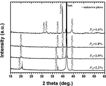
The XRD patterns of the vanadium oxide thin films deposited with oxygen partial pressures of 2.2, 2.0, 1.8, and 1.6 % are presented in Fig. 1. The thin films were
in-situ heated at TSof 400
oC. It can be seen that the intensity of the VO
2(020) is gradually increased whereas
the intensity of the V
2O
5(410) phase is gradually decreased as the P
Odecreased from 2.2 to 1.6 %. Although V
2O
5second phase and VO
2(012) plane was found in the vanadium oxide film deposited with the P
Oof 1.6 %, VO
2phase was highly oriented with (010) planes paral- lel to the surface of the substrate. For the VO
2(020) peak, the full width half maximum (FWHM) value is found to be about 0.19
o, which corresponds to high crystallinity thin film. The VO
2(010)
m//Al
2O
3(001) rela- tionship is consistent with previous reports [6, 17].
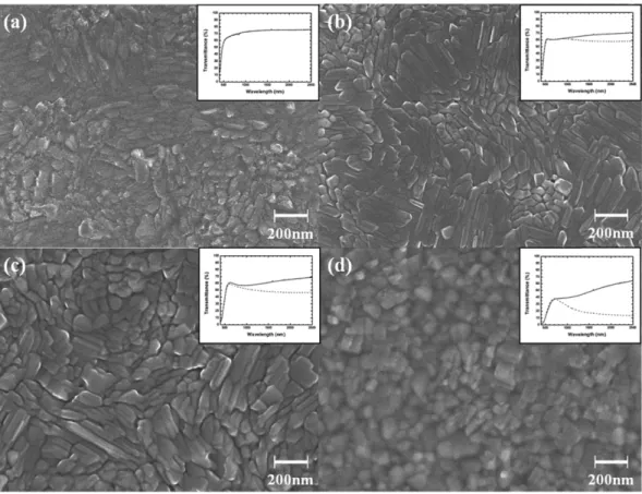
Fig. 2 shows SEM images of the vanadium oxide thin films deposited with oxygen partial pressures of 2.2 (a), 1.8 (b), 2.0 (c) and 2.2 % (d). The insets are correspond- ing spectral transmittance. As the oxygen partial pres- sure decreased the fraction of plate-like grains were reduced and round-shape grains were increased. Accord- ing to Figs. 1 and 2, it might be concluded that plate- like grains correspond to V
2O
5phase and round-shape grains correspond to VO
2phase. Spectral transmittances confirm that the thermochromic properties are enhanced as VO
2phase increases. As the V
2O
5phase is the most stable oxide in the V-O system [18-20], oxygen partial pressure should be precisely adjusted to form VO
2phase.
XRD patterns and SEM images obtained from VO
2thin films deposited at the T
Sof 300 and 350
oC with oxygen partial pressure of 1.6 % are shown in Fig. 3(a).
It can be seen that the intensity of the VO
2(020) peak decreases as the T
Sdecreases from 350 to 300
oC. Aver- age grain size of the thin films was calculated using Scherrer’s formula [21]:
where b is the average grain size, λ = 1.541 Å (X-ray wavelength), and β is the FWHM for the diffraction angle 2θ. The calculated grain sizes of the VO
2thin films deposited at the T
Sof 300 and 350
oC are 5.8 and 6.8 nm, respectively. SEM images also follow a similar trend to the calculated grain sizes. Both images show uniform-sized nano-grain but the VO
2thin films depos- ited at 350
oC have relatively large grain sizes than the VO
2thin films deposited at 300
oC. In order to investi- gate the influence of T
Son the crystal structure, we obtained subtle XRD patterns of 2θ near 39.8, as shown in Fig. 3(b). As T
Sincreases from 300 to 350
oC, the dif- fraction peak of VO
2(020) shift to higher position from 39.84 to 39.92, which correspond to (010) lattice spac- ing of 4.523 Å and 4.514 Å, respectively. Epitaxial VO
2thin film deposited on c-Al
2O
3(001) substrate with T
Sof 400
oC showed VO
2(020) position of 2 θ = 39.98 −
b = 0.9λ β cos θ ---
Fig. 1. XRD patterns of the vanadium oxide thin films deposited with oxygen partial pressures of 2.2, 2.0, 1.8, and 1.6 %.
40.0 [6, 17], indicating that our VO
2thin film deposited at the T
Sof 350
oC have similar crystal structure with epitaxial thin film with good crystallinity but the VO
2thin film deposited at the T
Sof 300
oC is not fully crys- tallized and have relatively open structures.
Fig. 4 shows the spectral transmittance of the VO
2thin films deposited at 300
oC (a) and 350
oC (b) at T <
T
C(30
oC) and T > T
C(90
oC). The film deposited at 350
oC shows higher visible region transmittance and Tr than the film deposited at 300
oC due to larger grain size and better crystallinity. However, both films show large trans- mittance difference between the semiconductor state of
Fig. 3. (a) XRD patterns and SEM images of VO2 thin films deposited at the TS of 300 and 350oC with oxygen partial pressure of1.6 % and (b) subtle XRD patterns of 2θ near 39.8o.
Fig. 2. SEM images of the vanadium oxide thin films deposited with oxygen partial pressures of 2.2 (a), 2.0 (b), 1.8 (c), and 1.6 % (d).
The insets are corresponding spectral transmittance.
T < T
C(30
oC) and metal state of T > T
C(90
oC) in the infrared region, which means good thermochromic property.
Hysteresis curves of the VO
2thin films deposited at 300
oC (a) and 350
oC (b) are shown in Fig. 5. Table 1 shows the T1, T2, T, Tr, and the T
Cof the VO
2thin films deposited at 300
oC and 350
oC in which obtained from Fig. 5. While the VO
2thin film deposited at 350
oC have relatively sharp decrease of transmittance with Tr of 55.4 %, the film deposited at 300
oC have broad change of transmittance with decreased Tr of 45.8 %.
The T is increased from 9.6 to 11.4
oC and the T
Cis decreased from 77.5 to 70.3
oC with decreasing T
S. The VO
2films deposited at low temperature can lead to the destabilization of low-temperature semiconductor phase
and thereby causing reduced T
Cand transition sharp- ness [15, 22], which is consistent with our results. How- ever, considering the reduced T
Cby the crystalline imperfection, the T
Cof the both films are still larger than the bulk value of ~68
oC.
The lattice parameters and thermal expansion coeffi- cients for the rhombohedral Al
2O
3substrate and mono- clinic VO
2film are shown in Table 2. The lattice parameter a of rhombohedral Al
2O
3is 4.758 and the lattice param- eters a, b and c of monoclinic VO
2are 5.753, 4.526, and 5.382, respectively. The epitaxial VO
2(010)//Al
2O
3(001) can induce the epitaxial relationship of VO
2(010)//Al
2O
3(001),
Fig. 4. Spectral transmittance of the VO2 thin films depositedat 300oC (a) and 350oC (b) at T < TC (30oC) and T > TC (90oC).
Fig. 5. Temperature-dependent transmittance curve (hysteresis curve) of the VO2 thin films deposited at (a) 300oC and (b)
350oC.
Table 1
The T1, T2, ∆Tr, ∆T, and the TC of the VO2 thin films deposited at 300 and 350oC
TS ∆Tr (%) T1 (oC) T2 (oC) ∆T (oC) TC (oC)
300oC 45.8 69.2 57.8 11.4 70.3
350oC 55.4 72.0 63.2 8.8 72.5
Table 2
Lattice parameters of rhombohedral Al2O3 substrate and monoclinic VO2 film
Materials Lattice parameters (Å)
a c
Al2O3 4.758 12.992
VO2 a = 5.753, b = 4.526 5.382
(100)//(100). As a result, in-plane compressive stress and corresponding out of plane tensile stress can be induced.
In the form of thin film, the T
Cof VO
2can be modified by the control of c-axis stress induced by the lattice mismatch between the film and substrate [5,23]. The c- axis compressive stress decreases the T
C, whereas the c- axis tensile stress increases the T
C. The increased T
Cof our VO
2thin film deposited on c-Al
2O
3(001) might be originated from increased c-axis tensile stress.
As mentioned earlier, the lattice spacing was decreased from 4.523 Å to 4.514 Å with increasing T
Sfrom 300 to 350
oC. The decrease in c-axis lattice spacing means
c-axis compressive stress, and hence the TCshould be decreased. However, the T
Cwas increased with great extent of ~7.2
oC with increasing T
Sfrom 300 to 350
oC, that is opposite tendency compared with previous reports [5, 23]. A more detailed research concerning the correlation between the T
Sand the T
Cof the VO
2films deposited on c-Al
2O
3(001) substrate is under investigation.
4. Conclusions
Vanadium oxide thin films were deposited on c-Al
2O
3(001) substrate by in-situ RF magnetron sputtering. As the oxygen partial pressure decreased, rod-like V
2O
5grains were reduced and plate-like VO
2grains were increased.
With increasing substrate temperature, grain size increased and (010) lattice spacing decreased from 4.52 to 4.514 Å.
The VO
2thin films deposited at 300 and 350
oC showed large transmittance difference between the semiconduc- tor state and metal state in the infrared region, which implies good thermochromic property. While the VO
2thin film deposited at 350
oC had relatively sharp decrease of transmittance, the film deposited at 300
oC had broad change of transmittance with decreased Tr due to the crystalline imperfection. The increase in T
Cof VO
2thin film deposited on c-Al
2O
3(001) substrate compared with bulk VO
2might be originated from c-axis tensile stress induced by lattice mismatch.
Acknowledgement
This work was supported by Technology Innovation Program (No. 10044410, Commercialization of flexible touch panels based on 900x1600 mm
2large, less than 1 nm thick graphene film synthesis technique) funded by the Ministry of Trade, Industry.
References
[ 1 ] C.G. Granqvist, “Materials science for solar energy con- version systems”, (Pergamon Press, Oxford, 1991) Chap. 5.
[ 2 ] F.J. Morin, “Oxides which show a metal-to-insulator transition at the Neel temperature”, Phys. Rev. Lett. 3 (1959) 34.
[ 3 ] J.B. Goodenough, “The two compounds of the crystallo- graphic transition in VO2”, J. Solid State Chem. 3 (1971) 490.
[ 4 ] D.H. Kim and H.S. Kwok, “Pulsed laser deposition of VO2 thin films”, Appl. Phys. Lett. 65 (1994) 3188.
[ 5 ] Y. Muraoka and Z. Hiroi, “Metal-insulator transition of VO2 thin films grown on TiO2 (001) and (110) sub- strates”, Appl. Phys. Lett. 80 (2002) 583.
[ 6 ] K. Okimura, J. Sakai and S. Ramanathan, “In situ x-ray diffraction studies on epitaxial VO2 films grown on c- Al2O3 during thermally induced insulator-metal transi- tion”, J. Appl. Phys. 107 (2010) 063503.
[ 7 ] H.-T. Kim, Y.W. Lee, B.-J. Kim, B.-G. Chae, S.J. Yun, K.-Y. Kang, K.-J. Han, K.-J. Yee and Y.-S. Lim, “Mon- oclinic and correlated metal phase in VO2 as evidence of the Mott transition: coherent phonon analysis”, Phys.
Rev. Lett. 97 (2006) 266401.
[ 8 ] B.-J. Kim, Y.W. Lee, B.-G. Chae, S.J. Yun, S.-Y. Oh and H.-T. Kim, “Temperature dependence of the first-order metal-insulator transition in VO2 and programmable criti- cal temperature sensor”, Appl. Phys. Lett. 90 (2007) 023515.
[ 9 ] U. Qureshi, T.D. Manning and I.P. Parkin, “Atmo- spheric pressure chemical vapour deposition of VO2 and VO2/TiO2 films from the reaction of VOCl3, TiCl4 and water”, J. Mater. Chem. 14 (2004) 1190.
[10] R. Binions, G. Hyett, C. Piccirillo and I.P. Parkin, “Syn- thesis and terahertz transmission properties of nano- porous vanadium dioxide films”, J. Mater. Chem. 17 (2007) 4652.
[11] G. Xu, P. Jin, M. Tazawa and K. Yoshimura, “VO2- Sb:SnO2 composite thermochromic smart glass foil”, Appl. Surf. Sci. 244 (2005) 449.
[12] H. Kakiuchida, P. Jin, S. Nakao and M. Tazawa, “Opti- cal properties of vanadium dioxide film during semicon- ductive-metallic phase transition”, Jpn. J. Appl. Phys. 46 (2007) L113.
[13] Z. Yang and S. Ramanathan, “Direct measurement of compositional complexity-induced electronic inhomoge- neity in VO2 thin films grown on gate dielectrics”, Appl. Phys. Lett. 98 (2011) 192113.
[14] C.H. Griffiths and H.K. Eastwood, “Influence on sto- ichiometry on the metal-semiconductor transition in vanadium dioxide”, J. Appl. Phys. 45 (1974) 2201.
[15] P. Jin, K. Yoshimura and S. Tanemura, “Dependence of microstructure and thermochromism on substrate tem- perature for sputter-deposited VO2 epitaxial films”, J.
Vac. Sci. Technol. A. 15 [3] (1997) 1113.
[16] J. Lappalainen, S. Heinilehto, S. Saukko, V. Lantto and H. Jantunen, “Microstructure dependent switching prop- erties of VO2 thin films”, Sens. Actuators A 142 (2008) 250.
[17] K. Okimura and Y. Suzuki, “Epitaxial growth of V2O3
thin films on c-plane Al2O3 in reactive sputtering and its transformation to VO2 films by post annealing”, Jpn. J.
Appl. Phys. 50 (2011) 065803.
[18] C.W. Zou, X.D. Yan, D.A. Patterson, E.A.C. Emanuels- son, J.M. Bian and W. Gao, “Temperature sensitive crystallization of V2O5: from amorphous film to β-V2O5 nanorods”, Cryst. Eng. Comm. 12 (2010) 691.
[19] N. Fateh, G.A. Fontalvo, L. Cha, T. Klünsner, G. Hla- wacek, C. Teichert and C. Mitterer, “Synthesis-structure relations for reactive magnetron sputtered V2O5 films”, Surf. Coat. Technol. 202 (2008) 1551.
[20] P. Singh and D. Kaur, “Influence of film thickness on texture and electrical and optical properties of room
temperature deposited nanocrystalline V2O5 thin films”, J. Appl. Phys. 103 (2008) 043507.
[21] B.D. Cullity, “Elements of X-ray diffraction” (Addison- Wesley, Reading, MA, 1978).
[22] Y. Muraoka, Y. Ueda and Z. Hiroi, “Large modification of the metal-insulator transition temperature in strained VO2 films grown on TiO2 substrates”, J. Phys. Chem.
Solids 63 (2002) 965.
[23] L.A. Ladd and W. Paul, “Optical and transport proper- ties of high quality crystals of V2O4 near the metallic transition temperature”, Solid State Commun. 7 (1969) 425.