P1-87 / D. Y. Yoon
• IMID 2009 DIGEST
Abstract
We have investigated the effect of host on the device charactistics of green phosphorescent organic light emitting devices consising of mCP ,CBP and TPBi. Electrons were confined within the device by inserting hole transport layer between the electro transport and the emitting layer. When the appropriate interlayers were added, the device with TPBI host layer performances were found to be dramatically enhanced, with current efficiency and lifetime of 18cd/A and 18hour .
1. Introduction
Electroluminescent (EL) devices based on organic thin films are one of the most promising next-generation low-cost full-color flat panel displays alternative to liquid crystal-based ones. Recently phosphorescent organic light-emitting devices (PHOLEDs) have received considerable attention due to the ability of highly efficient emission compared with conventional fluorescent OLEDs.[1–5] However, the external quantum efficiency (photons extracted in the forward direction per electron injected)[6,7] is not enough to reach the theoretical limit of about 20% derived from simple classical optics, although very recently there were a few reports concerning the external quantum efficiencies of close to or greater than 20% only at low injection current densities below 0.1 mA/cm[2.8,9] In simple-matrix (dot-matrix) EL displays, the devices instantaneously require high luminance for the high duty drive. Consequently, high injection current is required to generate high luminance. If we employ the PHOLEDs for such displays, we can reduce the injection current
compared with fluorescent OLEDs, leading to the prevention of degradation of the devices.
2. Experimental
The ITO substrates were sonicated in distilled water for 5 min and in isopropyl alcohol for an additional 5 min to remove particles and organic contaminants on ITO glasses. The ITO glasses were further treated with boiled isopropyl alcohol for additional cleaning. After cleaning, the ITO substrates were surface treated with O2 plasma for 5 min to control the work function
of ITO. The ITO substrates were transferred the glove box the vacuum chamber for organic materials and metal deposition.
A series of organic light-emitting diodes were fabricated with the structure of indium tin oxide (ITO)/2-TNATA (35nm)/NPB(25nm)/EML (30nm)/ BCP(5nm)/Bebq2(30nm)/LiF(0.5nm)/Al(120nm).
4,4’,4’’-tris[N-2-naphthyl]-N-phenyl-amino]triphenyl amine (2-TNATA), 4,4’-bis[N-(1-nathyl)-Nphenyl amino] biphenyl] (NPB), and Bathocuproine(BCP) , bis(10-hydroxybenzo[h] qinolinato) beryllium(Bebq2)
were as the hole injecton layer(HIL), the hole transporting layer(HTL), hole blocking layer(HBL), electron transporting layer(ETL), respectively. fac-tris(2-phenylpyridine)iridium Ir(ppy)3 was doped into
host 4,48-N,N8-dicarbazole-biphenyl (CBP), 3,58-N,N8 -dicarbazole-benzene (mCP) and TPBI.
All organic materials except for dopant material were at a deposition rate of 2Å/s and Al was evaporated at a rate of 1~2 Å/s. The spectrum and brightness of the fabricated devices was measured by a Minolta CS-1000 spectroradi-ometer. The current density - voltage (I-V) characteristics of the green
Influence of green phosphorescent organic light-emitting
devices of host by hole transport layer
Do-Yeol Yoon1)2), Chan-Jae Lee1), Dae-Gyu Moon2), Jeong-No Lee1)
1) Display Components & Material Research Center, Korea Electronics Technology Institute, #68, Yatap, Seoungnam, Gyeonggi-do, 463-816, Korea 2) Department of Materials Engineering, Soonchunhyang University, 646,
Eupnae-ri, Shinchang-myeon, Asan-si, Chungcheongnam–do, Korea Phone: 011-9039-9083 , E-mail:[email protected]
P1-87 / D. Y. Yoon
IMID 2009 DIGEST • PHOLEDs were measured by a Keithley 2400 source
meter and calibrated photodiode.
Fig. 1 shows the schematic structures of the fabricated devices
3. Results and discussion
400 450 500 550 600 650 700 750 0.0 0.2 0.4 0.6 0.8 1.0 EL Inte ns ity (a. u.) Wave length(nm) CBP mCP TPBi
Fig.2 EL spectra of the devices with different host matrials
Fig. 2 shows the EL spectrum of devices. All the devices exhibit a similar maximum luminescence wavelength, near 516 nm, which originates from the triplet emission of Ir(ppy)3, while host CBP device, host mCP and host TPBI device with a NPD interlayer exhibit another broad shoulder near 450 nm that is due to NPB emission. The result indicates that the emission is entirely due to EML and NPD
0 2 4 6 8 10 12 14 0 100 200 300 400 Cur rent de nsity(m A /cm 2 ) Voltage(V) CBP mCP TPBi
Fig. 3 I-V characteristics of the devices with different host materials.
.
Fig. 3 shows I-V of devices with CBP, mCP, TPBi host layers. The highest current density could be obtained in TPBI host device, while CBP host device showed the lowest current density. Because TPBI electron mobility is more rapid than in devices with CBP, mCP host layers 0 50 100 150 200 250 300 350 400 0 4 8 12 16 20 C ur re nt e ffi cie ncy( cd /A ) Current density(mA/cm2 ) CBP mCP TPBi
Fig. 4 Current efficiency characteristics
Fig. 4 shows the current efficiency-current density curves for the devices. The CBP device and mCP device shows the current efficiency of 9.6 cd/A and 4.6 cd/A, but TPBi device shows the current efficiency of 18 cd/A. Because TPBI current density and electron mobility is more high than CBP, mCP host layers. Therefore recombination position is change NPD(2nm) CBP:Ir(ppy)3 (10%,30nm) ITO Bebq2 (10nm) 2T-NATA (20nm) NPD(25nm) Glass LiF(0.5nm) Al(120nm)
Device A Device B Device C
NPD(2nm) mCP:Ir(ppy)3 (10%,30nm) ITO Bebq2 (10nm) 2T-NATA (20nm) NPD(25nm) Glass LiF(0.5nm) Al(120nm) NPD(2nm) TPBi:Ir(ppy)3 (10%,30nm) ITO Bebq2 (10nm) 2T-NATA (20nm) NPD(25nm) Glass LiF(0.5nm) Al(120nm)
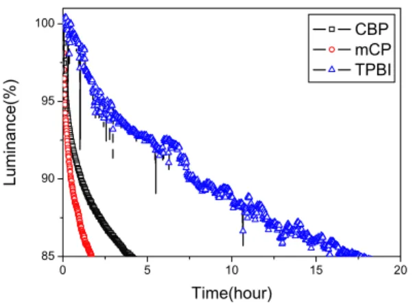
P1-87 / D. Y. Yoon • IMID 2009 DIGEST 0 5 10 15 20 85 90 95 100 Lum in a nce( % ) Time(hour) CBP mCP TPBI
Fig 5. Lifetime of the devices at 1000cd/m2
Fig 5. shows the luminance degradation as a function of operating time. The initial luminance was 1000 cd/m2. The device 85% luminance life time of
the of the device using TPBI was more than 9 time as long as that of mCP, and reached 18 hours.
4. Summary
In this study, We have investigated the effect of host on the device charactistics of green phosphorescent organic light emitting devices consising of mCP ,CBP and TPBi.
All the devices show a strongest EL intensity peak at 516, 520nm. CBP and mCP devices show a poor EL intensity peak at 450nm But TPBi devices exhibited 430nm. The device with CBP, mCP, TPBi host layer were the current efficiency of 9.6 cd/A, 4.6 cd/A and 18cd/A. The device 85% luminance life time of the of the device using TPBI was more than 9 time as long as that of mCP, and reached 18 hours
5. References
1. M. A. Baldo, D. F. O’Brien, Y. You, A. Shoustikov, S. Sibley, M. E. Thompson, and S. R. Forrest, Nature (London) 395, 151 (1998).
2. C. Adachi, M. A. Baldo, S. R. Forrest, and M. E. Thompson, Appl. Phys. Lett. 77, 904 (2000). 3. D. F. O’Brien, M. A. Baldo, M. E. Thompson,
and S. R. Forrest, Appl. Phys. Lett. 74, 442 (1999).
4. M. A. Baldo, S. Lamansky, P. E. Burrows, M. E. Thompson, and S. R. Forrest, Appl. Phys. Lett. 75, 4 (1999).
5. M. A. Baldo, M. E. Thompson, and S. R. Forrest, Nature (London) 403, 750 (2000).
6. T. Tsutsui and S. Saito, in Intrinsically Conducting Polymers: An Emerging Technology, edited by M. Aldissi (Kluwer Academic, Dordrecht), Vol. 246, p. 123 (1993)
7. L. J. Rothberg and A. J. Lovinger, J. Mater. Res. 11, 3174 (1996).
8. M.-J. Yang and T. Tsutsui, Proceedings of the 10th International Workshop on Inorganic and Organic Electroluminescence, 4–7 December, Hamamatsu, Japan, pp. 227–230. (2000)
9. A. Fukase and J. Kido, Proceedings of the 10th International Workshop on Inorganic and Organic Electroluminescence, 4–7 December, Hamamatsu, Japan, pp. 293–295. (2000)