http://dx.doi.org/10.7236/IJASC.2021.10.1.12
A Differential Voltage-controlled Oscillator as a Single-balanced Mixer
Nam-Jin Oh
Professor, Department of Electronic Engineering, Korea National University of Transportation,
Korea
E-mail : [email protected]
Abstract
This paper proposes a low power radio frequency receiver front-end where, in a single stage, single-balanced mixer and voltage-controlled oscillator are stacked on top of low noise amplifier and re-use the dc current to reduce the power consumption. In the proposed topology, the voltage-controlled oscillator itself plays the dual role of oscillator and mixer by exploiting a series inductor-capacitor network. Using a 65 nm complementary metal oxide semiconductor technology, the proposed radio frequency front-end is designed and simulated. Oscillating at around 2.4 GHz frequency band, the voltage-controlled oscillator of the proposed radio frequency front-end achieves the phase noise of ‒72 dBc/Hz, ‒93 dBc/Hz, and ‒113 dBc/Hz at 10KHz, 100KHz, and 1 MHz offset frequency, respectively. The simulated voltage conversion gain is about 25 dB. The double-side band noise figure is ‒14.2 dB, ‒8.8 dB, and ‒7.3 dB at 100 KHz, 1 MHz and 10 MHz offset. The radio frequency front-end consumes only 96 μW dc power from a 1-V supply.
Keywords: CMOS, Phase Noise, Single-balanced Mixer, Series LC Tank, LMV Cell, Voltage-controlled Oscillator
1. Introduction
Highly integrated, low-power, and low-voltage circuits are always the main topics for integrated circuit designers, especially very important for mobile wireless communication systems due to the limitation of battery life [1-3]. Single stage circuits combining mixer and oscillator have been designed for the purpose of a higher degree of integration and reducing power consumption. For highly integrated low-power receiver front-end, a current reuse technique has typically been chosen across different functional blocks. A popular method is cascoding the mixer on top of the input stage of a low-noise amplifier (LNA), while less frequent method is stacking mixer and voltage-controlled oscillator (VCO) [4, 5]. Figure 1 shows the several kinds of radio frequency (RF) receiver front-end using the current-reuse technique. In [4], a double balanced mixer is stacked on top of the VCO by using the current reuse topology. The RF input signal is applied to the input of the mixer, and the oscillator signal is applied to the source nodes of the mixer. Moreover, this topology applies a separate dc bias to the VCO. In [5], the RF front-end merges LNA, mixer, and VCO (LMV) in a single stage. This topology stacks VCO on top of the mixer. The current source of the mixer is modified as the LNA with inductor degeneration for LNA. This topology performs RF amplification, mixing, and local oscillator (LO)
IJASC 21-1-2
Manuscript Received: January. 15, 2021/ Revised: March. 16, 2021/ Accepted: March. 19, 2021 Corresponding Author: [email protected]
Tel: +82-43-841-5162, Fax: +82-43-841-5160
generation while sharing the same bias current and the same devices among all the blocks of the RF front-end, resulting in a very low-power and small-area chip solution. Since the intermediate frequency (IF) outputs are connected to the source nodes of the VCO, the voltage gain is limited due to the low impedance at the source nodes.
(a) (b)
(c)
Figure 1. (a) Type I LMV [4] and (b) Type II LMV [5], and (c) Type III LMV [6].
In [6], a new type of VCO as a mixer topology is proposed by modifying the complementary VCO and adopting a series inductor-capacitor LC (SLC) network. The SLC network enables to extract the IF signal component at the VCO output nodes. However, this topology has higher noise figure (NF) since it adopts a complementary topology for low power consumption. Also, it does not provide the low gain mode since the oscillation stops with the low load resistance and suffers from large variation of VCO output swing with the
load resistor RL. Furthermore, it consumes quite large power consumption compared to that of the proposed
topology in this paper.
In this paper, a VCO as a mixer is proposed where the VCO core itself has the dual functions of a single-balanced mixer (SBM) and differential VCO. By exploiting a SLC network instead of a parallel LC (PLC) network, the low frequency IF or baseband signal can be directly extracted from the drain outputs of the differential VCO. This paper is organized as follows. In Section 2, the mixer and VCO design methodologies are given. In Section 3, LMV design concepts are described by combining the mixer and VCO topologies and
an experimental performance is given based on simulation using 65 nm complementary metal oxide semiconductor (CMOS) technology. Finally, a conclusion is given.
2. LMV Design
2.1 Mixer design
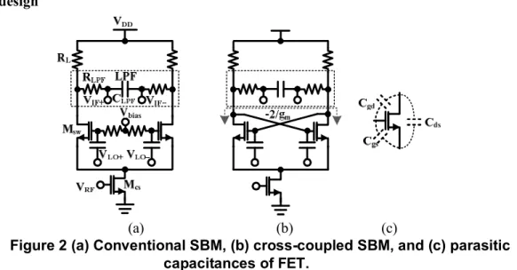
(a) (b) (c)
Figure 2 (a) Conventional SBM, (b) cross-coupled SBM, and (c) parasitic capacitances of FET.
Figure 2 shows the conventional SBM and modified cross-coupled SBM. The cross-coupled NMOS transistor pair in the VCO core is used for the coupled SBM. The impedance looking down the
cross-coupled pair provides a negative resistance of −2/gm, where gmis given by
= (1)
In Equation (1), Vgs is the gate-source voltage, Vth is the threshold voltage, and IDis the drain current.
Since the load resistance RLis in parallel with the negative resistance in Figure 2 (b), the variation of the
load resistance can partially cancel the negative resistance and control the mixer gain. When RL=−1/gm, the
maximum gain can be achieved. With the metal oxide semiconductor field effect transistor (MOSFET) transconductance of several mS, the load resistance can be chosen in the order of kΩ.
As shown in Figure 3 (a), the gain of the cross-coupled SBM continuously increase with the load resistance value until the maximum gain is achieved. In contrast, the gain of the conventional SBM saturates at some point and starts to drop with the further increase of the load resistance. For the cross-coupled SBM, the mixer gain can be controlled almost linearly in some range of the load resistance. Also, the output harmonic components at the drain nodes are severely suppressed for the cross-coupled SBM compared to that of the conventional SBM shown in Figure 3 (b) since more parasitic capacitances (Cgs, Cgd, and Cds in Figure 2 (c)) are involved at the drain nodes. The final IF spectrum is shown in Figure 3 (c) with the further suppression of the LO and its harmonics by adding the low-pass filter (LPF) at the drain nodes of the switching transistors.
For the SBM, the output current at the drain nodes of the mixer is typically given by
, = + ( − ) +. .. (2)
where ICSand gmare the dc current and transconductance of the current source MCS, respectively [7]. From (2),
the LO leakage to the output is quite strong for the SBM and this leakage can saturate the following stages of the baseband without sufficient suppression.
= (3) RL(ohm) 0 500 1000 1500 2000 2500 3000 IF V o lt a g e G a in ( d B ) 0 10 20 30 40 50 60 SBM CC SBM Freq. [GHz] 0 2 4 6 8 10 12 14 16 18 D ra in N o d e S p e c tr u m [ d B m ] -200 -150 -100 -50 0 SBM CC SBM IF=0.1 MHz fLO 3fLO 5fLO 7fLO (a) (b) Freq. [GHz] 0 2 4 6 8 10 12 14 16 18 IF S p e ct ru m [ d B m ] -200 -150 -100 -50 0 IF=0.1 MHz fLO 3fLO 5fLO 7fLO Time [sec]
0 5e-6 1e-5 2e-5 2e-5
A m p lit u d e [V ] -0.010 -0.005 0.000 0.005 0.010 IF output (CC SBM) RF input IF output (SBM) (c) (d)
Figure 3. Conventional and cross-coupled SBM performances (a) IF voltage gain, (b) drain node spectrum, (c) IF spectrum, and (c) signal swing with the RF input power of −70 dBm.
(a) (b) (c)
Figure 4. Differential VCOs (a) PLC VCO, (b) SLC VCO1, and (c) SLC VCO2. 2.2 VCO design
Figure 4 shows several types of differential VCO topologies as a candidate for LMVs. PLC VCO itself is a very simple topology with PLC network. When it is used for the LMV, the IF signal is shorted out since the
inductor is a short at the low IF frequency. To extract the IF signal, the SLC network can
Tail Current (uA)
0 500 1000 1500 2000 2500 L O O u tp u t S w in g ( V ) 0.0 0.5 1.0 1.5 2.0 2.5 SLC VCO2 RL=0.5 kOhm SLC VCO2 RL=1 kOhm PLC VCO SLC VCO1 RL=0.5 kOhm SLC VCO1 RL=1kOhm
Figure 5. Output swing of PLC and SLC VCOs.
Tail Current (uA)
0 200 400 600 800 P h a s e N o is e ( d B c /H z) -140 -120 -100 -80 -60 -40 -20 1 KHz 10 KHz 100 KHz 1 MHz PNopt
Tail Current (uA)
0 200 400 600 800 P h a se N o is e (d B c /H z) -140 -120 -100 -80 -60 -40 -20 RL=1 kOhm 1 KHz 10 KHz 100 KHz 1 MHz PNopt (a) (b)
Tail Current (uA)
0 200 400 600 800 P h a se N o is e (d B c /H z) -140 -120 -100 -80 -60 -40 -20 RL=500 Ohm 1 KHz 10 KHz 100 KHz 1 MHz PNopt (c)
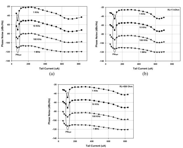
Figure 6. Phase noise performances (a) PLC VCO, (b) SLC VCO2 with RL=500 ohm, and (c) SLC VCO2 with RL=1 kohm.
be a candidate for the LMV since the inductor itself is open at the IF frequency. Figure 5 shows the VCO output swing with the tail current. For the same voltage swing, SLC VCO1 consumes a lot of current since the load resistor consumes large voltage headroom. However, SLC VCO2 in which the load resistor is directly
connected to the inductor in series consumes much less power compared to that of the SLC VCO1 and a little bit more compared to those of the conventional PLC VCO. Figure 6 shows the simulated phase noise with the tail current for the PLC VCO and SLC VCO2. As can be seen in the figure, there is an optimum phase noise point with low current consumption. For the SLC VCO2, the dc current for the optimum phase noise point
(PNopt) is a little bit larger compared to that of the PLC VCO since the load resistor consumes some voltage
headroom while the oscillation sustains. The remaining task is to trade off the phase noise, power consumption, mixer gain, and mixer noise performance.
3. LMV Design and Experimental Results
3.1 VCO as a Mixer
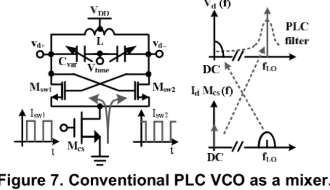
Now, the LMV can be designed combining the mixer and VCO. Figure 7 shows the conventional LC VCO in which a PLC network is used for tank circuit. The VCO performs the mixing process since an RF signal in the VCO bias current is down-converted by the switching transistors.
Figure 7. Conventional PLC VCO as a mixer.
Also, by the same mechanism, the dc current of Mcs is up-converted to the LO frequency. When this
topology is used as a down-converter, the IF signal is shorted by the inductor of the PLC tank, and severely attenuates the low-frequency component. Attempting to sense the down-converted component at the VCO output unavoidably degrades the VCO phase noise. In [3], the IF component can be extracted at the source nodes of the switching transistors as shown in Figure 1(b). Since the impedance at the IF outputs is limited by
the low impedance (2/gm) of the source nodes of the switching transistors, this topology has a low IF gain, or
requires an additional amplification at the low frequency range. This aggravates the overall noise performance of the LMV cell, and requires an additional power consumption of the low frequency amplification block [3].
The SLC VCO can be used for the LMV since the inductor the SLC network is open at the IF frequency.
3.2 LMV Design
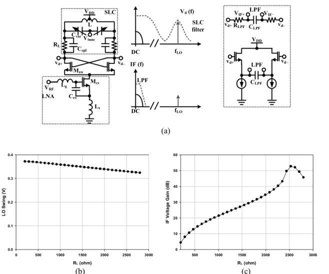
Figure 8 shows the proposed SLC LMV just by adding the SLC network to the cross-coupled SBM in
Figure 2 (b) and applying the RF signal at the gate of the current source Mcs. At the RF, the LMV is exactly
the same with the PLC VCO. At the IF, the LMV is exactly the same with the cross-coupled SBM in Figure 2 (b). Due to the strong LO leakage at the drain output, the LPF is added to suppress the LO with large capacitor,
CLPF. The LO swing does not change very much with the increasing the load resistor, RL(Too large RL will
vd VDD vd+ Msw L LPF RL C cpl Mcs VRF SLC filter fLO DC Vd(f) fLO DC IF (f) LPF SLC Vtune Cvar VIF VIF+ vd vd+RLPF CLPF Lg Ls LPF CLPF vd vd+ VDD Cex LNA (a) RL (ohm) 0 500 1000 1500 2000 2500 3000 L O S w in g ( V ) 0.0 0.1 0.2 0.3 0.4 RL (ohm) 500 1000 1500 2000 2500 3000 IF V o lt a g e G a in ( d B ) 0 10 20 30 40 50 60 (b) (c)
Figure 8. Proposed single-balanced LMV and its performances with various load resistance. (a) single-balanced LMV topology, (b) LO swing, and (c) IF voltage gain.
The IF voltage gain varies up to 40 dB linearly with the load resistor. There is a peak voltage gain at some point of the load resistor where the negative resistance cancels out the load resistor.
Figure 9. Equivalent half circuit of the SLC tank.
Figure 9 shows the half circuit of the SLC tank. The total impedance looking at the drain node of the switching pair is given by
= + || (4)
where Rpis the equivalent parallel resistance of the inductor L/2. To extract the IF signal by filtering out the
For the RC filter, the resistor RLPFneeds to be large enough not to load the tank which can make the VCO
not to oscillate. The RC LPF can be designed to attenuate the VCO output component at the drain nodes while somewhat degrading the phase noise performance.
If the capacitance value of Ccplis large enough, it can be considered as short at high frequencies and the
oscillation frequency is mainly decided by the PLC tank consisted of L and Cvar. The transistor Mcsacts as an
LNA at the RF with the inductor degeneration for 50 ohm matching, while providing the dc bias current to the VCO. At the IF, the total output resistance at the drain nodes is given by
= − || = (5)
where gmis the transconductance of the cross coupled NMOS transistor. In (5), it can be seen that the load
resistance RL can be canceled out partially with the negative resistance of the cross-coupled core and can
increase the voltage gain of the mixer.
The LNA part in Figure 8 is designed by adding a small size extra capacitor Cexbetween the gate and source
of the current source transistor, which enables to apply a power-constrained simultaneous noise input matching (PCSNIM) technique for low-power design [8, 9].
Figure 10. Small-signal equivalent circuit of the LNA.
Figure 10 shows the small-signal equivalent circuit of the LNA in Figure 8(a). The mean-squared gate induced noise current is given by
= 4 . (6) In (6), k is the Boltzmann constant, T is the absolute temperature, δ is a constant with value of 4/3 in
long-channel FET devices, Cgsis the gate-source parasitic capacitance of the RF input transistor, gd0is the
drain-source conductance at zero drain-drain-source voltage, and Δf is the bandwidth, respectively. The mean-squared channel thermal noise is given by
= 4 . (7)
The parameter has a value of unity at zero drain-source voltage and 2/3 in saturation mode operation
with long channel FET devices.
Since the gate induced noise current has a correlation with the drain channel noise current, its correlation coefficient is given by
= ∗ ≈ −0.395 (8)
The noise factor (F) and noise parameters (noise resistance Rn, optimum noise impedance Zopt, and
= 1 + ⋅ ⋅ 1 − + 1 − | | + ( ) 1 − | | + (1 − | | ) ( ) + + (9) = ⋅ (10) = ( | | ) | | ( | | ) | | − (11) = 1 +√ (1 − | | ) (12)
where γ is unity at zero VDSand 2/3 in saturation mode transistor operation with long channel devices, α=gm/gd0
is unity for long channel devices and decreases as the channel length decreases, Ct=Cgs+Cex, and ωTis the
cutoff frequency and is equal to gm/Cgs, respectively.
The input impedance Zinof the LNA is given by
= + + (13)
For the circuit shown in Figure 8, the condition for simultaneous noise and input matching can be chosen when
= = ∗ . (14)
Comparing (8) and (10), the condition that satisfy (11) is given by
( | | ) ( | | ) | | = (15) | | ( | | ) | | − = (16) = (17) − = (18)
From (15) and (17), the source degeneration inductor can be approximated by
≈ ( | | ) (19) assuming δ/γ is nearly constant which is about 2, α is less than unity, and |c|=0.395 for the short channel transistors [10].
Freq. [GHz] 0 2 4 6 8 10 12 14 16 18 IF S p ec tr u m [ d B m ] -400 -350 -300 -250 -200 -150 -100 -50 0 IF=76 kHz LO freq. Time [sec]
0 1e-5 2e-5 3e-5 4e-5 5e-5 6e-5 7e-5 8e-5
A m p lit u d e [V ] -0.0008 -0.0006 -0.0004 -0.0002 0.0000 0.0002 0.0004 0.0006 0.0008 IF output RF input (a) (b)
Figure 11. Simulated (a) IF spectrum and (b) signal swing of the proposed single-balanced LMV with RF input power of −80 dBm.
Figure 11 shows the output spectrum and signal swing of the proposed single-balanced LMV. Since the LO signal is quite large at IF, large size capacitor is connected at the IF output to reject the LO. Figure 12 shows the phase noise performance. It has the phase noise of ‒72 dBc/Hz, ‒93 dBc/Hz, and ‒113 dBc/Hz at 10 kHz, 100 kHz, and 1 MHz offset frequency, respectively. Figure 13 shows the double sideband NF of the proposed single-balanced LMV which is compared to that of the conventional SBM as shown in Figure 2 (a). The NF of the single-balanced LMV is about 7 dB lower at below the 10 kHz offset frequency and 4.3 dB lower at 1 MHz offset frequency, respectively. From the mixer theory [9], the fundamental LO and its harmonics translate the noise at the side band to the low frequency IF band. For the single-balanced LMV, the other harmonics of the LO except the fundamental LO are suppressed as shown in Figure 3 (b) and result in lower NF for the mixer. Offset Freq. [MHz] 0.001 0.01 0.1 1 P h as e N o is e [d B c/ H z] -120 -100 -80 -60 -40
Offset Freq. [MHz] 0.001 0.01 0.1 1 10 N F D S B [ d B ] 0 5 10 15 20 25 30 35 40 Conventional SBM Proposed SB LMV 4.3 dB 7 dB
Figure 13. Double sideband NF of conventional SBM and proposed single-balanced LMV.
Considering the chip implementation, a symmetric inductor is used to have a higher quality (Q) factor
(Q=12.5 at 2.4 GHz) to have a better phase noise performance. The ac coupling capacitor Ccplis implemented
with metal-insulator-metal (MIM) capacitor. The tuning range is varied with the MOS varactors. The width of
the switching transistors is 32 µm with the minimum channel length of 60 nm. The size of Lgand Lsare chosen
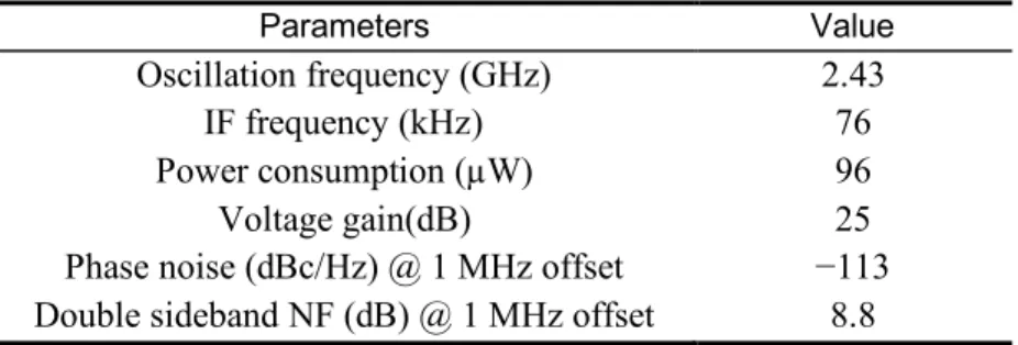
to match the signal source impedance of 50 ohm. Table I summarizes the performance of the proposed single-balanced LMV.
Table 1. Performance Summary of single-balanced LMV
Parameters Value
Oscillation frequency (GHz) 2.43
IF frequency (kHz) 76
Power consumption (µW) 96
Voltage gain(dB) 25
Phase noise (dBc/Hz) @ 1 MHz offset −113
Double sideband NF (dB) @ 1 MHz offset 8.8
4. Conclusion
This paper proposes fully integrated radio frequency front-end called LMV by merging LNA, mixer, and VCO. In the proposed single-balanced LMV, the cross-coupled differential VCO itself can be operated as a single-balanced mixer by adding parallel resistor-capacitor RC networks at the drain nodes of the differential pair while sustaining the oscillation. At the RF frequency, the RC network forms a series LC network with the tank inductor and thus the LMV itself operates as a VCO. Since the tank inductor is short and capacitor is open near dc frequency, the RC network forms the load resistors and thus the LMV itself operates as a mixer.
The proposed LMV is designed and simulated using 65 nm CMOS technology. From the simulation results, the proposed LMV is expected to be successfully integrated for the direct conversion wireless system such as smart phone, WLAN, Global Positioning System (GPS), satellite communication receiver, medical body area network, and cable TV (CATV) set-top box while consuming low power with just one integrated block.
Acknowledgement
The research was supported by a grant from the 2019 program for visiting professors overseas in Korea National University of Transportation.
References
[1] I. Kim and S. Ryu, “X-band CMOS VCO for 5 GHz Wireless LAN,” International Journal of Advanced Smart
Convergence, Vol. 9, No. 1, pp. 172-176, 2020.
[2] F. Behbahani et al., “A 27-mW GPS radio in 0.35 µm CMOS,” in Proc. IEEE Int. Solid-State Circuits Conf. Dig.
Tech. Papers. pp. 398-399, Feb. 7, 2002.
DOI: 10.1109/ISSCC.2002.993100
[3] J. van der Tang and D. Kasperkovitz, “A 0.9–2.2 GHz monolithic quadrature mixer oscillator for direct-conversion satellite receivers,” in Proc. IEEE Int. Solid-State Circuits Conf. Dig. Tech. Papers, pp. 88-89, Feb. 8, 1997. DOI: 10.1109/ISSCC.1997.585273
[4] T.-P. Wang, C.-C. Chang, R.-C. Liu et al., “A low-power oscillator mixer in 0.18-µm CMOS technology,” IEEE
Transactions on Microwave Theory and Techniques, Vol. 54, No. 1, pp. 88-95, Jan. 2006.
DOI: 10.1109/TMTT.2005.861671
[5] A. Liscidini, A. Mazzanti, R. Tonietto, L. Vandi, P. Andreani, and R. Castello, “Single-stage low-power quadrature RF receiver front-end: The LMV cell,” IEEE J. Solid-State Circuits, Vol. 41, No. 12, pp. 2832-2841, Dec. 2006. DOI: 10.1109/JSSC.2006.884824
[6] Nam-Jin Oh, “A Single-Stage Low-Power RF Receiver Front-end: Series-Resonator based LMV cell,” IETE
Technical Review, Vol. 32, No. 1, pp. 61-69, Nov. 2014.
DOI: 10.1080/02564602.2014.979376
[7] B. Razavi, RF Microelectronics, Prentice Hall, pp. 193, 1998.
[8] T.-K. Nguyen, C.-H. Kim, G.-K. Ihm et al., “CMOS low-noise amplifier design optimization techniques,” IEEE
Trans. Microw. Theory Tech., Vol. 52, No, 5, pp. 1433-1442, May. 2004.
DOI: 10.1109/TMTT.2004.827014
[9] Nam-Jin Oh, “Corrections to CMOS low-noise amplifier design optimization techniques,” IEEE Trans. Microw.
Theory Tech., Vol. 55, No. 6, pp. 1255, Jun. 2007.
DOI: 10.1109/TMTT.2007.896818
[10] T. H. Lee, The Design of CMOS Radio-Frequency Circuits, 2ndedition, Cambridge, U. K.: Cambridge Univ. Press,