Appl. Phys. Lett. 87, 013112 (2005); https://doi.org/10.1063/1.1990251 87, 013112
© 2005 American Institute of Physics.
Pressure-dependent Schottky barrier at the
metal-nanotube contact
Cite as: Appl. Phys. Lett. 87, 013112 (2005); https://doi.org/10.1063/1.1990251
Submitted: 25 January 2005 . Accepted: 25 May 2005 . Published Online: 30 June 2005 Noejung Park, Donghoon Kang, Suklyun Hong, and Seungwu Han
ARTICLES YOU MAY BE INTERESTED IN
Contact resistance between metal and carbon nanotube interconnects: Effect of work function and wettability
Applied Physics Letters 95, 264103 (2009); https://doi.org/10.1063/1.3255016 Fabrication of -type nanotube transistors with large-work-function electrodes
Applied Physics Letters 90, 092113 (2007); https://doi.org/10.1063/1.2709934 Schottky barrier formation at a carbon nanotube—metal junction
Pressure-dependent Schottky barrier at the metal-nanotube contact
Noejung Parka兲,b兲CSE Laboratory, Samsung Advanced Institute of Technology, P.O. Box 111, Suwon 440-600, Korea and Department of Applied Physics, Dankook University, Seoul 140-714, Korea
Donghoon Kang
CSE Laboratory, Samsung Advanced Institute of Technology, P.O. Box 111, Suwon 440-600, Korea Suklyun Hong
Department of Physics and Institute of Fundamental Physics, Sejong University, Seoul 143-747, Korea Seungwu Hana兲,c兲
Department of Physics and Division of Nano Science, Ewha Womans University, Seoul 120-750, Korea 共Received 25 January 2005; accepted 25 May 2005; published online 30 June 2005兲
We carry out first-principles density-functional calculations to investigate the electronic structure of the gold-carbon nanotube contact. It is found that a pressure applied on the gold-nanotube contact shifts the Fermi level from the valence edge to the conduction edge of the carbon nanotube. This can explain the n-type transport behavior frequently observed in the nanotube field-effect transistor using the gold as electrodes. An atomistic model is proposed for a possible origin of the pressure when the nanotube is embedded in the gold electrode. © 2005 American Institute of Physics. 关DOI: 10.1063/1.1990251兴
The carbon nanotube共CNT兲 is one of the promising ma-terials for the next generation of electronic devices because of its intrinsic nanoscale size, one-dimensional geometry, and excellent transport properties.1,2The high mobility, the large current density, and the controlled response to the gate voltage has been demonstrated in the nanotube-based field-effect transistor 共FET兲.3–5 Significant research efforts are now brought to the large-scale integration of CNT-FETs, es-pecially on issues such as isolation of individual nanotubes, sorting the metallic and semiconducting nanotubes, and pat-terning and integration of the electrodes and nanotubes. On the other hand, controlling the carrier type of CNT is a key issue for the development of a logic circuit, for example, nanotube-based complementary-metal-oxide semiconductor technology.
In earlier studies, it was widely accepted that the oxygen adsorption on the nanotube wall resulted in the p-type trans-port property of the FET made of as-grown nanotubes.6–8 However, the binding energy of the oxygen on the nanotube wall is rather weak and consequently the charge transfer is negligible.9–11In addition, systematic experiments indicated that the oxygen molecules affect mainly the metal electrode rather than change the carrier density of the CNT body.12,13It was shown that, irrespective of adhesion strength of the CNT to the metal electrode, the Fermi level pinning at the nano-sized contact between metal and CNT is not strong. Thus, the Schottky barrier formed at the contact is determined mostly by the difference between the metal work function and the electronic affinity of the semiconducting nanotube.14–16This raises a basic question as to why a gold electrode and CNTs without oxygen atoms frequently result in the FET having n-type transport behaviors.13 Since the gold surface has a work function 共⬃5.3 eV兲 higher than that of the CNT 共⬃4.8 eV兲, the Fermi level of the gold surface would be
closer to the valence edge and the FET device should show a p-type transport behavior. Motivated by this observation, we perform in this letter first-principles calculations on the metal-nanotube interface to investigate the Fermi level align-ment at the contact in detail. It is found that the position of Fermi level of the metal electrode within the energy gap of semiconducting CNT is a function of the metal-nanotube dis-tance and the external pressure present in the nanotube-electrode interface can cause n-type behavior of electronic transport.
The density functional calculations are carried out using the computational code of the Vienna ab initio simulation package.17 The plane-wave basis set with the energy cutoff of 400 eV is employed to describe electronic wave functions. The ionic potentials are described by the projector augmented-wave pseudopotential18 and the exchange corre-lation energy of the electrons is approximated by the gradient-corrected potential suggested in Ref. 19. The atomic positions are relaxed until the Hellmann-Feynman force on each atom is reduced to within 0.05 eV/ Å.
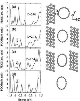
For model geometries, we choose a semiconducting 共10,0兲 nanotube placed onto or in between the Au共111兲 sur-face. The model geometries and the corresponding projected density of states共PDOS兲 for the nanotube are shown in Fig. 1.20The surfaces are modeled as three gold layers. The unit cell contains 80 carbon atoms and 54 gold atoms and the periodic boundary condition is imposed by applying strain 共corresponding to 2% compression兲 to the gold surface along the nanotube axis direction. Eight k-points are sampled in the irreducible Brillouin zone. In Fig. 1共a兲, only one side of the nanotube is in contact with the gold surface. The equilibrium distance D of 3.01 Å indicates that the adsorption is a phy-sisorption type, and the contact resistance will be significant. This corresponds to a situation where a nanotube is freely placed on the metal electrode. Since gold has a larger work function, the Fermi level is aligned at the valence band edge of the carbon nanotube, as in Fig. 1共a兲.
In many experiments, however, the electrode is depos-a兲Authors to whom correspondence should be addressed.
b兲Electronic mail: [email protected] c兲Electronic mail: [email protected]
APPLIED PHYSICS LETTERS 87, 013112共2005兲
ited lithographically after the nanotube is dispersed on the substrate. The kinetic energy of metal atoms during deposi-tion and subsequent solidificadeposi-tion will apply a finite pressure to the nanotube.21To simulate the nanotube under this com-pressive force, we artificially press the metal-nanotube-metal contact. This is conveniently mimicked by reducing the unit cell length of the supercell along the z direction关see Figs. 1共b兲 and 1共c兲兴. The most striking feature in Figs. 1共b兲 and 1共c兲 is that as the contact is pressed, the Fermi level under-goes a relative upshift and thus become aligned closer to the conduction band of the nanotube. The CNT-FET including this configuration for the contact should show a n-type trans-port behavior. The calculated quantum-mechanical stress along the z direction are 0.61 and 6.03 kbar for Figs. 1共b兲 and 1共c兲, respectively. The pressure-induced change of the transport behavior is consistent with the previous calculation reporting the increasing p-type barrier height as the metal-nanotube distance decreases.22The nonzero density of states in the band-gap region reflects the metal-induced gap states. Further increase of the compression will result in the metal-lization of the CNT.23
For comparison, the electronic density of states is plotted in Fig. 1共d兲 for the isolated 共10,0兲 nanotube with the atomic positions fixed at those in Fig. 1共c兲. We notice that the band structure is almost the same as that of the pristine nanotube. It is noticeable that the peaks corresponding to the second van Hove singularity are suppressed when the nanotube is compressed by the gold slabs, as indicated by arrows in Figs. 1共b兲–1共d兲. To understand this change in the PDOS, we ex-amine the electronic distribution of three doubly degenerate valence band states at⌫ in Fig. 2, as denoted by V1, V2, and V3. The phase change of the wave function indicated by⫾
shows that the phase of V2states changes most slowly along
the nanotube-metal contact 共dotted lines兲. Therefore, this state is easier to be hybridized with Au 6s bands compared to the V1and V3states. This explains why the second van Hove
singularity is strongly affected as the nanotube-metal dis-tance is shortened. Consequently, the Fermi level upshift along with the suppression of the van Hove singularity shown in Figs. 1共b兲 and 1共c兲 is a consequence of increased occupation of Au 6s orbitals through the hybridization with V2 states. 共See the next paragraph.兲 The pressure-induced
charge transfer from the nanotube to the gold surface will adjust the local work function of each system so that the band structure of the nanotube rigidly shifts down relative to that of the gold substrate.
In Figs. 3共a兲 and 3共b兲, the charge density differences for Figs. 1共a兲 and 1共c兲, ⌬=共CNT/Au兲−共CNT兲−共Au兲 are plotted along the z direction after being averaged over the xy plane. The origin of the z axis corresponds to the position of the topmost gold layers and the arrows indicate the outer-most carbon atoms. The electronic charge accumulates on the side of the gold surface, which indicates the larger electrone-gativity of gold and is consistent with the work function FIG. 1. The projected density of states for the共10,0兲 carbon nanotube when
it is共a兲 on the Au共111兲 surface; and 共b兲 and 共c兲 squeezed between gold slabs, respectively. The corresponding atomic structures are shown at the right of each density of state, with larger and smaller spheres representing gold and carbon atoms, respectively. The gold slab in the neighboring cell along the z direction is drawn for convenience.共d兲 The density of states for the isolated carbon nanotube compressed as in共c兲.
FIG. 2.共Color online兲 The band structure of the isolated, squeezed nanotube in Fig. 1共d兲. On the right, charge densities are shown for three doubly degenerate valence band states at⌫ point 共V1, V2, and V3兲. The ⫾ indicates the sign of the wave functions. The dotted lines indicate the metal-nanotube contact line.
FIG. 3. The electronic charge densities for Figs. 1共a兲 and 1共c兲, obtained after subtracting those of isolated gold slabs and nanotubes, are plotted along the z direction in共a兲 and 共b兲, respectively. The abscissa is measured from the topmost gold layer.
difference between CNT and gold. In Fig. 3共b兲, we note that more accumulation of the electron develops right above the gold surface共dashed circle兲 when the contact is under pres-sure. This comes from the specific Au–C hybridization, as discussed in the previous paragraph. The charge transfer in-duced by the hybridization reduces the difference of local work functions between gold and CNT, pushing the Fermi level toward the conduction edge of CNT. We also perform a similar calculation for the Au共110兲 surface to check whether the charge transfer depends on the surface orientation. The result for the 共110兲 surface is similar to that for the 共111兲 surface; that is, the Fermi level moves from the valence edge to the conduction edge as the nanotube-metal distance is re-duced.
Finally, we give a brief account on the origin of the pressure on the nanotube surface when the nanotube is em-bedded within the gold electrode. When evaporated gold par-ticles are deposited on the dielectric substrate, a planar gold surface develops with the 共111兲 orientation. Near the nano-tube, the growth of the perfect共111兲 surface is inhibited and the broken bonds or the step edges are likely to be present nearby the nanotube wall. Even though detailed and system-atic investigations on this subject is beyond the scope of the present work, a simplified model will be able to capture the essential features. In our model shown in Fig. 4, the 共5,5兲 nanotube is inserted between the two-layer gold slab. In the final relaxed structure obtained by density-functional calcu-lations, the nanotube is found to be compressed by the gold layers. The strain present in the curved gold surface is bal-anced by the compression on the nanotube wall. This is
analogous to the interface pressure when a small particle is embedded inside another material.24
One of the authors共S.H.兲 was supported by grants from the KOSEF through the Center for Nanotubes and Nano-structured Composites. Another共S.H.兲 was supported by the system IC 2010 program of the Korean government, by the National Program for 0.1 Terabit NVM Devices, and by the Sixth Strategic Supercomputing Support Program of KISTI.
1S. Iijima, Nature共London兲 354, 56 共1991兲.
2S. Frank, P. Poncharal, Z. L. Wang, and W. A. de Heer, Science 280, 1744 共1998兲.
3S. J. Tans, A. R. M. Verschueren, and C. Dekker, Nature共London兲 393, 49共1998兲.
4A. Javey, H. Kim, M. Brink, Q. Wang, A. Ural, J. Guo, P. McIntyre, P. McEuen, M. Lundstrom, and H. Dai, Nat. Mater. 1, 241共2002兲. 5A. Javey, J. Guo, Q. Wang, M. Lundstrom, and H. Dai, Nature共London兲
424, 654共2003兲.
6P. G. Collins, K. Bradley, M. Ishigami, and Z. Zettl, Science 287, 1801 共2000兲.
7G. U. Sumanasekera, C. K. W. Adu, S. Fang, and P. C. Eklund, Phys. Rev. Lett. 85, 1096共2000兲.
8S.-H. Jhi, S. G. Louie, and M. L. Cohen, Phys. Rev. Lett. 85, 1710共2000兲. 9H. Ulbricht, G. Moos, and T. Hertel, Phys. Rev. B 66, 075404共2002兲. 10P. Giannozzi, R. Car, and G. Scoles, J. Chem. Phys. 118, 1003共2003兲. 11S. Dag, O. Gülseren, T. Yildirim, and S. Ciraci, Phys. Rev. B 67, 165424
共2003兲.
12S. Heinze, J. Tersoff, R. Martel, V. Derycke, J. Appenzeller, and Ph. Avouris, Phys. Rev. Lett. 89, 106801共2002兲.
13V. Derycke, R. Martel, J. Appenzeller, and Ph. Avouris, Appl. Phys. Lett. 80, 2773共2002兲.
14F. Léonard and J. Tersoff, Phys. Rev. Lett. 84, 4693共2000兲. 15Y. Xue and M. A. Ratner, Phys. Rev. B 69, 161402共R兲 共2004兲. 16Y. Yaish, J.-Y. Park, S. Rosenblatt, V. Sazonova, M. Brink, and P. L.
McEuen, Phys. Rev. Lett. 92, 046401共2004兲.
17G. Kresse and J. Hafner, Phys. Rev. B 47, 558共1993兲; 49, 14251 共1994兲. 18P. E. Blöchl, Phys. Rev. B 50, 17953共1994兲.
19J. P. Perdew, K. Burke, and M. Ernzerhof, Phys. Rev. Lett. 77, 3865 共1996兲.
20For calculating the PDOS, the Kohn-Sham eigenstates are projected onto the Wigner-Seitz spheres centered at each atom, whose radii are chosen to be 2 and 1 Å for Au and C, respectively.
21B. Wei, P. K.-Redlich, U. Bäder, B. Heiland, R. Spolenak, E. Arzt, and M. Rühle, Ultramicroscopy 85, 93共2000兲.
22B. Shan and K. Cho, Phys. Rev. B 70, 233405共2004兲.
23S. Dag, O. Gülseren, S. Ciraci, and T. Yildirim, Appl. Phys. Lett. 83, 3180 共2003兲.
24D. A. Porter and K. E. Easterling, Phase Transformations in Metals and Alloys共Chapman & Hall, 1992兲.
FIG. 4. Model geometry for the carbon nanotube embedded in the gold slab. The strain relaxation in the regions indicated by arrows results in the pres-sure on the carbon nanotube wall.