Low-Temperature H
2S Sensors Based on Si-Coated SnO
2Nanowires
Myung Sik Choi
1, Ali Mirzaei
2,3, Jae Hoon Bang
1, Han Gil Na
1, Changhyun Jin
1,2, Wansik Oum
1,
Seungmin Han
1, Sang Sub Kim
4,*
, and Hyoun Woo Kim
1,2,*
1Division of Materials Science and Engineering, Hanyang University, Seoul 04763, Republic of Korea
2The Research Institute of Industrial Science, Hanyang University, Seoul 04763, Republic of Korea
3Department of Materials Science and Engineering, Shiraz University of Technology, Shiraz, Iran
4Department of Materials Science and Engineering, Inha University, Incheon 22212, Republic of Korea
Abstract: To attain high life standards, it is important to develop high-performance non-toxic gas sensors for public safety, environmental pollutant control, industrial processes, etc. Because reports on single element
semiconductor-coated semiconducting metal oxides for sensing applications are rare, we synthesized SnO2
nanowires and coated them with a 5 nm-thick or 10 nm-thick Si layer for H2S gas sensing studies. SnO2
nanowires were successfully synthesized using a highly pure metallic Sn powder at high temperature in a tube furnace by the vapor-liquid-solid method and Si was deposited on the nanowires by the sputtering technique. The desired morphology and composition of the synthesized nanowires were confirmed by scanning electron microscopy, transmission electron microscopy, X-ray diffraction, and energy-dispersive X-ray
spectroscopy. Moreover, the gas sensing characteristics of pristine and Si-coated SnO2 nanowires toward H2S,
CO, H2, C6H6, C2H5OH and C6H7 gases were investigated. The sensing results revealed a good response to
H2S at the optimum operational temperature of 100 °C. Notably, Si-coated SnO2 nanowire sensors showed
a better response to H2S than pristine SnO2 nanowires. The mechanism of H2S sensing is discussed in detail
here. This study shows that the Si coating on the SnO2 nanowire enhances its sensing performance and
decreases the sensing temperature required for H2S gas detection.
(Received May 3, 2019; Accepted September 7, 2019)
Keywords: SnO2, nanowires, Si, coating, H2S, gas sensor, semiconductor
1. INTRODUCTION
The considerable demand for materials with enhanced properties that can satisfy the requirements of modern
technology in the 21st century has resulted in the
development of one-dimensional nanomaterials such as nanowires [1], nanorods [2], and nanofibers [3]. Their high aspect ratios as well as good electrical, mechanical, chemical, and thermal properties [4] have led to their application in batteries [5], photocatalysts [6], fuel cells [7], gas sensors [8], etc. Gas adsorption strongly depends on the number of available adsorption sites; because nanowires provide very
high surface areas for gas adsorption, they have found particular attention in the field of gas sensors. Notably, nanowire-based gas sensors exhibit high sensitivity, short response times, and high stability; in addition, they are lightweight and can operate at lower temperatures than sensors fabricated from their bulk counterparts [9]. Therefore, several nanowire-based gas sensors have been
developed [10-13]. Stannic oxide (SnO2) is one of the most
important n-type semiconducting (Eg ~ 3.6 eV) metal oxides
[14] and has been used in gas sensors [15-17]. However, its working temperature is often high and it generally shows poor selectivity [18,19]. To address these issues, the
morphology of SnO2 nanowires has been altered [20] and n-p
junctions based on composites of SnO2 and other p-type metal
oxides [21] have been fabricated. SnO2-Si heterojunction
nanowires are promising materials for gas sensing applications. Si-based gas sensors [11] have currently received significant interest for gas sensing because of their
- Myung Sik Choi: 박사과정, Ali Mirzaei·Changhyun Jin·Sang Sub Kim·Hyoun Woo Kim: 교수, Jae Hoon Bang: 석박사통합과정, Wansik Oum·Seungmin Han:석사과정 *Corresponding Author: Sang Sub Kim
[Tel: +82-82-32-960-7546, E-mail: [email protected]] *Corresponding Author: Hyoun Woo Kim
[Tel: +82-2-2220-0382, E-mail: [email protected]] Copyright ⓒ The Korean Institute of Metals and Materials
low working temperatures [10] and compatibility with silicon technology [22]; however, their response is low [23] and their
performance needs to be improved. In the case of a SnO2-Si
sensor, SnO2 provides enhanced sensing characteristics while
Si decreases the working temperature, making the sensor highly compatible with silicon technology. Some researchers have investigated composites of Si with other metal oxides for sensing applications. For example, Zhang et al. [24]
fabricated an NO2 gas sensor based on Si/WO3 nanowires
that functioned at room temperature. Liu et al. [25] reported
NO2gas sensing with CuO/p-porous silicon heterojunctions
at room temperature. However, to the best of our knowledge, H2S sensing properties of Si-coated SnO2 nanowires have not
been investigated. In this work, Si-coated SnO2 nanowires
were synthesized by thermal evaporation, and then, Si was
sputtered on the nanowires. The fabricated Si-coated SnO2
nanowires demonstrated an enhanced response to H2S
compared to pristine SnO2 nanowires. The sensing mechanisms
are explained in detail in this report.
2. EXPERIMENTAL PROCEDURE
2.1 Synthesis
SnO2 nanowires were produced in a tube furnace. For the
synthesis, metallic Sn nanopowder with a purity of 99.9% was used as the raw material. Typically, a 3 nm-thick Au layer was coated on a Si substrate as catalyst; the Au-coated substrate was heated at 900 °C for 1 h, and then, exposed to
a mixture of Ar (97%) and O2 (3%) gases at a constant flow
rate and total pressure of 2 Torr. The details of the SnO2
nanowire synthesis have been reported in our previous publications [26,27].
Si was coated on the as-grown SnO2 nanowires by radio
frequency (RF) sputtering with a Si target at room temperature. The optimal pressure for the Si shell layer deposition was 10 mTorr in Ar ambient and the RF power during the deposition was set to 50 W. The sputtering time was varied from 2 min to 4 min to obtain Si shells with thicknesses of 5 nm and 10 nm, respectively.
2.2 Material Characterization
The crystallinity and phase purity of the prepared samples were investigated by X-ray diffraction (XRD) using a Philips
X’Pert diffractometer with the Cu Kα1 radiation (λ = 1.5404
Å). The morphology was investigated by scanning electron microscopy (SEM, Hitachi S-4200) and transmission electron microscopy (TEM, Philips CM 200). Energy-dispersive X-ray spectroscopy (EDS) was performed to study the chemical composition of the synthesized products. The work function
of SnO2 nanowires was determined from the ultraviolet
photoelectron spectroscopy (UPS) profiles recorded using an HeI (21.2 eV) ultraviolet source.
2.3 Sensor Fabrication and Gas Sensing Tests Details of the gas sensing tests can be found elsewhere [28-30]. A bi-layered electrode comprising a Au layer (300 nm-thick) and a Ti layer (50 nm-nm-thick) was sputter-deposited on each sample. The gas flow was controlled by changing the mixing ratio of dry air to the target gas using mass flow controllers under a total stream of 500 sccm. All measurements were carried out in a special gas chamber and the sensor resistance data were obtained using a source meter. The sensor response (R) is defined as R = Ra/Rg, where Ra
and Rg are the resistances of the sensor in air and in the
presence of the target gas, respectively. The response and recovery times were calculated as the time to reach 90% of the final signal after exposure and stoppage of the target gas, respectively.
3. RESULTS AND DISCUSSION
3.1 Morphological and Structural Studies
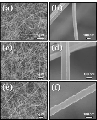
The morphology of the synthesized nanowires was studied by SEM and the micrographs are presented in Fig. 1 (a)-(f). Fig. 1(a) reveals bare, curvy, and continuous SnO2 nanowires
with lengths in the order of several micrometers and diameters of ~100 nm. Figure 1(b) is a high-magnification SEM image showing the smooth morphology of the
synthesized bare SnO2 nanowires. Figure 1(c) shows
Si-coated SnO2 nanowires with a shell thickness of 5 nm and the
high-magnification SEM image in Fig. 1(d) shows the relatively smooth morphology of the coated nanowires. Figure 1(e) and (f) show the SEM images of Si-coated (10
nm) SnO2 nanowires. Coating with a 10 nm Si shell resulted
in a relatively rough morphology.
nanowires, XRD patterns of bare and Si-coated SnO2
nanowires were recorded and are shown in Fig. 2(a)-(c).
Common peaks for all materials were observed at 2θ = 26.61, 33.92, 37.99, 39.02, 51.83, 54.81, and 57.91°, corresponding to the (110), (101), (200), (111), (211), (220), and (002)
planes of SnO2, respectively. Si peaks at 2θ = 26.87 (200),
33.07 (211), 38.37 (220), 51.53 (321), 55.38 (400), and 59.06° (411), originating from the Si shell, overlapped with the SnO2 peaks. In addition, the microstructures of bare and
Si-coated SnO2 nanowires were studied by TEM and the
micrographs are presented in Fig. 3. TEM images of SnO2
nanowires with shell thicknesses of 5 nm and 10 nm are shown in Fig. 3(a) and 3(d), respectively. As observed, the
Fig. 1. SEM images of (a) and (b) bare SnO2 nanowires, (c) and (d)
SnO2 nanowires with 5 nm-thick Si shells, and (e) and (f) SnO2 nanowires with 10 nm-thick Si shells.
Fig. 2. XRD patterns of (a) bare SnO2 nanowires and SnO2
nanowires with Si shell thicknesses of (b) 5 nm and (c) 10 nm.
Fig. 3. (a) TEM and (b) HRTEM images and (c) SAED pattern of SnO2 nanowires with a shell thickness of 5 nm. (d) TEM and (e) HRTEM
nanowires were long and separate from one other, suggesting that they can provide high surface areas for gas adsorption. The diameters of the nanowires were about 100 nm, in accordance with the SEM results. The high-resolution TEM
(HRTEM) images of SnO2 nanowires with shell thicknesses
of 5 nm and 10 nm are shown in Fig. 3(b) and 3(e), respectively. In both cases, lattice fringes with spacings of 0.264 nm and 0.237 nm, corresponding to the (101) and (200)
planes of SnO2, respectively, were observed. This result
further confirmed the crystalline nature of the SnO2
nanowires. The corresponding selected area diffraction (SAED) patterns showing distinct diffraction spots are presented in Fig. 3(c) and 3(f) which confirms the single
crystalline nature of the synthesized SnO2 nanowires. The
EDS elemental mapping images revealing the presence Si, Sn, and O in the synthesized nanowires are shown in Fig. 4. It is
noteworthy that a thin Si layer covered the SnO2 nanowires.
3.2 Gas Sensing Studies
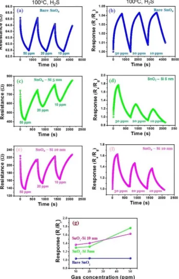
From a series of preliminary tests, we determined that the optimal working temperature of the sensors was 100 °C; therefore, all gas sensing measurements were performed at
100 °C. Fig. 5 shows the H2S sensing properties of bare and
Si-coated SnO2 nanowires. The dynamic response plots of
bare SnO2 nanowires for 10, 20, and 50 ppm of H2S gas are
shown in Fig. 5(a). Upon exposure to H2S gas, the resistance
of the sensor decreased, reflecting its n-type behavior. Furthermore, the response was reversible, because after stopping the injection of H2S and air, the resistance returned
to its initial value. The response (Ra/Rg) versus time plots are
presented in Fig. 5(b). The responses of the bare SnO2
nanowire sensor to 10, 20, and 50 ppm H2S gas were 1.035,
1.043, and 1.043, respectively, indicating that the response was almost identical for different concentrations of H2S gas.
This was likely due to the limited surface area of the bare
SnO2 nanowire. The dynamic response plots of 5 nm-thick
and 10 nm-thick Si shell-coated SnO2 nanowires for different
concentrations of H2S are shown in Fig. 5(c) and 5(e),
Fig. 4. EDS elemental mapping images showing the presence of Si, Sn, and O.
Fig. 5. Dynamic responses of (a) bare SnO2 nanowires and SnO2
nanowires with Si shell thicknesses of (c) 5 nm and (e) 10 nm toward 10, 20, and 50 ppm of H2S gas at 100 °C. Response of (b)
bare SnO2 nanowires and SnO2 nanowires with shell thicknesses of (d) 5 nm and (f) SnO2 10 nm toward 10, 20, and 50 ppm of H2S gas
respectively. Both sensors showed n-type behaviors and reversible responses. Fig. 5(d) and 5(f) show plots of
response as a function of time for SnO2 nanowires coated
with 5 nm- or 10 nm-thick Si shells. The responses of SnO2
nanowires with 5 nm Si shells to 10, 20, and 50 ppm of H2S
gas were 1.299, 1.321, and 1.769, respectively, while those of
SnO2 nanowires with 10 nm-thick Si shells were 1.367,
1.405, and 1.629, respectively. The calibration curves of all sensors are shown in Fig. 5(g). Clearly, the response of bare
SnO2 nanowires was far lower than that of Si-coated SnO2
nanowires. This demonstrated that Si enhanced the sensing
performance of the SnO2 nanowire. Furthermore, the
nanowires with 5 nm-thick Si shells showed a higher
response to 50 ppm of H2S than those with 10 nm-thick
shells; on the other hand, to 10 ppm and 20 ppm of H2S, the
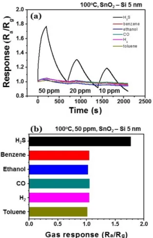
response of nanowires with 5 nm-thick Si shells was higher. Selectivity for a target gas is highly important for real
applications because a lack of selectivity can lead to false alarms, limiting the practical application of a sensor. To study the selectivity of 5 nm-thick Si shell-coated SnO2 nanowires,
they were exposed to 50 ppm of benzene, ethanol, CO, H2,
and toluene gases at 100 °C. Fig. 6(a) shows the variations in responses to these gases with time; the corresponding selectivity histogram of the sensor is presented in Fig. 6(b). The sensor responses to the gases were 1.051, 1.028, 1.052, 1.047, and 1.016, respectively, indicating that these sensors were largely insensitive to interfering gases.
3.3 Gas Sensing Mechanism
Several factors can influence the sensing behavior of
Si-shelled SnO2 nanowires. When considering the changes in
the resistance of a SnO2-Si core-shell nanowire upon
exposure to H2S gas, the change in the resistance of the SnO2
nanowire core (R1) and the change in the resistance of the Si
shell (R2) should be taken into account [28]. Almost every
gas adsorbs onto the surface of a metal oxide [31]. The most prominent reactive gas in normal ambient air is molecular oxygen. Depending on the sensor operation temperature, oxygen adsorbs in various forms onto the metal oxide
surface. Exposure of a pristine SnO2 nanowire sensor to air
results in the adsorption of oxygen molecules onto the surface of the nanowire. Because of the high electron affinity of oxygen, the adsorbed oxygen molecules trap electrons
from the conduction band of SnO2, forming ionized oxygen
species such as , , and [2]:
(3) (4) (5) (6) Consequently, the concentration of electrons on the surface
decreases, and accordingly, the resistance of the SnO2
nanowires increases. When a pristine SnO2 nanowire gas
sensor is exposed to H2S, H2S molecules chemisorb on the
surface of the SnO2 nanowire, and electrons are released by
a subsequent reaction with oxygen ions, resulting in H2O and
SO2 gases [32]: (7) O2– O– O2 – O2 gas( )→O2 ads( ) O2 ads( )+e=O2 ads–( ) O2 ads–( )+e=2O(–ads) O(–ads)+e=O(2 ads– ) H2S(ads)=3O–(ads)=SO2 g( )+H2O 3e+
Fig. 6. (a) Transient response of SnO2-Si (10 nm) sensor toward
different gases at 100 °C. (b) Selectivity histogram of SnO2-Si (5 nm) sensor to 50 ppm of gases tested at 100 °C.
The released electrons decrease the resistance of the gas
sensor, resulting in a response. Because the core SnO2
nanowires were single crystalline, the effects of grain
boundaries were excluded. After Si was coated on the SnO2
nanowires, an increase in response was observed. As observed in Fig. 5(g), the response of the Si-shelled nanowires was superior to that of bare nanowires, regardless of the gas
concentration or shell thickness. The H2S gas sensing
mechanism for the Si-coated SnO2 nanowire sensor can be
explained on the basis of several factors. The TEM results revealed that the Si shell layer did not completely cover the core nanowire, wherein a part of the core was exposed along the entire length of the nanowire. More importantly, the sensor exhibited an n-type behavior, illustrating the dominant role of
the SnO2 nanowire core in sensing.
Similar to that for the SnO2 nanowires, adsorption of H2S
gas likely changed the resistance of the Si shell layer. When
SnO2 nanowires with Si shell layers were exposed to H2S,
electrons were released, as shown in Eq. (7). Because the Si shell layer had a p-type semiconducting property, the adsorption of H2S gas resulted in the donation of electrons or
extraction of holes, generating a hole depletion region. Thus,
when H2S gas was introduced, the resistance of the Si shell
layer increased. Furthermore, because the Si shell layer was polycrystalline, modulation of resistance might occur along grain boundaries.
An important difference between the pristine and Si-coated
SnO2 nanowire sensors is the existence of Si-SnO2 p-n
junctions. Notably, SnO2/Si heterointerfaces affect the sensing
behavior. In particular, the conductivity, accumulation of electrons, and size of the electron depletion region prior to H2S
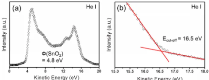
introduction will determine the sensor response. The work function of SnO2 is reported to be in the range of 4.0-5.7 eV
[33-47]. In this study, the work function of SnO2 nanowires
was measured to be 4.8 eV. From the UPS profile of SnO2, the
cut-off value was determined to be 16.5 eV (Fig. 7). The work function was calculated by subtracting the cut-off value from the reference value of 21.1 eV. To correct the broadening due to the analyzer, 0.1 eV was added to each work function value.
Accordingly, the work function of the SnO2 nanowire was
calculated to be 4.8 eV (= 21.2 eV – 16.5 eV + 0.1 eV). Previous studies have reported that the work function of Si falls within the range of 4.1-5.0 eV [48-60]. In particular, the
work function of p-type Si is 4.7-5.0 eV [59]. There are two possible explanations for the enhanced response observed in the presence of the Si shell, both of which depend on the relative magnitudes of the work functions.
One possibility is that the Fermi level (EF) of p-Si is higher
than that of SnO2. In this case, the work function of SnO2 will
be larger than that of p-Si. Therefore, electrons from p-Si will
flow to SnO2 to balance the Fermi levels. At the same time,
holes from SnO2 will flow to p-Si. Consequently, electron and
hole accumulation layers will be generated on the SnO2 and
p-Si sides of the heterojunction, respectively. Subsequently, the
conduction volume of the SnO2 core will increase and a
corresponding change in the conduction volume due to the introduction/removal of H2S gas will generate a lower sensor
response. The other possibility is that the Fermi level (EF) of
p-Si is lower than that of SnO2 (Fig. 8(a)). In this case, the
work function of SnO2 will be smaller than that of p-Si. Thus,
electrons from SnO2 will flow to p-Si (Fig. 8(b)).
Consequently, electron and hole depletion layers will be
generated on the SnO2 and p-Si sides of the heterojunction,
respectively. Subsequently, the initial conduction volume in the SnO2 core will decrease and a corresponding change in the
conduction volume due to the introduction/removal of H2S
gas will generate a higher sensor response. As observed in Fig. 5(g), the addition of the Si shell layer enhanced the response of the bare nanowire sensor, indicating that the work function of SnO2 was smaller than that of p-Si in this work.
Moreover, the deposition of Si onto the SnO2 nanowires might
introduce structural defects, favoring the adsorption of the target gas as well as oxygen molecules, and thereby, leading to an increase in the sensor signal [29].
A schematic diagram of the sensing mechanism for the fabricated sensors is given in Fig. 9. Notably, the TEM results showed that the shell layer was partially open, in other
Fig. 7. (a) UPS profile of SnO2 nanowires. (b) Calculation of cut-off
words, the shell layer partially covered the core SnO2
nanowire. Because the shell was preferentially deposited on one side of the core nanowire, the shell was partially open
and a considerable part of the SnO2 core was exposed to air
ambient. Accordingly, electron currents in the n-SnO2 core
and hole currents in p-Si contributed to the sensing behavior. Because of the work function difference between Si and SnO2 in air and exposure of the bare surfaces to air, a hole
accumulation layer, a hole depletion layer, and an electron depletion layer were formed (see Fig. 9(a)). As shown in Fig. 9(a), the hole and electron depletion layers were formed on
the p-Si and n-SnO2 sides, respectively, at the interface
between p-Si and n-SnO2. Upon exposure to H2S, electrons
returned to the surface of the sensing layer, decreasing the width of the electron and hole depletion layers and the hole accumulation layer, as shown in Fig. 9(b).
The introduction of H2S gas resulted in a decrease in the
resistance of both bare and Si-coated SnO2 nanowire sensors.
Thus, the sensors exhibited n-type behaviors. Accordingly, we surmised that the main sensing current was the electron
current flowing through the n-type SnO2 nanowire core,
although both electron and hole currents flowed; notably, a change in the transport mode enhanced the sensing behavior. To the total resistance induced by introduction of H2S, the
contribution by the SnO2 core was higher than that by the Si
shell. Because sensor total current comprises an SnO2 core
and a Si-shell in parallel, the equivalent resistance Req could
be defined by the following equation: 1/Req = 1/Rn + 1/Rp,
where Rn and Rp are the resistances of the n-type core and
p-type shell, respectively. Because the total resistance
(equivalent resistance) was smaller than Rn and Rp, the
simultaneous presence of the SnO2 core and Si-shell
generated a higher sensor response.
As shown in Fig. 6, the fabricated sensor exhibited selectivity toward H2S gas. The Si shell layer contributed to
enhancement of the sensing activity of the sensor. The Si
shell was covered with a thin native oxide (SiOx) layer due
to the exposure of the Si shell to air. This resulted in a
Fig. 8. (a) Band structure of n-SnO2 and p-Si before contact and (b)
after contact in air. Fig. 9. Schematic illustration of variation in the conduction channel of SnO2 nanowire coated with Si in (a) air and (b) H2S atmospheres.
(HAL: hole accumulation layer, HDL: hole depletion layer, EDL: electron depletion layer)
significant decrease in the sensing activity, because of insulating characteristics of silicon oxide. Thus, possibly H2S
gas molecules attacked and partially removed the SiOx layer.
Another possibility is that H2S decomposed, generating H2
gas species by the following reaction: 2H2S → 2H2 + S2. This
reaction has been reported to easily occur at high temperatures in the presence of metal catalysts, sulfide catalysts, and sulfur bacteria [30]. Although the sensing
temperature in the present work was not high, possibly SnO2
or interstitial Sn played a catalytic role in the decomposition
of H2S. The generated H2 might have reacted with SiOx,
leading to the removal of the silicon oxide layer. The other possibility is that H2S gas molecules directly reacted with the
silicon oxide layer according to the following reaction: SiO2
+ 2H2S → SiS2 + 2H2O. However, the Gibbs free energy for
the above reaction is positive at the sensing temperature of 100 °C; therefore, the direct reaction of H2S with the native
oxide would not have contributed to the removal of the oxide layer [61,62].
4. CONCLUSIONS
In conclusion, uncoated and Si-coated (5 nm and 10 nm)
SnO2 nanowires were synthesized and their gas sensing
performances were investigated. At the optimal operation
temperature (100 °C), the response of Si-coated SnO2
nanowires to H2S was higher than that of bare SnO2
nanowires. The responses of SnO2 nanowires with 5
nm-thick Si shells and 10 nm-nm-thick Si shells were highly similar.
However, at a high H2S concentration (50 ppm), the response
of SnO2 nanowires with 5 nm-thick Si shells was higher than
that of SnO2 nanowires with 10 nm-thick Si shells (1.769
versus 1.629). The removal of the native SiOx layer by H2S
gas, creation of p-n heterojunctions, modulation of the
conduction channels of both SnO2 and Si, and creation of
imperfections in Si-coated SnO2 nanowires were the main
reasons for the improved response to H2S gas. Si-coated
SnO2 nanowire sensors were tested in other gas atmospheres,
and the sensors revealed good selectivity to H2S gas
compared to CO, benzene, toluene, and H2. The present study
shows that coating metal oxides with Si can enhance their sensing response and decrease the optimal sensing temperature.
ACKNOWLEDGMENTS
This research was supported by the Basic Science Research Program through the National Research Foundation of Korea (NRF) funded by the Ministry of Education (2016R1A6A1A03013422). This work was also supported by the NRF grant funded by the Korean government (MSIT; 2019R1A2C1006193) and this work was also supported by the research fund of Hanyang University (HY-2019).
REFERENCES
1. R. Lee, M. H. Jo, T. W. Kim, H. J. Kim, and J. C. Shin, Electron. Mater. Lett. 14, 357 (2018).
2. A. Mirzaei, S. Park, H. Kheel, G.-J. Sun, S. Lee, and C. Lee, Ceram. Int. 42, 6187 (2016).
3. J. H. Lee, Y. S. Park, M. J. Jang, S. M. Park, K. H. Lee, W. S. Choi, S. M. Choi, and Y. D. Kim, Korean, J. Met. Mater. 56, 885 (2018).
4. S. V. N. T. Kuchibhatla, A. S. Karakoti, D. Bera, and S. Seal, Prog. Mater. Sci. 52, 699 (2007).
5. J. Chen, L. N. Xu, and W. Y. Li, Adv. Mater. 17, 582 (2005). 6. M. Xu and J. Zhao, Electron. Mater. Lett. 14, 499 (2018). 7. Z. Wen, S. Ci, S. Mao, S. Cui, G. Lu, K. Yu, S. Luo, Z. He,
and J. Chen, J. Power Sources 234, 100 (2013).
8. S.-J. Choi and I.-D. Kim, Electron. Mater. Lett. 14, 221
(2018).
9. X. Chen, C. K. Y. Wong, C. A. Yuan, and G. Zhang, Sens.
Actuators B-Chem. 177, 178 (2013).
10. J. Liao, Z. Li, G. Wang, C. Chen, S. Lv, and M. Li, Phy.
Chem. Chem. Phys. 18, 4835 (2016).
11. C. R. Field, H. J. In, N. J. Begue, and P. E. Pehrsson, Anal. Chem. 83, 4724 (2011).
12. S. Kim, J. H. Bang, M. S. Choi, W. Oum, A. Mirzaei, N. Lee, H.-C. Kwon, D. Lee, H. Jeon, S. S. Kim, and H. W. Kim, Met. Mater. Int. 25, 805 (2019).
13. H. S. Woo, C. H. Kwak, I. D. Kim, and J. H. Lee, J. Mater.
Chem. A 2, 6412 (2014).
14. L. L. Wang, L. P. Kang, H. Y. Wang, Z. P. Chen, and X. J. Li, Sens. Actuators B-Chem. 229, 513 (2016).
15. G.-J.Sun, J. K. Lee, W. I. Lee, R. P. Dwivedi, C. Lee, and T. Ko, Electron. Mater. Lett. 13, 260 (2017).
16. H. W. Kim, H. G. Na, Y. J. Kwon, H. Y. Cho, and C. Lee,
Sens. Actuators B-Chem. 219, 22 (2015).
17. V. Srivastava and K. Jain, Mater. Lett. 169, 28 (2016).
15119 (2016).
19. G. Neri, A. Bonavita, G. Micali, N. Donato, F. A. Deorsola, P. Mossino, I. Amato, and B. De Benedetti, Sens. Actuators
B-Chem. 117, 196 (2006).
20. S. S. Kim, H. G. Na, H. W. Kim, V. Kulish, and P. Wu, Sci. Rep. 5, 1 (2015).
21. S.-W. Choi, A. Katoch, G.-J. Sun, J.-H. Kim, S.-H. Kim, and S. S. Kim, ACS Appl. Mater. Interfaces 6, 8281 (2014). 22. S. Ozdemir and J. L. Gole, Curr. Opin. Solid State Mater.
Sci. 11, 92 (2007).
23. Y. F. Zhang, Y. H. Tang, N. Wang, D. P. Yu, C. S. Lee, I. Bello, and S. T. Lee, Appl. Phys. Lett. 72, 1835 (1998). 24. W. Zhang, M. Hu, X. Liu, Y. Wei, N. Li, and Y. Qin, J.
Alloy. Compd. 679, 391 (2016).
25. X. Liu, M. Hu, Y. Wang, J. Liu, and Y. Qin, J. Alloy. Compd. 685, 364 (2016).
26. H. W. Kim and S. H. Shim, J. Korean Phys. Soc. 47, 516
(2005).
27. H. W. Kim, J. W. Lee, S. H. Shim, and C. Lee, J. Korean Phys. Soc. 51, 198 (2007).
28. D. T. T. Le, D. D. Trung, N. D. Chinh, B. T. Thanh, H. S. Hong, N. Van Duy, N. D. Hoa, and N. Van Hieu, Curr. Appl. Phys. 13, 1637 (2013).
29. S. Park, S. Kim, G.-J. Sun, S. Choi, S. Lee, and C. Lee, Ceram. Int. 41, 9823 (2015).
30. S. An, J. Thermodyn. Catal. 8, 1000186 (2017).
31. S. Park, S. Park, J. Jung, T. Hong, S. Lee, H. W. Kim, and C. Lee, Ceram. Int. 40, 11051 (2014).
32. P. S. Shewale, Y. S. Yu, J.-H. Kim, C. R. Bobaded, and M. D. Uplane, J. Anal. Appl. Pyrolysis 112, 348 (2015). 33. D. L. Feucht, J. Vac. Sci. Technol. 14, 57 (1977).
34. M. N. Islam and M. O. Hakim, J. Mater. Sci. Lett. 5, 63
(1986).
35. R. G. Gordon, MRS Bull. 25, 52 (2000).
36. S. Gubbala, H. B. Russell, H. Shah, B. Deb, J. Jasinski, H.
Rypkema, and M. K. Sunkara, Energy Environ. Sci. 2, 1302
(2009).
37. J.-H. Kim, H. W. Kim, and S. S. Kim, Sens. Actuators B-Chem. 239, 578 (2017).
38. S.-W. Choi, A. Katoch, J. Zhang, and S. S. Kim, Sens.
Actuators B-Chem. 176, 585 (2013).
39. S.-W. Choi, A. Katoch, G.-J. Sun, and S. S. Kim, Sens.
Actuators B-Chem. 181, 787 (2013).
40. J. Y. Park, S.-W. Choi, and S. S. Kim, J. Phys. D. Appl. Phys. 44, 205403 (2011).
41. A. Katoch, Z. U. Abideen, H. W. Kim, and S. S. Kim, ACS
Appl. Mater. Interfaces 8, 2486 (2016).
42. J.-H. Kim, P. Wu, H. W. Kim, and S. S. Kim, ACS Appl. Mater. Interfaces 8, 7173 (2016).
43. S.-W. Choi, A. Katoch, J.-H. Kim, and S. S. Kim, ACS Appl. Mater. Interfaces 6, 17723 (2014).
44. Y. J. Kwon, H. G. Na, S. Y. Kang, M. S. Choi, J. H. Bang, T. W. Kim, A. Mirzaei, and H. W. Kim, Sens. Actuators B-Chem. 239, 180 (2017).
45. J.-H. Kim, J.-H. Lee, A. Mirzaei, H. W. Kim, and S. S. Kim,
Sens. Actuators B-Chem. 248, 500 (2017).
46. M. Batzill and U. Diebold, Prog. Surf. Sci. 79, 47 (2005). 47. X. Fang, J. Yan, L. Hu, H. Liu, and P. S. Lee, Adv. Funct.
Mater. 22, 1613 (2012).
48. R. S. Becker, G. S. Higashi, Y. J. Chabal, and A. J. Becker, Phys. Rev. Lett. 65, 1917 (1990).
49. L. Hao, Y. Liu, W. Gao, Y. Liu, Z. Han, L. Yu, Q. Xue, and J. Zhu, J. Alloy. Compd. 682, 29 (2016).
50. X. Li, H. Zhu, K. Wang, A. Cao, J. Wei, C. Li, Y. Jia, Z. Li, X. Li, and D. Wu, Adv. Mater. 22, 2743 (2010).
51. R. M. Feenstra, J. A. Stroscio, and A. P. Fein, Surf. Sci. 181, 295 (1987).
52. P. Dwivedi, N. Chauhan, P. Vivekanandan, S. Das, D. S.
Kumar, and S. Dhanekar, Sens. Actuators B-Chem. 249,
602 (2017).
53. D. Yan, S. Li, S. Liu, M. Tan, and M. Cao, J. Alloy. Compd. 735, 718 (2017).
54. W. Yan, M. Hu, D. Wang, and C. Li, Appl. Surf. Sci. 346,
216 (2015).
55. W. Yan, M. Hu, J. Liang, D. Wang, Y. Wei, W. Zhang, and Y. Qin, Mater. Res. Bull. 83, 453 (2016).
56. Y. Qin, Z. Cui, T. Zhang, and D. Liu, Sens. Actuators B-Chem. 258, 246 (2018).
57. A. Kobayashi, F. Grey, R. S. Williams, and M. Aono, Science 259, 1724 (1993).
58. L.-W. Wang and A. Zunger, J. Chem. Phys. 100, 2394
(1994).
59. H. Tai, X. Xu, Z. Ye, C. Liu, G. Xie, and Y. Jiang, Chem. Phys. Lett. 621, 58 (2015).
60. Y. Liu, L. Hao, W. Gao, Z. Wu, Y. Lin, G. Li, W. Guo, L. Yu, H. Zeng, J. Zhu, and W. Zhang, Sens. Actuators B-Chem. 211, 537 (2015).
61. I. Barin, Thermochemical Data of Pure Substances, 3rd ed., Wiley, New Jersey (1997).
62. R. Lee, M. H. Jo, T. W. Kim, H. J. Kim, and J. C. Shin, Electron. Mater. Lett. 14, 357 (2018).