Electronically Tunable Current gain FTFN using OTAs
Somjai Arayawat, Amphawan Chaikla, Vanchai Riewruja, and Thanit Trisuwannawat
Faculty of Engineering, King Mongkut’s Institute of Technology Ladkrabang, Bangkok, Thailand(Tel : +66-2-739-0758; E-mail: [email protected])
Abstract: This paper presents the realization of a four-terminal floating nullor (FTFN), which is simple configuration comprised three OTAs. The external bias currents of the OTAs can electronically adjust the current gain of the proposed FTFN. The realization method is suitable for implementation in monolithic integrated form. To demonstrate the circuit performances, the proposed FTFN was simulated by the use of the PSPICE analog simulation program and implemented using the commercially available OTAs. The simulation and experimental results verifying the performances of the proposed circuit are agreed with the theoretical values. Some application example in the design of the proposed FTFN as electronically tunable active element are also included.
Keywords: FTFN, OTAs-based circuit, tunable current gain nullor
1. INTRODUCTION
Tellegen has introduced a concept of ideal amplifier with zero input current and voltage since 1954 [1]. It sets the guidelines for presentation of the nullor by Calin in 1964 [2]. The four-terminal floating nullor (FTFN) consists of two pathological two-terminal elements called a nullator and norator. The nullator found at FTFN input port, whose current and voltage are always constrained to zero. The norator found at FTFN output port, whose current and voltage have undefined values. ‘Floating’ [3] is used here to define that no current is internally leaking always from the port and the current and voltage of the port is not internally dependent on the common-mode voltage of that port.
The concept of FTFN has proven to be the universal active element to syntheses the filters [4], inverse filter [5] and sinusoidal oscillator [6]. Accordingly, there has been much effort to present the implementations of FTFN in integrated circuit technique [7-9]. These approaches have not been implemented with variable current gain. When the current gain of FTFN can be electronically adjusted, the advantage will be gained [10]. This approach is based on the use of operational amplifier (op-amp) and two current mirrors as circuit building blocks. This paper aims to present the similar FTFN with electronically tunable current gain. We develop this idea in the difference way to realize FTFN using three operational transconductance amplifiers (OTAs). This is due to the fact that OTAs are low-cost devices and their transconductance gain can be linearly controlled over more than four decades by means of an external bias current. The allpass filter was implemented using the proposed FTFN as an illustrative application example to demonstrate the advantage of the proposed circuit.
2. CIRCUIT DESCRIPTION
Y X Z W IY = 0 VY VX IW IX = 0 IZ = kIWFig. 1 Model of tunable current gain FTFN Fig. 1 shows the model of the tunable current gain FTFN (abbreviated as TFTFN). The port relations can be characterized by
Y X 0
I =I = , VY=VX, IZ=kIW (1) where k is the current gain of TFTFN.
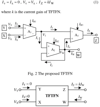
A1 VY IY Y + -A2 VX X + -A3 -+ IB1 IB2 IB3 IX IZ Z V1 -IW VW W I3 I1 I2 I4
Fig. 2 The proposed TFTFN
TFTFN Y X Z W VY VX IY = 0 IX=0 IZ = kIW IW
Fig. 3 Circuit symbol of the proposed TFTFN The proposed circuit as shown in Fig. 2 comprises of three OTAs. It is desirable that all OTAs with closely matched characteristics are used. Fig. 3 shows the circuit symbol of the proposed TFTFN. Since the OTAs A1-A3 operate as the transconductance amplifier with very high input impedance [11]. Therefore, their input currents are equal to zero written as Y X 0 I =I = (2) 0 2 1= I = I (3) 0 4 3= I = I (4) The output current of each OTA as a function of the differential voltage between its inputs can be given by
(
Y X)
1 3 g V V I = m − (5)(
W 1)
2V V g IW = m − (6) ICCAS2005 JUNE 2-5, KINTEX, Gyeonggi-Do, Korea(
W 1)
3V V
g
IZ = m − (7) The transconductance gain gmi of the OTA Ai is equal to IBi/2VT. Where IBi and VT are the external bias current of the of OTA Ai and the thermal voltage, respectively. Substituting Eq. (4) into Eq. (5), the input voltages of Y-terminal and X-terminal can be stated as
X
Y V
V = (8) Based on Eqs. (6)~(7), if we design gm3 = kgm2. The relation
between the output current IW and IZ can be rewritten as
W B2 B3 W Z I I I kI I = = (9)
where k = gm3/gm2 = IB3/IB2. Eq. (9) shows that the external bias current IB2 and IB3 of the OTA A2 and A3 can electronically adjust the current gain of the proposed TFTFN.
Based on Eqs. (2), (8), and (9), it is clearly seen that the proposed circuit in Fig. 2 similarly functions as the tunable current gain FTFN as referred in Eq. (1).
3. RESULTS AND APPLICATION EXAMPLE
3.1 Simulation results and application example
The performances of the proposed circuit were studied by the use of PSPICE analog simulation program. The simulation results was carried out using commercial OTA model as LM13600N. The power supply voltage are set to ±10V. The bias current of the OTAs IB1 and IB2 are set to 0.5mA. TFTFN Y X Z W VY IY = 0 IZ = kIW IW + RW RZ
-Fig. 4 TFTFN-based voltage-to-current converter
IB3 (mA) 0 0.2 0.4 0.6 0.8 1.0 250 500 IZ (uA) Ideal Measured
Fig. 5 Simulated results of the current gain k against the ratio of bias currents IB3 and IB2
1.0 100 10K 1.0M 100M -20 -10 0 10 Frequency (Hz) IB3 = 0.25mA IB3 = 0.5mA IB3 = 1mA C urre nt ga in, k = IB3 /IB2 (dB )
Fig. 6 Simulated results of the current gain k against the frequency
To verify the current transfer characteristic of the proposed TFTFN with tunable current gain as referred in Eq. (9), the voltage-to-current converter as shown in Fig. 4 is simulated. Where the resistors connected at W-terminal and Z-terminal are chosen as RW = 10kΩ and RZ = 1kΩ, respectively. Fig. 5 shows the plots of the current IZ against the bias current IB3, where the bias currents IB2 is fixed at 0.5 mA, the bias current IB3 is varied from 0mA to 1mA. It is evident that the ratio of bias current IB3 and IB2 can electronically adjust the current IZ. The current gain of the proposed TFTFN is almost reliable with the ideal case. Fig. 6 shows the frequency response of the small-signal current gain k with the various bias current IB3. The bandwidth of about 1.98MHz is observed.
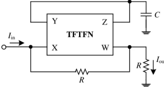
TFTFN Y X Z W Iout R C R Iin
Fig. 7 Tunable current-mode allpass filter
In order to demonstrate the application example of the proposed TFTFN, the tunable current-mode allpass filter as shown in Fig. 7 [12] was simulated. The transfer function of the TFTFN-based allpass filter can be given by
( )
( )
(
(
sRC k)
)
k sRC s I s I + − = 1 1 in out (10) and θd =−2tan−1(
ωRC k)
(11) where θd is the phase angle of the filter.From the circuit configuration as shown in Fig. 7, If we design R = 10kΩ and C = 10nF, this phase shifter was chosen for a 90° phase shift at ω0/2π = 1.59kHz, when k = 1 (IB3 = 0.5mA). Fig. 8 shows the frequency response of the electronically tunable allpass as shown in Fig. 7 for three different values of the external bias current IB3. Fig. 9 shows the simulation result of the current-mode first order allpass filter with k = 1 (IB3 = 0.5mA).
ICCAS2005 JUNE 2-5, KINTEX, Gyeonggi-Do, Korea
Frequency (Hz) 10 100 1.0K 10K 100K -200 -150 -100 -50 -0 Phas e ( d eg .) IB3 = 0.25mA IB3 = 0.5mA IB3 = 1mA
Fig. 8 Simulated results of the phase against the frequency
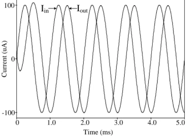
Time (ms) 0 1.0 2.0 3.0 4.0 5.0 -100 0 100 Cu rren t ( u A)
I
inI
outFig. 9 Simulated response of the allpass filter in Fig. 7 3.2 Experimental results and application Example
To verify the performances of the proposed TFTFN, the current mode first order allpass filters as shown in Fig. 7 was implemented using the dual variable OTAs LM13600N with the same circuit parameters used in PSPICE simulation.
I
inI
outFig. 10 Experimental response of the allpass filter in Fig. 7 (vertical scale: 50uA/div, horizontal scale: 400us/div) The experimental result of the current mode of first order allpass filter with k = 1 is shown in Fig. 10. It is evident that
the current mode allpass filter using the proposed FTFN is agreed with the theoretical value.
4. CONCLUSION
In this paper, a simple configuration for the OTA-based FTFN. The proposed circuit comprises only three OTAs. The current gain can be electronically adjusted by the external bias current of the OTAs. Demonstrated simulation and experimental results are used to confirm the basic circuit performances. The implementation of current-mode allpass filter using the proposed FTFN is the application example.
REFERENCES
[1] B.D.H. Tellegen, “La recher pour une serie compleate d’elements de circuit ideaux non-lineires”, in Rendicouti Del Seminario Matematico e Fisico di Milano, Vol. 25, pp. 134-144, Apr. 1954.
[2] H.J. Carlin, “Singular network elements”, IEEE Trans. Circuit Theory, Vol. CT-11, pp. 67-72, Mar. 1964. [3] J.H. Huijsing, “Operational floating amplifier”, IEE
Proceedings, Vol. 137, Pt. G, No. 2, pp. 131- 136, Apr. 1990.
[4] Shen-Iuan Liu, “Cascadable current-mode filters using single FTFN”, Electronics Letters, Vol. 31, No. 23, pp. 1965- 1966, Nov. 1995.
[5] B. Chipipop and W. Surakampontorn, “Realisation of current-mode FTFN-based inverse filter”, Electronics Letters, Vol. 35, No. 9, pp. 690- 692, Apr. 1999. [6] D.R. Bhaskar, “Grounded-capacitor SRCO using only
one PFTFN”, Electronics Letters, Vol. 38, No. 20, pp. 1156-1157, Sep. 2002.
[7] U. Cam, A. Toker and H. Kuntman, “CMOS FTFN realisation based on translinear cells”, Electronics Letters, vol. 36, no. 15, pp. 1255-1256, July. 2000. [8] A. Jiraseri-amornkun, B. Chipipop, and W.
Surakampontorn, “Novel Translinear-based Multi-output FTFN”, The 2001 IEEE International Symposium on Circuits and Systems (ISCAS2001), Vol. 1, pp. 180-183, 6-9 May 2001.
[9] Hussain Alzaher and Mohammed Ismail, “A CMOS Fully Balanced Four-Terminal Floating Nullor”, IEEE Transactions of Circuits and Systems-I, Fundamental Theory and Applications, Vol. 49, No. 4, pp. 413-424, Apr. 2002
[10] Worapong Tangsrirat, Sumalee Unhavanice, Teerasilapa Dumawipata, and Wanlop Surakampontorn, “FTFN with Variable Current Gain”, Proc. of IEEE Region 10 International Conference on Electrical and Electronic Technology (TENCON), Vol. 1, pp. 209-212, 19 –22 Aug. 2001
[11] C.F. Wojslaw, E.A. Moustakas, “Operational Amplifier: the devices and their applicaiton”, New York: John Wiley, 1986.
[12] M. Higashimura, “Current-mode allpass filter using FTFN with grounded capacitor”, Electronics Letters, Vol. 27, No. 13, pp. 1182-1183, 1991.
ICCAS2005 JUNE 2-5, KINTEX, Gyeonggi-Do, Korea