https://doi.org/10.6113/JPE.2019.19.6.1591 ISSN(Print): 1598-2092 / ISSN(Online): 2093-4718
JPE 19-6-25
Practical SPICE Model for IGBT and PiN Diode
Based on Finite Differential Method
Han Cao
*, Puqi Ning
†, Xuhui Wen
*, and Tianshu Yuan
* †,*University of Chinese Academy of Sciences, Beijing, China;Institute of Electrical Engineering, Chinese Academy of Sciences, Beijing, China; Key Laboratory of Power Electronics and Electric Drive,
Institute of Electrical Engineering, Chinese Academy of Sciences, Beijing, China; Collaborative Innovation Center of Electric Vehicles in Beijing, Beijing, China
Abstract
In this paper, a practical SPICE model for an IGBT and a PiN diode is proposed based on the Finite Differential Method (FDM). Other than the conventional Fourier model and the Hefner model, the excess carrier distribution can be accurately solved by a fast FDM in the SPICE simulation tool. In order to improve the accuracy of the SPICE model, the Taguchi method is adopted to calibrate the extracted parameters. This paper presents a numerical modelling approach of an IGBT and a PIN diode, which are also verified by SPICE simulations and experiments.
Key words: Finite differential method, IGBT, Model, PiN diode, SPICE
N
OMENCLATUREA Total die area of a diode (cm2).
i
A Total die area of an IGBT (cm2).
CG C Gate-collector capacitance (nF). dep C Depletion capacitance (nF). GE C Gate-emitter capacitance (nF). ox C Oxide capacitance (nF). res
C Reverse transmission capacitance (nF).
D Ambipolar diffusivity (cm2 /s). n D Electron diffusivity (cm2 /s). p D Hole diffusivity (cm2 /s). si
Dielectric constant of silicon (F/cm).
n
h Electron recombination coefficient (cm4 /s).
p
h Hole recombination coefficient (cm4 /s).
C
I Collector current of an IGBT (A).
CG
I Collector-gate current in an IGBT (A).
D
I Total anode current of a diode (A).
1
disp
I Displacement current atx (A).l
2
disp
I Displacement current atx (A).r
G
I Drive current of an IGBT (A).
GE
I Gate-emitter current in an IGBT (A).
mos
I MOS channel region current (A).
1
n
I Electron current atx (A).l
2
n
I Electron current atx (A).r
1
p
I Hole current atx (A).l
2
p
I Hole current atx (A).r
T
J Current density of a diode (A/cm2).
p
K MOS channel transconductance Ω-1.
B
N Base impurity doping concentration (cm-3).
p Carrier density of drift region (cm-3).
l
p Carrier density atx (cml -3).
r
p Carrier density atx (cmr -3).
base
p Average carrier density of drift region (cm-3).
q Electron charge (c).
t Time (us).
doff
t Turn-off delay time (ns).
don
t Turn-on delay time (ns).
© 2019 KIPE Manuscript receivedDec. 21, 2018; accepted May 29, 2019
Recommended for publication by Associate EditorSang-Won Yoon.
†Corresponding Author: [email protected]
Tel: +86-13269167295, Institute of Electrical, CAS
*University of Chinese Academy of Sciences, Beijing, China; Institute of
Electrical Engineering, Chinese Academy of Sciences, Beijing, China; Key Laboratory of Power Electronics and Electric Drive, Institute of Electrical Engineering, Chinese Academy of Sciences, Beijing, China; Collaborative Innovation Center of Electric Vehicles in Beijing, Beijing, China
HL
High-level lifetime (us).
n Electron mobility (cm/s). p Hole mobility (cm/s). sat v Saturation mobility (cm/s). AK
V Diode voltage drop (V).
CG
V Collector-gate voltage (V).
d
V Depletion region voltage drop (V).
DS
V Drain-source voltage in a MOSFET (V).
GE
V Gate-emitter voltage (V).
GS
V Gate-source voltage in a MOSFET (V).
j
V Junction voltage drop (V).
T
V Thermal voltage (V).
th
V Threshold voltage of a MOSFET (V).
B
W Drift region width of a diode (um).
i
W Drift region width of an IGBT (um).
x
Differential step (um).
l
x Left boundary of drift region (um).
r
x Right boundary of drift region (um).
I. I
NTRODUCTIONAn insulated gate bipolar transistor (IGBT) can be equivalent to a giant transistor (GTR) driven by a metal-oxide semiconductor field effect transistor (MOSFET) in the physical structure. Therefore, it has the advantages of both GTRs and MOSFETs, such as high input impedance and low on-state voltage. With increments in its voltage and current ratings, the application range can be extending from medium power applications to high power applications [1].
The authors of [2] presented a 6.5 kV commercially available IGBT module in a boost circuit application switching at 9 kHz, and a 7 kA IGBT module was fabricated in [3]. Improvements in packing materials and structure design enable IGBTs to be operated at higher frequencies. Thus, the authors of [4] provided an ultra-thin punch-though IGBT with a blocking voltage of 650V, which is able to drive DC-DC converter at 200 kHz.
Since the invention of the first IGBT in 1982 [5], various of modeling methods have been proposed from different aspects and with different objectives. However, depending on the modeling method used, the models can be divided into two categories, numerical models and behavioral models.
Behavioral models concentrate on IGBT behavior without considering their physical mechanism. A curve-fitting method was used in [6] to calculate switching losses. However, this model cannot demonstrate dynamic behavior. The authors of [7] used a Hammerstein model to describe the static characteristics and the switching characteristics of an IGBT.
Fig. 1. Configuration of a Hammerstein model.
The configuration of this model is illustrated in Fig. 1, and the model was simulated with Saber. Although behavioral models can simply and accurately describe IGBTs, they lack universality.
Numerical models refer to analytical models based on semiconductor physics. Solving an Ambipolar Diffusion Equation (ADE) Equ. (1) with different simplifications to obtain excess carriers distribution p(x,t) is the key point of modelling.
(1)
There are three approaches based on this method: (1), Hefner model [8], Fourier-based model [9] and Laplace transformation model [10]. The Hefner model assumes a linear distribution of excess carriers and describes them as Equ. (2). This method is appropriate for a planar IGBT. However, it is not appropriate for a trench-field-stop IGBT and a PIN diode. The Fourier-based model can simulate all kinds of IGBTs. However, its iterations are too complex, which can lead to some problems in terms of convergence. The drift region excess carrier distribution of a Fourier-based model can be calculated by Equ. (3). A Laplace transformation model can solve the ADE in the frequency domain. However, it is not suitable for changes of the drift region boundary.
(2)
(3)
To simplify the calculations and improve accuracy, this paper presents a novel approach to solve Equ. (1) with the Finite Differential Method. In addition, a physical SPICE model for an IGBT and a PIN diode is built in SIMetrix. The simulation is more stable and faster than both the Fourier- based model and the Laplace transformation model. This is due to the simplifications in the drift region and the accurate description of the boundary.
II. S
IMULATION OF THED
RIFTR
EGIONA. Finite Differential Method Implementation in SPICE A time domain based partial differential equation solution was proposed in [11]. According to this method, the drift
2 2 HL p p p D + t x 2 3 0 0 ( , ) [1 ] [ ] 2 6 3 x P x Wx x dW p x t P W WD W dt 1 0 2 1 1 ( ) ( , ) ( ) ( )cos
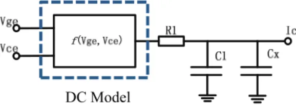
k k k x x p x t v t v t x x DC ModelFig. 2.Method for solving an ADE in a SPICE simulation.
region can be finite differenced in k equal parts, x1, …, xj, …xk. Hence, the orders of the ADE can be reduced by Equ. (4) and Equ. (5) in part j, and the partial differential equation can be simplified as Equ. (6).
(4)
(5)
(6) Equ. (6) can be solved by a SPICE simulation, where it is replaced by a simple network of resistors and capacitors driven by voltage controlled current sources. As showed in Fig. 2, pj is replaced by the node voltage ej, and the differential of pj is equivalent to the charge current of C.
The value chosen for C and R is unimportant as long as the
R-C time constant is much larger than the largest time of the
ADE interest. In addition, a large number (larger than 1015) or
a non-zero small number (less than 10-6) results in convergence
problems in SIMetrix.
Based on this principle, the values of R and C are chosen as 1 and 10-6, respectively. Hypothetically, the drift region is finite
differenced in k equal parts. A higher k can result in a higher calculation accuracy. However, the solving process is more complex and the simulation time increases. Hence, a trade-off between calculation accuracy and simulation speed should be made. As a consequence, the stage number is chosen as 5. Taking the boundary conditions of Equ. (7) and Equ. (8) into consideration, the excess carrier distribution can be calculated by Equ. (9).
(7)
(8)
(9)
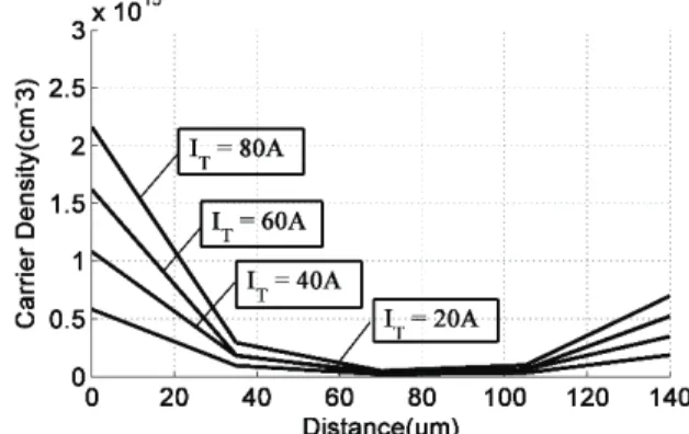
Fig. 3.Carrier distribution of a PiN diode under different .
where:
, , , ,
, ,
B. The Excess Carrier Distribution Simulation
Based on this method, the excess carrier distribution of a PiN diode (IRD3CH53DB6) can be simulated in SIMtrix. In addition, the same method can be used to simulate the drift region distribution of an IGBT. The results are shown in Fig. 3.
The largest concentration of the electrons and holes in the drift region during a turn-on transient occurs at its boundary. The drop in the carrier density towards the center of the drift region is determined by τHL and D. The reduction of the average carrier density into the drift region with a reduction of the injected current IT can be explained by the charge control method [12].
Suppose the recombination of the end regions is neglected. Consequently:
(10)
Where R is the recombination rate, which is given by:
(11)
The average carrier density in the drift region is then described by:
(12)
Due to this relationship, it can be concluded that the average carrier density has a positive correlation with JT and
τHL, which can be verified in Fig. 3.
Bipolar devices mainly work under large injection levels j e , j j j
a e
, 1 1 j j j a e aj j, 1ej1 j j+1 j p p p = x x 2 2 j j+1 j-1 j 2 p p +p 2p x x 1 j j-1 j j+1 2 2 2 HL p D D D p 2 p + p t x x x D disp1 p 2 1 2 1 p I I h p +p + p =0 x x 2qAD D D disp2 2 k k-1 n k n I I p p h + + p =0 x x 2qAD D 1 1 1 11 12 2 2 0 0 0 0 2 21 22 23 2 32 33 34 3 3 43 44 45 4 4 54 55 5 p b u d d 0 p a a a 0 0 p 0 d p = 0 a a a 0 p + 0 dt 0 0 a a a 0 p p 0 0 0 d d p b u T I 11 121 d d x j j, 1 j j, 1 2 D a a x , 1 j j 2 HL D a 2 x 1 1 p p h b 2qAD D 1 n 2 n h b 2qAD D 1 2 D disp1 1 u I -I p T 2 2 D disp2 k u I -I p r T l J = qRdx
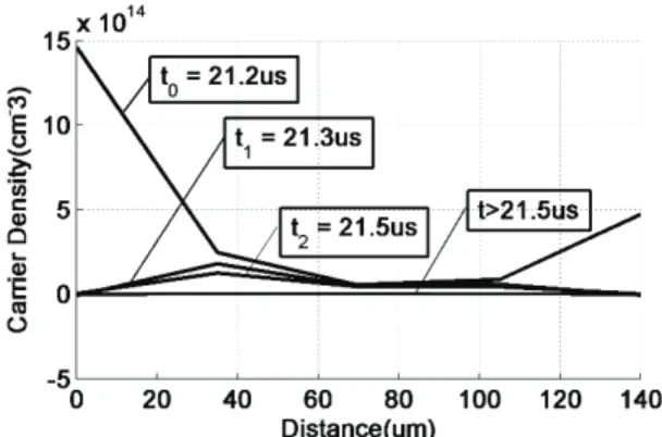
( ) HL n x R ( ) T HL a r l J n q x x Fig. 4.Carrier distribution in the reverse recovery (before 21.5us).
Fig. 5.Carrier distribution in the reverse recovery (after 21.5us).
and their drift region contains a large number of electrons and holes which makes it a low resistance state. When a PiN diode is switched from the conduction mode to the reverse-blocking mode, the excess carrier density of the drift region decreases rapidly due to the termination of the injection. The stored charge within the drift region of the PiN diode must be extracted before it can support high voltages. This process is illustrated in Fig. 4 and Fig. 5. This phenomenon is referred to as reverse recovery.
III. D
IODEM
ODELI
MPLEMENTATIONTo implement the FDM model for a PiN diode, the basic one-dimension diode body is divided into three parts, as shown in Fig. 6. The performance characteristics of the PiN diode depend mainly on the chip geometry and the processed semiconductor material in the drift region [13]. When the PiN diode is forward biased, holes and electrons are injected into the drift region. This charge does not recombine instantaneously. Instead it has a finite lifetime (τHL) in the drift region. If the PiN diode is reverse biased, there is no stored charge in the drift region, which behaves like a parallel
R-C network.
A. Physics Method for PiN Diode Modeling
The on-state voltage drop of a PiN diode VAK consists of three parts, which are the junction voltages Vj, the voltage of the drift region VB and the voltage of the depletion region Vd.
Fig. 6. Physical structure of a PiN diode.
(13)
Neglecting the distributional effects in the drift region, Vj and Vd can be described by a simple quasi-static model as Equ. (14) and Equ. (15). The voltages across the P+/N- junction and the N+/N- junction are determined by the injected minority carrier density and the majority carrier density, respectively. More importantly, Equ. (14) can be derived under the charge neutrality condition p(x)=n(x).
In Equ. (15), Ip1/Avsat and In1/Avsat are far less than qNB. Consequently, neglecting them can improve the calculating speed and the convergence property of the FDM model.
(14)
(15)
(16)
B. PiN Diode Parameters Extraction
The first parameter that needs to be extraction is the chip area A, which is closely related to the rated current. The approach to extract A is to directly measure the diode area or to obtain it from a datasheet.
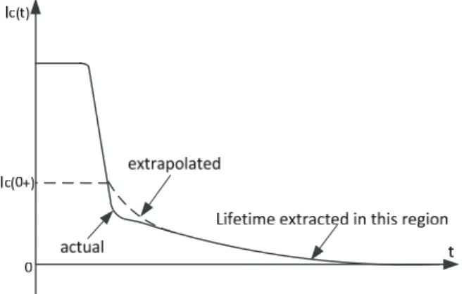
The parameter τHL must be determined from the diode turn-off waveform such as the one shown in Fig. 7. Under this circumstance, τHL can be calculated by Equ. (17) [14].
(17)
Where α is the current slope from T0 to T1. T0 is the zero-crossing point during the turn-off transient, and T1 is the moment the reverse recovery current reaches its peak value.
τrr is the reverse recovery time constant, which can be
measured from the current waveform.
Another important parameter is the drift region width Wd, which can influence the breakdown voltage of bipolar semiconductor devices. The approach to extracting Wd is based on Equ. (18) [15], and the PiN diode parameters extraction results are listed in Table I.
(18)
Where VBR is the avalanche breakdown voltage. In addition,
a and b represent two constants that are related to the
semiconductor technology. AK j B d V V V V 2 ln r l j T i p p V V n 1/ 2 2/ ( )2 2 2 B p sat B n sat d l B r si si qN I Av qN I Av V x W x 2 ln ( ) p r l D r B T n B n p base n p l D x x I p V V Aq N p D D p 1 exp( ) RM rr T I = ln( ) B BR B bW V aW
Fig. 7. Turn-off waveform of a PiN diode. TABLE I
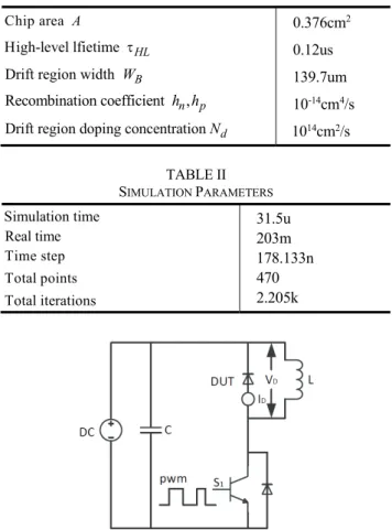
PARAMETERS EXTRACTION RESULTS OF A DIODE 0.376cm2 0.12us 139.7um 10-14cm4/s 1014cm2/s TABLE II SIMULATION PARAMETERS 31.5u 203m 178.133n 470 2.205k
Fig. 8. Double-pulse test with the proposed diode model.
C. PiN Diode Model Verification
With all of the above equations, the PiN diode model is simulated in SIMetrix. SIMetrix is a mixed-signal circuit simulator with its core algorithms based on the SPICE program. The simulation parameters are listed in Table II.
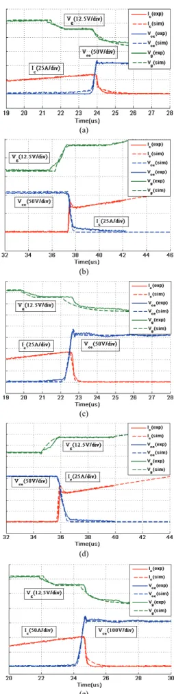
To verify the simulation results of SIMetrix, a double- pulse test circuit was developed as shown in Fig. 8, and the DUT (Device Under Test) is an IRD3CH53DB6. A 42.3 mH inductor served as a load and the value of the driver resistance Rg was chosen as 7.5 Ω. In order to avoid the
(a)
(b)
Fig. 9. Double-pulse test with the proposed PiN model (Vgon=15V, Vgoff=-9V, Rg=7.5Ω, L= 42.3 mH). (a) Under a DC bus voltage of 100V. (b) Under a DC bus voltage of 200V.
Fig. 10. Physical structure of an IGBT.
spurious triggering caused by the Miller capacitance, Vgoff was set at -9 V. Fig. 9 shows a comparison of simulation and experimental results.
IV. IGBT
M
ODELI
MPLEMENTATIONThe basic unit cell structure of an IGBT is shown in Fig. 10. The N+ zone is called the source region, and the electrode attached to it is called the source electrode. The N plus area is called the drift region. The control area of the IGBT is the gate area, and the channel is formed near the boundary of the gate.
A. Physics Method for IGBT Modeling
The basic IGBT dynamic model consists of three state equations: the current continuity equation, the voltage drop equations and the IGBT driver equations. The current continuity equation governing the behavior of IGBT is describe as Equ. (19).
(19)
Where In1=qAihppl2, In2=Imos and the specific descriptions of
Idisp2 and ICG are described in [16].
Chip area A
igh-level lfietime HL
Drift region width WB
Recombination coefficient ,h hn p Drift region doping concentrationNd
Simulation time Real time Time step Total points Total iterations 1 1 2 2 2 C n p n p disp CG I I I I I I I
Fig. 11. Typical IGBT application circuit.
Fig. 12. Equivalent circuit of Miller capacitance.
The voltage drop of an IGBT is comprised of three parts: the voltage across the junctions J1, the voltage across the depletion region Vd2, and the voltage across the drift region VB. Similarly, the three voltages can be describe as Equ. (20), Equ. (21) and Equ. (22).
(20)
(21)
(22)
A typical IGBT application circuit is illustrated in Fig. 11. According to Kirchhoff’s law, the current flowing into the gate terminal is equal to the current flowing out of it. Consequently, IG and ICG can be described as Equ. (23) and Equ. (24), respectively. Combining Equ. (23) with Equ. (24), the IGBT driver equation is derived as Equ. (25). The MOS part of the IGBT can be directly implemented with a PSPICE MOSFET model.
(23)
(24)
(25)
B. Miller Plateau Implementation
The Miller plateau caused by Miller capacitance can lead to a loss of control over the turn-on di/dt [17] and snap-off
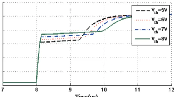
Fig. 13. Miller plateau characteristics with values of different Vth.
Fig. 14. Miller plateau characteristics with different values of CJO.
Fig. 15. Miller plateau implementation.
during the turn-off process, which can result in device failures. The Miller capacitance forms from an overlap of the gate metallization and the N-drift region [18]. It can be described as a voltage-controlled capacitance that is not available for SPICE simulations.
In this paper, voltage-controlled current sources are used to simulate the charge process of ICG. The moment the Miller Plateau occurs is related to the threshold voltage of the elemental MOSFET. This phenomenon is shown in Fig. 13.
In this method, Cox and Cdep are equivalent to CAP and DCAP, respectively. By changing the null-bias capacitance CJO and the junction electric potential VJ of the DCAP, different Miller plateau characteristics can be simulated, as shown in Fig. 14. In addition, Fig. 15 shows a comparison of simulation and experimental results, under the same condition with the diode test.
C. IGBT Parameters Extraction
The parameters that need to be extracted for the modeling
ln l j1 T i p V 2V n 2 2/ ( ) 2 B n i sat d2 i r si qN I Av V W x 2 ln ( ) p r l r B T i n B n p base n p l D x x Ic p V V A q N p D D p CG GE G CG GE CGdV GEdV I I +I =C +C dt dt ( CE GE) CG CG dV dV I =C dt dt GE G CG CE GE CG GE CG dV I C dV = dt C C C C dt
Fig. 16. Current tail of an IGBT.
of an IGBT can be divided into five categories: the MOS part parameters, IGBT structure parameters, IGBT drift region parameters, IGBT lifetime parameters and IGBT recombination coefficients.
The structure parameters include the device area and the oxide capacitance Cox of the IGBT. The device area can be measured or obtained directly from a datasheet. The oxide capacitance is a part of the Miller capacitance. It can be acquired from the Cres curve in the datasheet. When Cres reaches its maximum value, the depletion layer has not
formed yet ( ). This means the value of Cox is the
same as Cres.
Other than the PiN diode, the drift region parameter Wi is different between Non-Punch Through (NPT) IGBTs and Punch Through (PT)/Field Stop (FS) IGBTs. Since the electric field in the drift region of an NPT IGBT is a triangular distribution, Wi can be derived by Equ. (26). As for a PT/FS IGBT, the electric field of the drift region is a trapezoidal distribution, and the drift region width of the IGBT can be calculated by Equ. (27).
(26)
(27)
Where Ec is the typical value of the silicon-based electric field, and VBR is the avalanche breakdown voltage of the IGBT.
In order to extract a high-level lifetime τHL of the IGBT, the current tail in the turn-off transient under an inductive load needs to be measured. According to the method in [19], τHL is the time constant of the current tail as shown in Fig. 16.
The MOS part of the IGBT can be directly implemented with a PSPICE MOSFET model, the parameters of which
include the MOSFET threshold voltage Vt h and
transconductance Kp. Vth is the threshold voltage of the MOSFET which means the gate voltage at the critical conduction moment. Kp is the channel transconductance of the MOSFET, which represents the ability of the gate voltage
TABLE III
PARAMETERS EXTRACTION RESULTS OF AN IGBT 0.376cm2 11.9n 0.12us 125.7um 5.3V 13.2AV-2 10-14cm4/s 1014cm2/s TABLE IV L9(34)ORTHOGONAL TABLE # 1 4.7 12.0 10.6 111.7 2 5.3 13.2 11.9 125.7 3 5.9 14.4 13.2 139.7
to control the collector current. These two parameters can be extracted from Equ. (28), and the IGBT parameters extraction results are listed in Table III.
(28) D. Taguchi Method for Calibration
Due to measurement error, the extracted parameters cannot be completely accurate. Consequently, the Taguchi method was adopted to calibrate the model based on the FDM. The Taguchi method is a statistical method, developed by Genichi Taguchi to improve the quality of manufactured goods. More recently, it has been applied to engineering [20].
In the Taguchi method, quantitative indexes are designed to compare the losses of different experimental groups. The purpose of the FDM model is to simulate the switching performances of an IGBT. As a result, a Taguchi loss function is designed as Equ. (29).
The calibration parameters are the threshold voltage Vth, transconductance Kp, oxide capacitance Cox and drift region width of the IGBT Wi. The extracted parameters are taken as median values. The threshold values are generated by 90% and 110% of median values, respectively. A L9 (34) orthogonal
table is set as shown in Table IV, and the results of Taguchi experiments are displayed in Table V. Calibration results of the Taguchi method are illustrated in Fig. 17.
(29) i A dep C = si c i B E W qN 2 ( 2 / ) si i B c c B BR si W qN E E qN V Chip area Ai
Oxide capacitance Cox
igh-level lfietime HL
Drift region width Wi
Threshold voltage Vth Transconductance Kp
Recombination coefficient ,h hn p Drift region doping concentration NB
th V Kp Cox Wi 2 2 ( ) 2 ( ) 2 DS p GS th DS DS GS th mos p GS th V K V V V for V V V I K V V otherwise 2 2 2
_ exp _ exp _ exp
_ exp _ exp _ exp
r r don don doff doff
loss r don doff t t t t t t E t t t 2 _ exp _ exp f f f t t t
No 1 1 1 1 1 0.065 2 1 2 2 2 0.062 3 1 3 3 3 0.075 4 2 1 2 3 0.014 5 2 2 3 1 0.051 6 2 3 1 2 0.104 7 3 1 3 2 0.008 8 3 2 1 3 0.046 9 3 3 2 1 0.086 K1 0.202 0.087 0.214 0.201 K2 0.169 0.159 0.163 0.175 K3 0.139 0.265 0.134 0.135 *
Fig. 17. Calibration results of the Taguchi method.
Fig. 18. Double-pulse test with the proposed IGBT model.
E. IGBT Model Verification
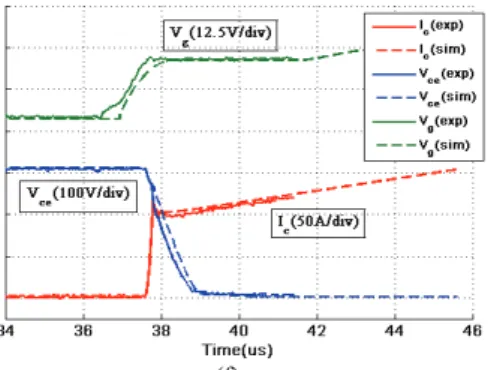
With all of the above equations and parameters, an IGBT model is simulated in SIMetrix. The simulation conditions are the same as those of the PiN diode. To verify the simulation results of the SIMetrix, a double-pulse test circuit was developed to compare the switching transients and the Miller plateau with the simulation results as shown in Fig. 18. The DUT (Device Under Test) is an IRG8CH97K10F. Fig. 19 illustrates the switching transients of the proposed IGBT.
(a) (b) (c) (d) (e) th V Kp Cox Wi Eloss 3 th V Kp1 Cox3 Wi3
(f)
Fig. 19. Switch transients of the proposed IGBT (Vgon=15V, Vgoff=-9V, Rg=7.5Ω, L= 42.3 uH). (a) Turn-off transient under a DC bus voltage of 100V. (b) Turn-on transient under a DC bus voltage of 100V. (c) Turn-off transient under a DC bus voltage of 200V. (d) Turn-on transient under a DC bus voltage of 200V. (e) Turn-off transient under a DC bus voltage of 300V. (f) turn-on transient under a DC bus voltage of 300V.
V. C
ONCLUSIONSThis paper proposes a practical SPICE model for an IGBT and a PiN diode based on Finite Differential Method. The model relates well to experiment results during turn-on and turn-off transients. The Miller plateau and reverse characteristics of the PiN diode are also included. The key point of this modeling is to solve the Ambipolar Diffusion Equation in a SPICE simulation. Taking into account the charge dynamics within the base region of the device, the presented model provides great improvements in terms of model speed and accuracy.
A
PPENDIXThe FDM part of the IGBT SPICE model proposed in this paper is: ************************************************** *************** Differential Coefficients ************ ************************************************** .PARAM C11 = {((N-1)/Wd)**2*D*1.0E2} .PARAM C12 = {-2*C11-1/Td} .PARAM C13 = {C11} .PARAM E11 = {-(N-1)/Wd} .PARAM E12 = {-E11}
.PARAM E13 = {1/(2*q*Ad*Dp)*1E-16} .PARAM E14 = {-hp*1E8/D}
.PARAM E15 = {1/(2*q*Ad*Dn)*1E-16}
************************************************** ***************** FDM Part of IGBT *************** ************************************************** R1 1 12 RX
G1 12 1 POLY(3) 1 12 2 12 14 12 0 E11 E12 E13 E14
R2 2 12 RX C2 2 12 CX IC = 0 BRANCH={IF(ANALYSIS=2,1,12)} G2 12 2 POLY(3) 1 12 2 12 3 12 0 C11 C12 C13 R3 3 12 RX C3 3 12 CX IC = 0 BRANCH={IF(ANALYSIS=2,1,12)} G3 12 3 POLY(3) 2 12 3 12 4 12 0 C11 C12 C13 R4 4 12 RX C4 4 12 CX IC = 0 BRANCH={IF(ANALYSIS=2,1,12)} G4 12 4 POLY(3) 3 12 4 12 5 12 0 C11 C12 C13 R5 5 12 RX
G5 12 5 POLY(3) 5 12 4 12 15 12 0 E11 E12 E15 E14
************************************************** ***************** Voltage of IGBT***** *********** ************************************************** EJ1 11 103
VALUE ={LIMIT( 2*VT*LN(V(1,12)/(ni/1e12) ) ,0,10)} EJ2 103 104
VALUE = {LIMIT(V(14,12) *0.6E5/(1.4E5 +
1850/N*(V(1,12)+V(2,12)+V(3,12)+V(4,12)+V(5,12)))+2*VT *Dp/(Dn+Dp)*LN(V(5,12)/V(1,12)+10),0,10)} EJ3 104 105 VALUE = {V(202,12)} ************************************************** ***************** Current of IGBT***** *********** ************************************************** EP1 14 12 VALUE={I(EJ1)} RP1 14 12 1 EP2 15 12 VALUE={I(EJ1)} RP2 15 12 1
A
CKNOWLEDGMENTThiswork is supported by The National key research and development program of China (2016YFB0100600), the Key Program of Bureau of Frontier Sciences and Education, Chinese Academy of Sciences (QYZDBSSW-JSC044).
R
EFERENCES[1] K. Sheng, B. W. Williams, and S. J. Finney, “A review of IGBT models,” IEEE Trans. Power Electron., Vol. 15, No. 6, pp. 1250-1266, Nov. 2000.
[2] S. Castagno, R. D. Curry, and E. Loree, “Analysis and comparison of a fast turn-on series IGBT stack and high- voltage-rated commercial IGBTS,” IEEE Trans. Plasma Sci., Vol. 34, No. 5, pp. 1692-1696, Oct. 2006.
[3] Q. Al'Akayshee, A. Sartain, A. Golland, F. Wakeman, M. Talebinejad, and A. D .C. Chan, “Press pack IGBT: High current pulse switch transcranial magnetic simulation,” IET Int. Conference on Power Electronics, 2014.
[4] H. Chang, J. Bu, G. Kong, and R. Bou, “High speed 650V IGBTs for DC-DC conversion up to 200 kHz,” IEEE Int.
[5] B. J. Baliga, M. S. Adler, P. V. Gray, R. P. Love, and N. Zommer, “The insulated gate rectifier (IGR): A new power switching device,” International Electron Devices Meeting, 2005.
[6] E. S. Kim, K. Y. Joe, M. H. Kye, Y. H. Kim, and B. D. Yoon, “An improved soft-switching PWM FB DC/DC converter for reducing conduction losses,” IEEE Trans. Power Electron., Vol. 14, No. 2, pp. 258-264, Mar. 1999. [7] J. T. Hsu and K. D. T. Ngo, “Behavioral modeling of the
IGBT using the Hammerstein configuration,” IEEE Trans. Power Electron., Vol. 11, No. 6, pp. 746-754, Nov. 1996. [8] A. R. Hefner, “An improved understanding for the transient
operation of the power insulated gate bipolar transistor (IGBT),” IEEE Trans. Power Electron., Vol. 5, No. 4, pp. 459-468, Oct. 1990.
[9] P. Leturcq, M. O. Berraies, and J. L. Massol, “Implementation and validation of a new diode model for circuit simulation,” Pesc Record IEEE Power Electronics Specialists Conference. IEEE., pp. 35-43, 1996.
[10] A. G. M. Strollo and D. De Caro, “Low power flip-flop with clock gating on master and slave latches,” Electronics Letters., Vol. 36, No. 4, pp. 294-295, Feb. 1990.
[11] W. R. Zimmerman, “Time domain solutions to partial differential equations using SPICE,” IEEE Trans. Edu., Vol. 39, No. 4, pp. 563-573, Nov. 1996.
[12] B. Baliga, Fundamentals of Power Semiconductor Devices, Science Press, Chap. 2, 2008.
[13] R. H. Caverly and S. Khan, “Electrothermal modeling of microwave and RF PIN Diode switch and attenuator circuits,” IEEE International Microwave Symposium Digest., pp. 1-4, 2013.
[14] A. Barna and D. Horelick, “A simple diode model including conductivity modulation,” IEEE Trans. Circuit Theory, Vol. 18, No. 2, pp. 233-240, Mar. 1971.
[15] M. J. Declercq and J. D. Plummer, “Avalanche breakdown in high-voltage D-MOS devices,” IEEE Trans. Electron. Dev., Vol. 23, No. 1, pp. 1-4, Jan. 1976.
[16] A. R. Hefner, “Device models, circuit simulation, and computer-controlled measurements for the IGBT,” IEEE Workshop on Computers in Power Electronics., pp. 5-7, 1990.
[17] Y. Teng, J. Tan, Q. Yu, and Y. Zhu, “Analysis of the negative Miller capacitance during switching transients of IGBTs,” Tencon IEEE Region 10 Conference., pp. 1-4, 2015.
[18] J. Boehmer, J. Schumann, and H. G. Eckel, “Effect of the miller-capacitance during switching transients of IGBT and MOSFET,” Power Electronics & Motion Control Conference, IEEE., pp. LS6d.3-1 - LS6d.3-5, 2012.
power insulated-gate bipolar transistor,” Solid State Electronics., Vol. 31, No. 10, pp. 1513-1532, Oct. 1988. [20] A. Erfani, M. Muhammadi, S. Asgari Neshat, M. M.
Shalchi, and F. Varaminian, “Investigation of aluminum primary batteries based on taguchi method,” Energy Technology & Policy., pp. 19-27, 2015.
Han Cao was born in Hubei, China. He
received his B.S. degree in Electrical Engineering from Harbin Engineering University, Harbin, China, in 2016. He is presently working towards his Ph.D. degree at the Institute of Electrical Engineering, Chinese Academy of Sciences, Beijing, China. His current research interests include power device modeling and high-density converter designs.
Puqi Ning received his Ph.D. degree in
Electrical Engineering from the Virginia Polytechnic Institute and State University, Blacksburg, VA, USA, in 2010. He is presently working as a Full Professor at the Institute of Electrical Engineering, Chinese Academy of Sciences, Beijing, China. His current research interests include high temperature packaging and high-density converter designs.
Xuhui Wen received her B.S., M.S. and
Ph.D. degrees in Electrical Engineering from Tsinghua University, Beijing, China, in 1984, 1989 and 1993, respectively. She is presently working as a Full Professor at the Institute of Electrical Engineering, Chinese Academy of Sciences, Beijing, China. Her current research interests include high power density electrical drives and generation, especially for electric vehicle applications.
Tianshu Yuan was born in Hefei, China.
He received his B.S. degree in Electrical Engineering from Shandong University, Jinan, China, in 2017. He is presently working towards his M.S. degree at the Institute of Electrical Engineering, Chinese Academy of Sciences, Beijing, China. His current research interests include power device modeling and high-density converter designs.