15-4 / T. J. Park
• IMID 2009 DIGEST
Abstract
We report the multiple quantum well (MQW) structure for highly efficient red phosphorescent OLEDs. Various triplet quantum well devices from a single well to five quantum wells are realized using a wide band-gap hole and electron transporting layers, narrow band-gap host and dopant material, and charge control layers (CCL). The maximum external quantum efficiency of 14.8 % with a two quantum well device structure is obtained, which is the highest value among the red phosphorescent OLEDs using same dopant.
1. Introduction
Organic light emitting diodes (OLEDs) have attracted considerable attention because of their potential applicability to flat-panel displays (FPDs) [1-3] and next generation lighting [4,5]. Several attributes like efficiency, lifetime, driving voltage, and voltage increase during operation should be acceptable for the commercialization of OLEDs. Among of them, the efficiency is the most crucial parameter because it determines the device power and stability. In order to achieve high efficiency in OLEDs, various approaches such as use of highly efficient organic materials, inserting the excition blocking layer and/or hole and electron blocking layers, and optimization of the doping concentration of OLEDs to reduce self-quenching have been reported [6-8]. Among these approaches, especially excition confinement approach by inserting a carrier and/or exciton blocking layer(s) is the most effective and mainly used until now.
In inorganic LED, quantum confinement approach using the multiple quantum well (MQW) structure or multi-quantum barrier leads to a higher efficiency compared to the double hetero-structure or single quantum well (QW) structure. In OLEDs, only few reports about MQW structure with good carrier
confinement ability are presented. Yong Qiu et al. [9,10] have reported the organic MQW structure by using copper phthalocyanine (CuPc) and N, N’-bis(1-naphthyl)-N,N’-diphenyl-1,1’ biphenyl 4, 4’-diamine (NPB) or rubrene. In this paper, the MQW effect has been reported in the fluorescent device, however, real device efficiency is not so high and emission colors aren’t stable [11]. The triplet quantum well structure has reported by S. H. Kim et al. using 4,4’-bis(N-carbazolyl)-1,10-biphenyl (CBP) and PH1 host [12]. Since Ir(ppy)3 is doped in all quantum well layers,
charge carriers can’t be confined effectively if carriers move via dopant molecules. Consequently, high efficiency results have been reported in single QW while they couldn’t get stable high efficiency in MQW structure.
In this study, we report the real MQW device structure having various triplet quantum well devices from a single well to five quantum wells. As the triplet energy in our MQW device is confined at the emitting layers, the highest phosphorescent efficiency is obtained among the Ir(piq)3 dopant PHOLEDs and
color is also very stable.
2. Experimental
The MQW structure is realized using the wide band-gap hole and electron transporting layers, narrow band-gap host and dopant material, and charge control layers (CCL). In a previous article [13], we demonstrated that the red PHOLEDs using tris(1-phenylisoquinoline)irid- ium [Ir(piq)3] dopants and
bis(10-hydroxybenzo[h]- quinolinato) beryllium complex (Bebq2) host material.
Figure 1 shows the structure and energy band diagram of fabricated red PHOLEDs with MQW structure. The emission layer structures of the PHOLEDs were increased by adding the R-EL unit
High efficiency multiple quantum well device structure
in red phosphorescent OLEDs
Tae Jin Park
1, Woo Sik Jeon
1, Jin Jang
1, Ramchandra Pode
2and
Jang Hyuk Kwon
11Department of Information Display and 2Department of Physics, Kyung Hee University,
Dongdaemoon-gu, Seoul 130-701, Korea
Tel.:82-2-961-0948, E-mail: [email protected]
15-4 / T. J. Park
IMID 2009 DIGEST •
[Bebq2: Ir(piq)3/CCL = n, n=1~5]. In order to confine
and control a hole and electron in the EML, we inserted the CCL between red EML. Next, bis[2-(2-hydroxyphenyl)-pyridine] beryllium (Bepp2) hole and
exciton blocking buffer layer is deposited, followed by a 10 % Cs2CO3-doped Bepp2 electron transport
layer (ETL). Then, Al was deposited in another deposition section without breaking vacuum. Deposition rate of Al was 5 ~ 10 Å/sec.
Fig.1. Structure and energy band diagram of fabricated red PHOLEDs with multiple quantum well structure.
The devices were fabricated on ITO coated glass with a sheet resistance of 20 Ω/□. The substrate was cleaned with acetone and isopropyl alcohol sequentially, rinsed in de-ionized water, and then treated in UV-ozone immediately before loading into a high vacuum chamber (~ 2 × 10⁻⁷ Torr). The current
density-voltage (J–V) and luminance–voltage (L–V) data of red PHOLEDs were measured by Keithley 2635 A and Minolta CS-1000A, respectively. The red PHOLED area was 2 mm2 for all the samples studied
in the present work.
3. Results and discussion
In order to select the best CCL, we fabricated red PHOLEDs (n=2) with different CCL (CBP; device B, TCTA; device C, Bepp2; device D) at the fixed CCL
thickness of 5 nm. Device A was made without CCL. Figure 2 shows the J-V characteristics of fabricated red PHOLEDs without and with CCL. The inset of Figure 2 shows the external quantum efficiency (EQE) characteristics of device A~D. All four devices were measured until 10,000 cd/m2 brightness value. The
current densities (at 5 V) of the device A, B, C and D are 90.3 mA/cm2, 10.2 mA/cm2, 5.1 and 26.3 mA/cm2,
respectively. As expected, the current density increases with the increasing number of R-EL units. At a given constant luminance of 1000 cd/m2, the
EQE are 10.8 % for single well device, 5.1 % for the device B, 5.2 % for the device C, and 13.8 % for the device D, respectively. The EQE of device D with Bepp2 CCL is significantly higher than those of device
A~C.
Fig.2. J-V characteristics of fabricated single quantum well device and double quantum well devices with different CCL. The inset shows the external quantum efficiency (EQE) characteristics of device A~D.
The lowest unoccupied molecular orbital (LUMO) levels of CBP, TCTA and Bepp2 CCL were at 2.6 eV,
2.4 eV, and 2.6 eV, respectively. While the highest occupied molecular orbital (HOMO) levels of CBP, TCTA and Bepp2 CCL were at 5.9 eV, 5.8 eV and 5.7
eV, respectively. Therefore, CBP and TCTA CCL blocked mostly holes and elcetrons at the Bebq2:Ir(piq)3/CCL interface. However, Bepp2 CCL
has suitable LUMO level, so that it can be control the holes and electrons transporting. As a result, Bepp2
CCL confines holes and electrons at the first EML and some of the holes and electrons arrive at the second EML after transporting through the Bebq2 CCL. It is
found that the Bepp2 CCL creates more excitons to be
generated and confined in the double QW EML. Therefore, the device D with the Bepp2 CCL
improved the recombination efficiency of the electron-hole pairs in the emission zone.
15-4 / T. J. Park
• IMID 2009 DIGEST
are probably a dominant factor to control the current flow as hole barriers between HOMO levels of dopant and CCL are relatively high compared with electron barriers. Usually electrons easily overcome its barriers. Further to investigate the influence of the quantum wells on the device performance, if any, we have fabricated PHOLEDs with MQW from 1 to 5 wells.
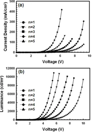
Fig. 3. J-V-L characteristics of fabricated red PHOLEDs with increasing R-EL unit from 1 to 5 : (a) current density-voltage, (b) luminance-voltage
Figure 3 shows the J-V-L characteristics of fabricated red PHOLEDs with the number of R-EL units from 1 to 5. All three devices were measured until 10,000 cd/m2 brightness value. The turn on
voltages of MQW red PHOLEDs are 2.4 V for n=1, 2.5 V for n=2, 2.6 V for n=3, 2.8 V for n=4, and 3.2 V for n=5, respectively. The driving voltage for n=1 to reach 1000 cd/m2 is 3.8 V, 4.2 V for n=2, 4.5 V for
n=3, 3.3 V for n=4, and 3.3 V for n=5. The operating voltages of MQW structure were increased by adding the R-EL unit in the EML. Because of any addition of QW units offers additional resistance to the
conduction of current.
Fig. 4. EQE and power efficiency characteristics of fabricated five red PHOLEDs with increasing R-EL unit from 1 to 5.
Figure 4 shows power efficiency and EQE characteristics of fabricated red PHOLED with MQW from 1 to 5 wells. The maximum EQE values are 11.8 % for n=1, 14.8 % for n=2, 13.6 % for n=3, 12.8 % for n=4, and 8.6 % for n=5, respectively. The maximum power efficiencies are 11.4 lm/W for n=1, 15.4 lm/W for n=2, 13.6 lm/W for n=3, 13.4 lm/W for n=4, and 7.4 lm/W for n=5, respectively. The best EL performance is obtained in n=2 among the five red PHOLEDs with MQW structure.
TABLE 1. Summary of performances of multiple quantum well red PHOLEDs (n=1~5).
n=1 n=2 n=3 n=4 n=5 Operating voltage (1000 cd/m2) 3.8 V 4.2 V 4.8 V 6.0 V 7.4 V Power efficiency (maximum) 11.4 lm/W lm/W 15.4 lm/W 13.6 lm/W 13.4 lm/W 7.4 EQE (%) (maximum) 11.8 % 14.8 % 13.6 % 12.8 % 8.6 % CIE (x, y) (1000 cd/m2) 0.66,0.33 0.66,0.33 0.66,0.33 0.66,0.33 0.66,0.33
The best EL performances are obtained in n=2 as listed in Table 1. These results may be explained that the most excitons can be confined in first and second QWs. Therefore, the best EL performances seem to be
15-4 / T. J. Park
IMID 2009 DIGEST •
obtained with n=2. By increasing the number of quantum wells to n=3 and n=4, the efficiency drop is not significant because electrons can reach to first and second QWs due to the negligible barrier to electron transport. However, the operating voltage is enhanced with increasing the number of QW structures and eventually 5 QW structure does not work properly. In our MQW devices, all devices show excellent color stability with the same CIE coordinate as (0.66, 033) as shown Table I. Our results reveal that the MQW structure improves the external quantum efficiency with no change in the CIE coordinate of red emitting PHOLEDs.
4. Summary
In summary, we propose a multiple quantum well structure with a wide band-gap hole and an electron transporting layers, Bebq2 narrow band-gap host and
Ir(piq)3 red dopant materials, and Bepp2 CCL. Triplet
energies in fabricated MQW devices are confined at the emitting layers. The MQW structure with Bepp2
CCL improved the current and power efficiency. High EQE and power efficiency values of 14.8 % and 15.4 lm/W in a double quantum well structure red PHOLEDs with Bepp2 CCL. It is noted that the MQW
structure is good structure to confine the exciton and improve the recombination efficiency of the electron-hole pairs in the emission zone. This MQW device concept will be very useful to future OLED display and lighting applications.
Acknowledgement
This research was supported by the Ministry of Commerce, Industry and Energy of Korean government.
5. References
1. J. R. Sheats, H. Antoniadis, M. Hueschen, W. Leonard, J. Miller, R. Moon, D. Roitman, and A. Stocking, Science 273, 884-888 (1996).
2. Z. Shen, P. E. Burrows, V. Bulovic, S. R. Forrest, and M. E. Thompson, Science 276, 2009 (1997).
3. R. H. Friend, R. W. Gymer, A. B. Holmes, J. H. Burroughes, R. N. Marks, C. Taliani, D. D. C. Bradley, D. A. Dos Santos, J. L. Bredas, M. Logdlund, and W. R. Salaneck, Nature (London)
397, 121-128 (1999).
4. P. Destruel, P. Jolinat, R. Clergereaux, and J. Farenc,
J. Appl. Phys. 85, 397-400 (1999).
5. B. W. D’Andrade and S. R. Forrest, Adv. Mater. (Weinheim, Ger.) 16, 1585-1595 (2004).
6. V. Bulovic, V. B. Khalfin, G. Gu, and P. E. Burrows, Phys. Rev. B 58, 3730-3740 (1998).
7. M. A. Baldo, D. F. O’Brien, Y. You, A. Shoustikov, S. Sibley, M. E. Thompson, and S. R. Thompson, Nature (London) 395, 151-154 (1998).
8. M. A. Baldo, S. Lamansky, P. E. Burrows, M. E. Thompson, and S. R. Forrest, Appl. Phys. Lett. 75,
4-6 (1999).
9. Y. Qiu, Y. Gao, P. Wei, and L. Wang, Appl. Phys. Lett. 80, 2628-2630 (2002).
10. Y. Qiu, Y. Gao, L. Wang, P. Wei, L. Duan, D. Zhang, and G. Dong, Appl. Phys. Lett. 81,
3540-3542 (2002).
11. J. Huang, K. Yang, S. Liu, and H. Jiang Appl. Phys. Lett. 77, 1750-1752 (2000).
12. S. H. Kim, J. S. Jang, J. M. Hong, and J. Y. Lee, Appl. Phys. Lett. 90, 173501-1-173501-3 ( 2007).
13. T. J. Park, W. S. Jeon, J. J. Park, S. Y. Kim, Y. K. Lee, J. Jang, J. H. Kwon, and R. Pode, Appl. Phys. Lett. 92, 113308-1-113308-3 (2008).