P1-63 / W. H. Park
• IMID 2009 DIGEST
Abstract
A negative waveform having inverted polarity of conventional waveform during reset and sustain periods was proposed to improve the driving characteristics. In order to control the negative wall-charge distribution, a positive bias on the scan electrode was applied during reset period. Compared to 0 V scan-bias condition, at 8 V scan-bias the formative time lag was improved about 23.95 % and the average time lag was improved about 14.91 %. All experiments were performed with the 42-inch PDP module in XGA resolution.
1. Introduction
In display devices, the resolution of an image is one of the important factors that decide an image quality. As demands for the display devices with full HD resolution are growing, many researches on high resolution display have been performed.
The plasma display panel (hereinafter “PDP”) was one of the promising technologies for large area flat-panel displays [1, 2]. The ADS (Address Display Separated) driving method is considered to be the most suitable scheme for stably driving ac PDPs. However, it is still inescapable from the problem that the sustain period decreases as the necessary address period increases.
A negative waveform having inverted polarity of conventional waveform during reset and sustain periods was proposed to improve the high speed driving characteristics in ac PDP [3-6]. A bias voltage on scan electrode (hereinafter “scan-bias”) was applied during reset period to improve the time lag of address discharge. Without the positive scan-bias, the negative charges were accumulated on the scan and address electrodes during reset period. The remained negative charges on the address electrode could be degraded the addressing characteristics. Therefore, with the proper positive scan-bias, the amount of
negative charges on the address electrode could be reduced. All experiments were performed with the 42-in. conventional PDP module and to evaluate the address characteristics the discharge time lags were measured.
2. Experimental Set-up
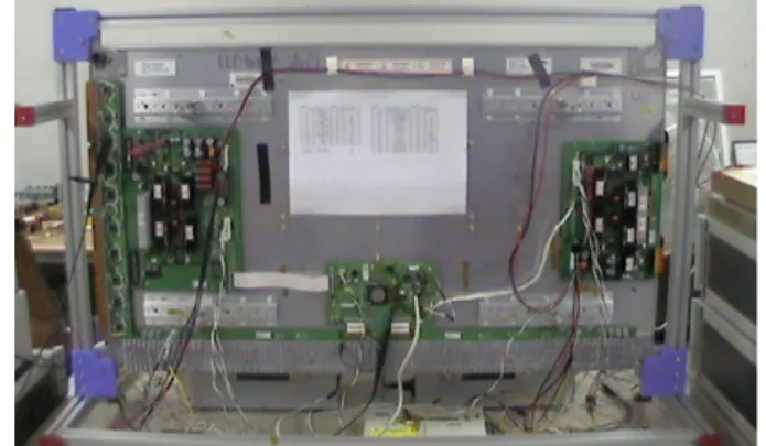
Figure 1 showed the backside of 42-in. tested PDP module in XGA resolution. The reset pulse was applied to X (= sustain) electrode and the scan-bias voltage was applied to Y (= scan) electrode during ramp-up period.
Fig. 1. 42-inch tested PDP module with the negative waveform driving board.
The voltages applied to the test panel were shown in Table 1. During experiments all voltages were fixed except the scan-bias.
Effect of Scan-bias during Reset Period in a Negative
Waveform
W. H. Park
1, S. J. Lee
1, J. Y. Lee
2, J. Kang
1*
1Dept. of Electronics and Electrical Eng., Dankook Univ., Yongin, 448-701, Korea Tel.:82-31-8005-3646, E-mail: [email protected]
2Dept. of Electrical Eng., Myongji Univ., Yongin, 449-728, Korea
P1-63 / W. H. Park
IMID 2009 DIGEST •
TABLE 1. Reference voltage for experiments Factor Voltage [V]
Set Up (Vset-up) 210
Sustain (Vs) 195
Set Down (Vset-down) 120
Z Bias (Vbb) 89
Scan (Vscan) 125
Address (Va) 65
Scan-bias (Vsb) 0 ~ 12
Figure 2 showed the tested negative waveform with the bias during ramp-up reset period. The scan-bias (= Vsb) can be varied from 0 to 12 V.
Fig. 2. Positive scan-bias applied on scan electrode during ramp-up period.
3. Results and discussion
The black luminance depending on Vsb was shown
on Figure 3. If the bias was increased over 8 V, the black luminance was increased rapidly. Considered the contrast ratio, Vsb was set lower than 8 V during
experiments. Figure 4 showed black images depending on different Vsb. At Vsb = 12 V, undesired
discharges were caused so that the black level was poor.
Fig. 3. Black luminance depending on Vsb.
(a) Vsb=0V (b) Vsb=12V
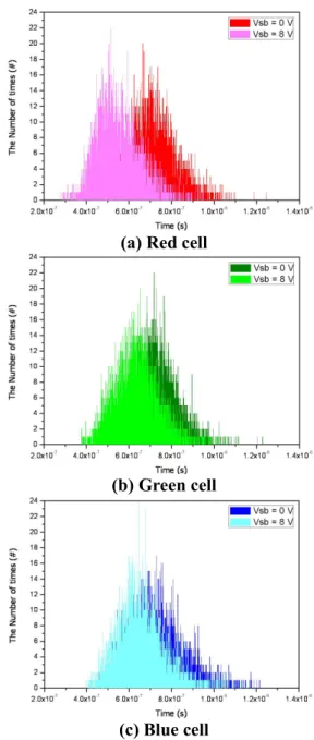
Fig. 4. Black images depending on Vsb. The discharge time lag was measured at Vsb = 0 V
and 8 V. For the measurements, each R, G and B dot pattern at 1 grey level was selected.
(a) Red cell
(b) Green cell
(c) Blue cell
Fig. 5. Distribution of IR emission from address discharge during 5,000 sweep times.
P1-63 / W. H. Park
• IMID 2009 DIGEST
Figure 5 showed the distribution of IR from address discharges at appointed sub-pixel. When Vsb was
applied on scan electrode, distribution of IR emission was shifted to left side and the discharge time lag was reduced.
(a) Red cell
(b) Green cell
(c) Blue cell
Fig. 6. Comparison of Tf depending on Vsb. Figure 6 showed the results of Tf and Tavg depending
on different Vsb. At Vsb = 8 V, the formative (= Tf) and
average discharge time lags (=Tavg) were shorter than
Vsb = 0 V case. In R, G and B sub-pixels, the
formative time lag was reduced about 35.43 %, 33.25 % and 3.16 % respectively.
As shown in Figure 7, the average time lag of each sub-pixel was reduced about 22.96 %, 12.40 % and 9.37 % respectively.
(a) Red cell
(b) Green cell
(c) Blue cell
Fig. 7. Comparison of Tavg depending on Vsb.
4. Summary
The positive scan-bias applied on scan electrode during reset period was improved discharge time lag significantly. Because of the scan-bias voltage, more negative wall-charges were accumulated on scan electrodes were reduced on address electrode. It caused the discharge ignition during address period easily. In each R, G and B sub-pixel, the formative
P1-63 / W. H. Park
IMID 2009 DIGEST • time lag was reduced about 35.43 %, 33.25 % and
3.16 % respectively and the average time lag was reduced about 22.96 %, 12.40 % and 9.37 % respectively.
Our studies can be applied to the Full HD or higher resolution PDPs and the negative waveform can be a good candidate to realize the high speed addressing.
Acknowledgement
This research was supported by a grant (F0004071-2009-32) from Information Display R&D Center, one of the Knowledge Economy Frontier R&D Program funded by the Ministry of Knowledge Economy of Korean government.
5. References
1. T. Komaki, A. Fuse, S. Jinno, M. Kitagawa, and M. Murayama, IDW/AD’05 Digest, pp. 1499-1500 (2005).
2. M. Yoo, E. Hwang, H. Shin, D. Lee, and Y. Cho, SID’05 Digest, pp.1836-1839 (2005).
3. Hyerim Choi, Jungwon Kang, IDW’06, Vol.2, pp.1085-1088 (2006).
4. Sanghoem Eom, Hyunil Park, Sunghak Moon and Jungwon Kang, IDW '07, pp. 843-846 (2007). 5. Cheolhwan Eom, Hyunmuk Lim, Junyoung Lee,
Byounggoo Kong, Hyunil Park, Sunghak Moon, and Jungwon Kang, IMID/IDMC/ASIA DISPLAY '08 Digest, pp.388-391 (2008).
6. C. Eom, H. Lim, J. Lee, H. Park, B. Kong, S. Moon, J. Kang, IDW’08, pp.1957-1960 (2008).