INTRODUCTION
In recent years, the interconnect delay (RC delay) begins to govern the overall device delays in the development of ultra-large scaled integration (ULSI). The interconnect delay can be calculated by Eq. (1) (Bohr 1996; Maier 2001)
4L2 L2
T==RC==2ρεε0
[
mmm++mm]
(1) P2 T2where T is the signal delay time, R the resistance, C the capacitance, ρ the specific resistance of the conductor, ε the dielectric constant of the insulating material, ε0the dielectric constant of vacuum, L the length of the conductor, T the thickness of the conductor, and P the distance between two conducting lines. Therefore, to improve the performance of transistor, people have substituted other lower resistivity metal and lower dielectric constant materials instead of the conventional Al and SiO2, respectively (Shamiryan et al. 2004).
Ion implantation into materials has recently attracted sig-nificant interest due to its role in modification of nano-struc-ture, optical properties and electromagnetic properties (Ki-shimoto et al. 2006; Ogiso et al. 2007). Hydrogen, nitrogen and fluorine are commonly used to modify the thin film materials. Nitrogen ion implantation is a good candidate to amend electrical properties without the structural change (Liu et al. 1997; Saks et al. 2000, 2002; ˙Zukowski et al. 2007; Ma et al. 2008). In this study, the effects of the nitro-gen ion implantations on the SiO2/Si structure were investi-gated.
MATERIALS AND METHODS
The SiO2thin films (200 nm) were deposited on the silicon wafer with (1 0 0) surface orientated p-type single crystal by a RF (13.56 MHz) magnetron sputtering system with a SiO2 target under argon gas plasma. The chamber was evacuated first down to 1.0×10⁻⁶Torr and the depositions were carried out at 10 mTorr argon pressure with a constant power den-sity of 1.233 W cm-2. The thicknesses of these thin films
Journal of Radiation Industry 4 (2) : 143~146 (2010)
─ ─ 143 ──
The Effect of Nitrogen Ion Implantations on Dielectric
Properties of SiO2
Thin Film
Hyun Bin Kim, Joon Pyo Jeun and Phil Hyun Kang*
Advanced Radiation Technology Institute, Korea Atomic Energy Research Institute, Jeongeup 580-185, Korea
Abstract-- The SiO2layers on Si wafers were deposited using a RF-magnetron sputtering system,
and the effects of nitrogen ion implantations on these films were investigated. Nitrogen distribu-tions were observed using an Auger electron spectroscopy, and the dielectric properties were mea-sured using an impedance analyzer. The real part, the imaginary part of permittivity and the ac conductivity of nitrogen ion implanted SiO2layer were changed as increasing the nitrogen ion
implantation. These results were explained based on the nitrogen distribution in the SiO2layer
and the interface of SiO2/Si.
Key words : Nitrogen ion implantation, SiO2, Dielectrics
* Corresponding authors: Phil Hyun Kang, Tel. +82-63-570-3061, Fax. +82-63-570-3068, E-mail. [email protected]
were measured using an alpha-step. Nitrogen ions were im-planted on the SiO2surfaces with 1×10¹⁷, 5×10¹⁷and 1× 10¹⁸N++
ions cm-2at 100 keV. The nitrogen depth profiles
were measured using an AES (Auger electron spectroscopy). To measure the dielectric properties, the Cu electrodes were deposited on the back side of Si wafer with 100 nm using a DC magnetron sputtering system. The upper electrode which has 200 nm thickness and 1.2 cm diameter was deposited on the SiO2layer using a shadow mask. The dielectric properties were investigated using an impedance analyzer (HP 4192A).
RESULTS AND DISCUSSION
1. Depth profile of the nitrogen ions
The depth profiles measured using an AES were shown in Fig. 1. Nitrogen atomic concentrations were slightly increased as increasing the density of nitrogen implantation in the SiO2layer. The nitrogen atomic concentrations were dramatically increased in the SiO2and Si wafer interface. It can be considered that the amorphous SiO2layer has low density as much as accelerated nitrogen ions passing through, and the bonds of silicon and nitrogen atoms are created on the surface of Si wafer. Implanted nitrogen ions were detect-ed till the 100 nm depth from the Si wafer surface. Interface can play a critical role in determining the dielectric propert-ies (Sombra et al. 2002). Interstitial sites of SiO2layer and Si wafer were occupied with nitrogen atoms. It is expected that the electron mobility is reduced by disturbance.
2. Dielectric property variations
The complex permittivity was defined in the following complex form
ε*==ε′-jε′′ (2)
where ε′ and ε′′ are the real and the imaginary of complex permittivity, and j is the imaginary root of -1. This dielect-ric formula is readjusted by many researchers (Tataro˘glu et al. 2007; Dökme et al. 2008). In the ε* formalism, in the case of admittance measurement, the following relation holds:
Y* C G
ε*==mmmm==mm-j mmm (3)
jωC0 C0 ωC0
where Y*, C and G are the measured admittance, capacitance and conductance of the dielectric and ω the angular frequ-ency (ω==2πf) of the applied electric field. The real parts of the dielectric properties were calculated using the following Eq.
ε′==Cm/C0 (4)
C0==ε0(A/d) (5)
ε0is the permittivity of free space charge (ε0==8.85×10⁻¹⁴F cm-1), A is the area of the sample and d is the interfacial in-sulator layer thickness. The frequency dependencies of the real part dielectric constant at room temperature are shown
Hyun Bin Kim, Joon Pyo Jeun and Phil Hyun Kang
144
Fig. 1. Nitrogen ion depth profiles from the SiO2surface to Si wafer measured by an AES.
0 2 4 6 8 10 Log f (HZ) 1 2 3 4 5 6 Control 1.0×10¹⁷N ions cm-2 5.0×10¹⁷ N ions cm-2 1.0×10¹⁸N ions cm-2
Fig. 2. Real part of dielectric constant, versus frequency at different N++ions implantation. A.C. % 0 100 200 300 Depth (nm) 10 8 6 4 2 0 1017N++ions cm-2 5×10¹⁷N++ions cm-2 1018N++ions cm-2 SiO2 Si ε′
in Fig. 2.
The values of real parts at 10 Hz were reduced as increas-ing the nitrogen ion implantation density. It was thought that dipole strength or density of the SiO2layer was reduced by nitrogen ion implantation. The real parts values were dra-matically reduced over 1 kHz and reducing points were shown a shift to high frequency as increasing the ion implan-tation. There results have an intimate relation with imaginary part of permittivity.
The imaginary parts of the complex permittivity are cal-culated using the following relationship:
G
ε′′==mmmm , (6)
ωC0
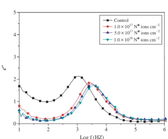
and also shown in Fig. 3. The dielectric properties of all samples have a Debye-like relaxation, i.e., first, the real part of the permittivity displays a step decrease at the frequency where the imaginary part of the permittivity shows a relaxa-tion peak; second, the real part of the permittivity has little frequency dependence below the relaxation frequency (Liu
et al. 2005). Relaxation peak points showed a strong shift
and decrease of amplitude with increasing ion implantations. Reduction in peak amplitude without a change in shape of peak suggested a decrease in total amount of relaxed dipoles. The values of ac electrical conductivity (σac) was shown in Fig. 4 with log frequency, which was calculated from the relation
σac==ωC tan δ (d/A)==ε′′ωε0. (7)
The ac conductivities of ion implanted samples were shown lower values from 10 Hz to 5 kHz. It also shows that the nitrogen atoms in SiO2layer obstruct the electron mobi-lity. However, nitrogen implanted samples show higher conductivity value above the 5 kHz. It was thought that the effects of new bonds in the SiO2/Si interface. The nitrogen atoms are occupied the vacancies in interface. And it help electron jump from Si wafer to SiO2layer. It can be explain the reasons of higher permittivity values were shown in Fig. 2 above the 5 kHz.
CONCLUSION
In this study, we investigated the effects of the nitrogen ions implantations on the MOS which has SiO2/Si structure. The real parts of permittivity were decreased in low frequ-ency and the peaks in the imaginary parts showed shift to higher frequency. Theses results can be explained by effects of nitrogen atoms in SiO2layer and in the SiO2/Si interface. Therefore, we are convinced that the nitrogen ion implanta-tion has great potential for new applicaimplanta-tion in development in low dielectric materials.
ACKNOWLEDGMENT
This research was supported by the Nuclear R&D program through the Korea Science and Engineering Foundation
Nitrogen Ion Implantation on SiO2Thin Film 145
0 1 2 3 4 5 Log f (HZ) 1 2 3 4 5 6 Control 1.0×10¹⁷ N ions cm-2 5.0×10¹⁷N ions cm-2 1.0×10¹⁸ N ions cm-2
Fig. 3. Imaginary part of dielectric constant, versus frequency at
different N++ions implantation.
Log f (HZ) 1 2 3 4 5 6 10-3 10-4 10-5 10-6 10-7 10-8 10-9 10-10 σac (Ω -1 cm -1) Control 1.0×10¹⁷N ions cm-2 5.0×10¹⁷ N ions cm-2 1.0×10¹⁸N ions cm-2 ε′′
Fig. 4. AC conductivity (σac), versus frequency at different N++ions
funded by the Ministry of Education, Science and Techno-logy, Korea.
REFERENCES
Bohr MT. 1996. Interconnect scaling-The real limiter to high performance ULSI. Solid State Technol. 39(9):105-111. Dökme , Alt ndal S¸ and Gökçen M. 2008. Frequency and gate
voltage effects on the dielectric properties of Au/SiO2/n-Si structures. Microelectronic Engineering 85:1910-1914. Kishimoto N, Plaksin OA, Masuo K, Okubo N, Umeda N and
Takeda Y. 2006. Electronic excitation effects on nanoparti-cle formation in insulators under heavy-ion implantation. Nucl. Instr. and Meth. B. 242:186-189.
Liu CT, Ma Y, Becerro J, Nakahara S, Eaglesham DJ and Hil-lenius SJ. 1997. Light nitrogen implant for preparing thin-gate oxides. IEEE Electron Device Letters 18:105-107. Liu J, Duan C, Mei WN, Smith RW and Hardy JR. 2005.
Di-electric properties and Maxwell-Wagner relaxation of com-pounds ACu3Ti4O12(A==Ca, Bi2/3, Y2/3, La2/3). Journal of
Applied Physics 98(093703):1-5.
Ma M, Chen C, Su C, Wu W, Yang T, Kao K, Chao T and Lei T. 2008. Improvement on performance and reliability of TaN/HfO2LTPS-TFTs with fluorine implantation.
Solid-State Electronics 52:342-347.
Maier G. 2001. Low dielectric constant polymers for
microelec-tronics. Prog. Polym. Sci. 26:3-65.
Ogiso H, Nakada M, Nakano S and Akedo H. 2007. THz spec-troscopy of ion-implanted MgO crystals. Nucl. Instr. and Meth. B. 257:545-548.
Saks NS, Agarwal AK, Mani SS and Hegde VS. 2000. Low-dose nitrogen implants in 6H-silicon carbide. Applied Phy-sics Letters 76:1896-1898.
Saks NS, Ryu SH and Suvorov AV. 2002. Low-dose n-type nitrogen implants in 4H-SiC. Applied Physics Letters 81: 4958-4960.
Shamiryan D, Abell T, Iacopi F and Maex K. 2004. Low-k dielectric materials. Materialstoday Jan.:34-39.
Sombra SS, Costa UMS, Freire VN, de Vasconcelos EA and da Silva EF Jr. 2002. The role of multiple damaged layers at the Si/SiO2interface on the dielectric breakdown of MOS capacitors. Applied Surface Science 190:35-38.
Tataro˘glu A, Alt ndal S¸ , Bölükdemir MH and Tan r G. 2007. Irradiation effect on dielectric properties and electrical con-ductivity of Au/SiO2/n-Si (MOS) structures. Nucl. Instr.
and Meth. in Phys. Res. B. 264:73-78.
˙Zukowski P, Ko tunowicz T, Partyka J, W gierek P, Koma-rov FF, Mironov AM, Butkievith N and Freik D. 2007. Dielectric properties ad model of hopping conductivity of GaAs irradiated by H++ions. Vacuum 81:1137-1140.
Manuscript Received: May 24, 2010 Revision Accepted: June 7, 2010 l
Hyun Bin Kim, Joon Pyo Jeun and Phil Hyun Kang 146