P1-66 / C.-H. Moon
• IMID 2009 DIGEST
New Electrode Designs for High Luminous Efficiency in AC PDP
Cheol-Hee Moon, Jae-Seung Moon
Dept. of Display Engineering, Hoseo University, Asan city,
Chungnam, 336-195 Korea
Phone: 041-540-5923, E-mail: [email protected]
Abstract
In this paper we proposed a new electrode design to get an enhanced luminous efficiency in AC PDP. The width and shape of the TTO electrode were varied, and the electro-optical properties such as luminance, power consumption, luminous efficiency were estimated with the variation of frequency, duty ratio and applied voltage. The discharge characteristics were investigated to explain the effect of the new electrode structure on the electro-optical properties.
1. Objectives and Background
Recently, a decrease in the power consumption of the PDP TV has become one of the most important issues in the development of PDP TVs. High luminous efficacy technologies are needed to decrease the power consumption in AC PDP. As for the present PDP, white luminous efficacy is about 2 lm/W.
There have been many kinds of approaches to increase the luminous efficiency of PDP. The first approach is to use higher Xe content discharge gas. The higher increment of luminous efficiency with higher Xe content discharge gas in various cell designs of AC PDP is well known. Mechanism of the high luminous efficient discharge[1], electric field and priming particle effect[2] and the effect of the driving pulse[3] have been reported for high Xe content AC PDP.
Second approach to get a high luminous efficiency is to change the electrode structure such as ITO electrode and bus electrode. The change of the electrode structure includes the width, shape, position and material etc. It also has been reported that the driving conditions such as driving voltage, frequency and duty ratio can affect the luminous characteristics of PDP. Currently, T. Akiyama etc. reported that they could get a luminous efficacy of around 5 lm/W by using a high-Xe-content gas
mixture. [4],[5],[6] J. P. Boeuf etc. reported on the large-gap AC coplanar structure[7]. The effect of the bus electrode position on the ITO electrode line[8], change of the ITO electrode[9], discharge characteristics with respect to width of address electrode[10] etc. have been reported also.
Our laboratory has reported on the new concept electrode structure, IBS (ITO-bus separated) structure to get an enhanced luminous efficiency. The mechanism of the higher luminous efficiency in the IBS electrode structure[11], the effect of the number of the auxiliary electrode[12] and the change of the bright room contrast ratio with respect to the width of the electrode[13] have been reported on the IBS electrode structure.
In this paper, using IBS electrode structure in Fig.1, the effects of some design factors on the luminous efficacy of PDP were investigated. Luminous characteristics and some electrical characteristics were estimated and analyzed with the discharge characteristics.
2. Experimental
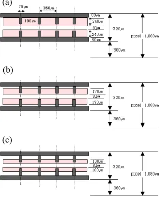
The 3-inch test panels have been manufactured with a cell size of 360 ㎛ by 1,080 ㎛ following the general specification of 42-inch SD(standard definition) PDP. ITO coated 2.8mm-thick PD200 glass substrates were used for the front substrates.
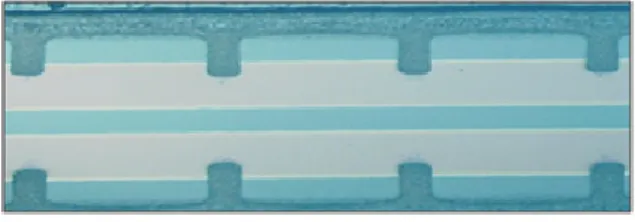
Fig. 1. Microscope image of the IBS electrode structure which was studied in this paper.
P1-66 / C.-H. Moon
IMID 2009 DIGEST • ITO electrode patterns and bus electrode patterns
were manufactured by photolithography. To decrease the experimental errors, conventional electrode pattern and IBS electrode pattern were placed together in a same panel. We varied the widths of the ITO electrodes as 240, 170 and 100 ㎛ as is shown in Fig.2. 30 ㎛ thick-transparent dielectric layer was formed on the ITO and BUS electrode, and 6000Å-thick MgO layer was coated on it by electron beam evaporation method. Barrier ribs were manufactured by chemical etching method, and green phosphors were printed into the cell volumes. Front and rear substrates were assembled by sealing frits and inner cell volumes were filled with Ne-Xe 5%(400Torr) gas mixture after exhausted at 350 .℃
3. Results
The discharge and luminous characteristics of the panel were measured with the application of 25 kHz of sustained pulses with a 25% duty ratio. All the characteristics of the panel were observed at the median of the measured voltage margin. The luminance (cd/㎡) was measured with a luminance calorimeter (BM-7, TOPCON), and the electrical
power consumption (W) was calculated using the following equation:
off on P P
P= − Eq. 1 wherein Pon and Poff are the power consumptions
when all the cells are on and off, respectively. The luminous efficiency was estimated using the following equation: P S L
π
η
= Eq. 2 wherein L is the luminance, S is the total area of the discharge cells, and P is the power consumption. The evolution of the emission lights within a discharge cell was observed using ICCD (C8484-05G, Hamamatsu), and 200 V of sustained pulses were applied at a frequency of 35 kHz and a 25% duty ratio.Fig. 3 shows the comparison of the luminous efficacy data for the different ITO widths. It is shown that the luminous efficacy increases with the decrease of the ITO width, and about 2 lumen/watt was obtained for the ITO width of 100 ㎛, about 30% higher than that of 240 ㎛ in Fig. 3.
Fig. 2. Schematic drawing of the electrode design studied in this paper.
(a)
(b)
(c)
Fig. 3. Luminous efficacy for the electrode structures with different ITO width.
P1-66 / C.-H. Moon
• IMID 2009 DIGEST
Fig. 4 shows the comparison of the luminance data for the different ITO widths. It is shown that the luminance decreases with the decrease of the ITO width, and the luminance data for the ITO width of 100 ㎛ shows about 30% lower than that of 240 ㎛ in Fig. 4.
This means that the narrower ITO width (100 ㎛) shows higher luminous efficacy, but it doesn’t gives higher luminance. That is, the enhancement of the luminous efficacy of the 100 ㎛ -ITO width is not due to the higher luminance but due to the smaller power consumption in Eq. 2. This is not promising if considering the luminance only, because more electrical power has to be supplied and additional electrical parts have to be required to meet the customers’ requirement for luminance of the PDP TV.
However, narrower ITO structure provides the opportunity of getting higher blackness of the panel giving more area for the black stripe to be placed.
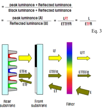
As is shown in Eq. 3, the bright room contrast ratio is the relative value of the peak luminance and the reflected luminance. Using the narrow ITO structure (and broader black stripe), the reflected luminance can be reduced, which gives higher value of the bright room contrast ratio in Eq. 3. In this case, therefore, we can use higher transmittance optical filter, which means higher luminance can be obtained in the PDP TV set.
Conclusively, the narrower ITO structure in this paper is helpful to get higher luminous efficacy, and
the drawback, lower luminance, can be recovered adopting the higher contrast ratio structure.
Eq. 3
4. Summary
We have found that the narrower ITO electrode in IBS structure can give a higher luminous efficiency. This is also promising in the sense that in this structure blackness of the PDP panel can be enhanced, which gives a higher value of the bright room contrast ratio.
5. Acknowledgement
This work was supported by the IT R&D program of MKE/KEIT. (2009-S-009-01, Development of Eco-friendly 50” Quadro Full HD PDP Technology)
6. References
[1] W. J. Chung, B. J. Shin, T. J. Kim, H. S. Bae, J. H. Seo and K. W. Whang, IEEE Trans. on
Plasma Science, 31/5, pp.1038-1043(2003)
[2] J. S. Kim, J. H. Yang, T. J. Kim and K. W. Whang, IEEE Trans. on Plasma Science, 31/5, Fig. 4. Luminance for the electrode
structures with different ITO width.
Fig. 5. Several factors which determine the bright room contrast ratio in PDP TV sets.
P1-66 / C.-H. Moon
IMID 2009 DIGEST • pp.1083-1090(2003)
[3] K. C. Choi and H. J. Cho, IEEE Trans. on
Consumer Electronics, 49/2, pp.253-256(2003)
[4] T. Akiyama, T. Yamada, K. Shinoda and M. Kitagawa, Journal of the SID, 16/8, pp835-845 (2008).
[5] T. Akiyama, T. Yamada, M. Kitagawa and T. Shinoda, SID Symposium Digest, pp378-381(2008).
[6] T. Akiyama, T. Yamada and M. Kitagawa,
Journal of the SID, 17/2, pp121-130(2009).
[7] J. Ouyang, Th. Callegari, B. Caillier and J. P. Boeuf, IEEE Trans. on Plasma Science, 31/3, pp.422-428(2003)
[8] J. Kang, IEEE Trans. on Plasma Science, 34/2, pp.371-375(2006)
[9] C. H. Park, S. H. Lee, D. H. Kim, Y. K. Kim and J. H. Shin, IEEE Trans. on Electron Devices, 48/10, pp.2255-2259(2001)
[10] H. S. Jeong, Yukio Murakami, Masahiko Seki and Hiroshi Murakami, IEEE Trans. on Plasma
Science, 29/3, pp.559-565(2001)
[11] C. H. Moon and K. N. Kim, Jap. J. of Applied
Physics, 47/4, pp.2259-2261(2008)
[12] C. H. Moon, J. of Information Display, 9/1, pp.20-25(2008)
[13] K. N. Kim, S. H. Yang and C. H. Moon,