45-2 / H. -W. Cheng
• IMID 2009 DIGEST
Abstract
TFT-LCD display system is nowadays one of power-hungry components in portable products; technique of power reduction is thus essential for production of mobile phone. In this work, we minimize the display power, using computationally intelligent statistical methodology. Compared with a conventional design, 68.474% reductions on the current consumption could be obtained for a 2.2-inch of TFT-LCD display system of mobile phone. The total power consumption of the display system consisting of the backlight system and current consumption of display panel is thus successfully reduced form 68.305mW to 64.06mW (about 6.215% reductions).
1. Introduction
Power consumption has become the critical issue for designing the mobile phone. One of the most power-hungry components in the mobile phone is the display system [1-3]. Thus, power minimization of display system is essential for achieving high performance mobile phone. For a display system, the major power dissipation is resulted from the backlight system [2], the driver ICs [3], and the TFT-LCD panel. Display design is technologically complicated and time-consuming task because it requires the full three-dimensional (3D) technology computer-aided design (TCAD) and circuit simulation for all pixels.
2. The Method and Results Discussion
Applying the design of experiment (DOE) [4], the
response surface model (RSM) [5,6], and CAD simulation tools, proper statistical models with respect to interested electrical and optical characteristics are formulated in terms of various design parameters, such as the size variation of pixel, the driving conditions, etc. Consequently, we minimize total power consumption including power dissipation of TFT-LCD panel and backlight part for 2.2”-2.6” display system of mobile phones using a genetic algorithm. The preliminary results of this study elucidate a systematical parameterization technique for display system design automation.
Table 1 lists the upper and lower bounds of interested designing parameters for designing a 2.2” display system of mobile phones, where parameter A is the panel size of the display system, parameters B to G are related to capacitances of the TFT-LCD pixel in pixel level design, and parameter H is the gate voltage for driving circuits in panel level. Power dissipation of a display system could be resulted from rather different factors; among them, we consider two main factors, the power consumption of the backlight system and TFT-LCD panel, for designing a display system of mobile phone with minimal power consumption. For the power consumption of backlight system, we reduce the power dissipation by increasing the aperture ratio of the display panel for achieving the same brightness of the display system. For the power consumption of TFT-LCD panel, we suppress the current consumption of the scan line and data line.
Table 2 lists comparison result between a conventional design and our approach of the tested
An Optimal Design for Power Consumption of 2.2”~2.6”
Display System of Mobile Phone
Hui-Wen Cheng
1, Hsuan-Ming Huang
1, Yiming Li
1,2,3,*, Tseng-Chien Tsai
4,
Hung-Yu Chen
4, Kuen-Yu Huang
4, and Tsau-Hua Hsieh
41Institute of Communication Engineering, National Chiao-Tung University, Hsinchu 300, Taiwan 2Department of Electrical Engineering, National Chiao-Tung University, Hsinchu 300, Taiwan
3National Nano Device Laboratories, Hsinchu 300, Taiwan
4LCD Platform Technology Division, InnoLux Display Corporation, Science-Based Industrial Park, Chu-Nan 350, Miao-Li County, Taiwan
*Tel: 886-3-5712121 ext. 52974, e-mail: [email protected]
45-2 / H. -W. Cheng
IMID 2009 DIGEST •
TABLE 1. List of the upper and lower bounds of the designing parameters in the examined case.
Variable Parameters Variation range Panel layout sizing (inch)
A Panel layout sizing [2.2, 2.6] Pixel layout variation (µm)
B Gate line and common
line spacing [5, 10] in y C Gate line and ITO
electrode spacing [1.5, 4.5] in y D Data line width [3.5, 5] in y E Shielding metal and ITO
electrode overlap width [2, 3] in x F Data line and left
shielding metal spacing [1.5, 3.5] in x G Data line and right
shielding metal spacing [1.5, 3.5] in x Driving setting
H Gate voltage (V) [20, 30]
TABLE 2. Comparison between a conventional design and our result for the tested case.
Design
Performances
Spec.
Conventional
Procedure Our Approach
Result Behavior Model SimulationCAD Error (%) Crosstalk area (%) < 1.2% 0.85 0.9012 0.9001 0.12 Crosstalk vertical (mV) < 10mV 1.00146 1.192 1.14213 4.18 Flicker (dB) < -30dB -40.3194 -35.36 -32.8412 7.12 Current consumption of display panel (mA) < 0.7mA 0.698517 0.215208 0.21801 0.13 Aperture ratio (%) > 50% 49.031 51.094 51.13 0.07 Current consumption of backlight module (mA) < 21mA 20 19.188 19.1744 0.07
2.2” display panel of mobile phone. Compared with the conventional design, we have successfully reduced the power consumption from 68.305mW to 64.06mW (about 6.215% reductions), where an increment of the aperture ratio is from 49.031% to 50.8768% and the reduction of the current consumption of TFT-LCD panel is about 68.474% (from 0.698mA to 0.22mA), using the CAD simulation validated statistical models. The statistical models estimate a similar power consumption of the display system, compared with the data of the CAD simulation. The error of power consumption of the whole display system between the
(a)
(b)
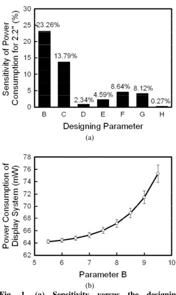
Fig. 1. (a) Sensitivity versus the designing parameters of the power consumption of whole display system. (b) The power consumption of whole display system versus the variation of the parameter B.
behavioral models and CAD simulations is within 1%. In additional, critical concerns of the display performances, such as the crosstalk and the flicker are also similar to CAD simulations, as shown in Tab. 2.
After the optimization design, the qualitative and sensitivity analysis are then performed. Figure 1(a) shows the sensitivity of the 2.2” display panel of mobile phone, where the spacing between the gate line and common line (i.e., the parameter B) is the dominating factor in the power consumption of whole display system. The spacing between the gate line and common line directly effects the aperture ratio of the display panel and the power dissipation of the backlight module of the mobile phone. Figure 1(b) shows the power consumption versus the parameter B,
45-2 / H. -W. Cheng
• IMID 2009 DIGEST (a)
(b)
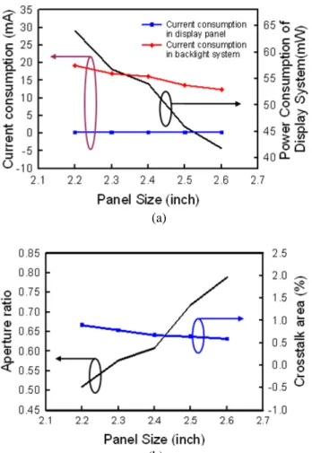
Fig. 2. (a) Dependence of the power consumption of the display system on the panel size varying from 2.2” to 2.6”. (b) Plot of the aperture ratio and the crosstalk area of the optimal display panel from 2.2” to 2.6”.
where the error bar indicates the variation of the power consumption with respect to different B. The variation of each B is assumed to be a Gaussian distribution (which is with more than 10,000 trails and 3σ, practically determined by the practical process variation, is about 0.25 µm). We note that the other parameters are constant when the examination of Fig. 1(b) is performed. As the spacing between the gate line and the common line varying from 5.5 µm to 9.5 µm, the variation of power consumption (σP) is increased by 1.1083 mW. The increase of σP mainly results from the relatively sensitive of the power consumption with respect to the space variation, and thus induces significant variance of the power consumption.
Figure 2(a) shows the achieved design for the power consumption of the display panel from 2.2” to 2.6”. The red and blue lines are the current dissipation of backlight system and TFT-LCD panel, respectively. As the display panel size increases, the current dissipation of TFT-LCD panel are increased slightly. However, the current dissipation of backlight system
TABLE 3. The upper and lower bounds of the designing parameters in the 17” TFT-LCD panel.
Variable Parameters Variation range Layout size variation (µm)
A Gate line [0,7] in y
B Shielding metal (left) [0,3] in x C Shielding metal (right) [0,3] in x
D Data line [0,3] in x
E ITO electrode left side [0,5] in x F ITO electrode right side [0,5] in x G ITO electrode top side [0,5] in y
Driving setting
H Gate voltage (V) [20,30]
I Hold time of gate (µs) [8,16]
J Cutting voltage (V) [12,20] K Cutting time (µs) [1,3]
decreases significantly which dominates the power dissipation of the whole display system. The reduction of the current dissipation is owing to the same resolution of the display panel. The aperture ratio will increase since the panel become lager as shown in Fig. 2(b). Therefore, the power dissipation of the backlight system will be reduced by increment of aperture ratio of the optimal display panel. Moreover, Fig. 2(b) also indicates the optimal designs were done well to achieve the other critical designing specifications.
The current consumption is also one of the most significantly limiting factors for the large-screen-size and high-resolution TFT-LCD design. Therefore, the current consumption of a 17” TFT-LCD panel is further studied. The designing parameters of the 17” TFT-LCD panel are listed in Tab. 3. The current consumption of the gate line and the data line are considered to reduce the current consumption of the TFT-LCD panel. We reduce the current consumption of the TFT-LCD panel from 69.12 mA to 58.42 mA, as shown in Tab. 4. The current consumption of the gate line is increase from 0.54 mA to 0.64 mA, but the current consumption of data line which dominates the total current consumption of the TFT-LCD panel is reduced from 68.58 mA to 57.78 mA.
45-2 / H. -W. Cheng
IMID 2009 DIGEST •
TABLE 4. Optimal design of the investigated 17” TFT-LCD panel.
Performances Spec Original Optimal Crosstalk (area) < 1.2 % 0.07 0.9 Crosstalk (vertical) < 10 mV 4.52 1.31e-5 Gate delay (us) < 10 µs 3.31 4.35
Igateline (mA) 0.54 0.64
Idataline (mA) 68.58 57.78
Charging capability (C) > 3.5 RC 7.27 36.38 Charging capability (E) > 3.5 RC 6.14 24.34 Vcom (center) (mV) < 100 mV 37.35 0.97 Vcom (left) (mV) < 100 mV 33.75 19.55 Vcom (right) (mV) < 100 mV 3.6 21.78 Time for 90% CR (C) < 10 µs 6.27 2.89 Time for 90% CR (E) < 10 µs 8.05 2.85
Mura 0.02 0.02
(a)
(b)
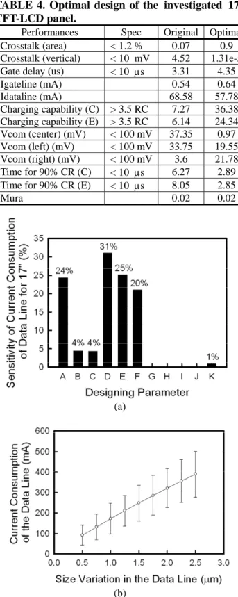
Fig. 3. (a) Sensitivity of the current consumption of the data line of the examined case versus each parameter. (b) The current consumption versus the size variation in the data line.
The sensitivity of the current consumption of the data line with respect to each parameter is shown in
Fig. 3(a). There is 53 mA increase of the standard deviation of the current consumption of the data line 5 when data line varies from 0.5 µm to 2.5 µm, as shown in Fig. 3(b). The increase of fluctuation of the current consumption of the data line is mainly due to relatively large variations of the performance when the variance of the data line increase. This estimation could be examined by individually constructing RSMs with respect to TFT-LCD panel.
3. Summary
In this work, we have successfully studied the power consumption of 2.2”-2.6” TFT-LCD display panel for mobile phones. Compared with a conventional design, our approach for a 2.2” case increases the aperture ratio of the panel from 49.031% to 50.8768% and reduces the current consumption of TFT-LCD panel from 0.698 mA to 0.22 mA (68.474% reductions), and the reduction of total power dissipation is 6.215%. Similarly, we also reduced the current consumption of a 17” TFT-LCD panel from 69.12 mA to 58.42 mA. This approach can be incorporated into simulation flow for TFT-LCD design and may benefit the design automation of display panels.
Acknowledgement
This work was supported in part by National Science Council (NSC), Taiwan under Contract NSC-97-2221-E-009-154-MY2 and by the Innolux Display Corp., Chu-Nan, Taiwan under a 2006-2008 grant.
4. References
1. C. T. Liu, J. of Display Technology, 3, pp. 342-350 (2007).
2. N. Chang, I. Choi, H. Shim, IEEE Trans. VLSI
Systems, 3, pp. 827-846 (2004).
3. S. Y. Park, S. H. Son, and W. S. Chung, IEEE
Trans. Consumer Electronics, 4, pp. 1589-1594
(2007).
4. Y. Li, Y.-L. Li, and S.-M. Yu, Math. Comput.
Simulation, 79, pp. 1165-1177 (2008).
5. R. H. Myers and D. C. Montgomery, Response
Surface Methodology: Process and Product Optimization Using Designed Experiments, John
Wiley Sons Inc., 2002.
6. C. F. Cheng, S. Jagar, M. C. Poon, C. W. Kok, and M. Chan, IEEE Trans. Elec. Devices, 51, pp. 2061–2068 (2004).