저작자표시-비영리-동일조건변경허락 2.0 대한민국 이용자는 아래의 조건을 따르는 경우에 한하여 자유롭게
l 이 저작물을 복제, 배포, 전송, 전시, 공연 및 방송할 수 있습니다. l 이차적 저작물을 작성할 수 있습니다.
다음과 같은 조건을 따라야 합니다:
l 귀하는, 이 저작물의 재이용이나 배포의 경우, 이 저작물에 적용된 이용허락조건 을 명확하게 나타내어야 합니다.
l 저작권자로부터 별도의 허가를 받으면 이러한 조건들은 적용되지 않습니다.
저작권법에 따른 이용자의 권리는 위의 내용에 의하여 영향을 받지 않습니다. 이것은 이용허락규약(Legal Code)을 이해하기 쉽게 요약한 것입니다.
Disclaimer
저작자표시. 귀하는 원저작자를 표시하여야 합니다.
비영리. 귀하는 이 저작물을 영리 목적으로 이용할 수 없습니다.
동일조건변경허락. 귀하가 이 저작물을 개작, 변형 또는 가공했을 경우 에는, 이 저작물과 동일한 이용허락조건하에서만 배포할 수 있습니다.
공학박사 학위논문
Orange and White Organic Light- Emitting Diodes using Exciplex-
forming Co-hosts
엑시플렉스를 이용한 황색 및 백색 유기발광다이오드 연구
2014년 2월
서울대학교 대학원
재료공학부 하이브리드재료 전공
이 성 훈
i
Abstract
Orange and White Organic Light- Emitting Diodes using Exciplex-forming
Co-hosts
Sunghun Lee Department of Materials Science and Engineering The Graduate School Seoul National University
White organic light emitting diodes (WOLEDs) have great potential for applications in displays, lighting, automobiles, imaging, and medicine. In this thesis, various approaches to develop highly efficient WOLEDs using exciplex forming co-hosts are studied in detail.
This thesis consists of four parts; (1) orange OLEDs (chapter 2~4), (2) multi-EML WOLEDs (chapter 5), (3) a mechanism of charge generation units (CGUs) and an efficient CGU, and (4) Tandem WOLEDs. All OLEDs use exciplex forming co-hosts to achieve high efficiency, low driving voltage, and low efficiency roll-off, simultaneously.
Chapter 1 summarizes the operating principle of OLEDs and what is the exciplex and how to incorporate the exciplex into OLEDs. Various layouts for WOLEDs are introduced and the quality of WOLEDs for lightings is briefly discussed in terms of the efficiency and color quality.
Chapter 2~4 introduce orange OLEDs which are the key building block for development of efficient WOLEDs with high color rendering index (CRI). In chapter 2, an exciplex forming co-host is introduced in order to fabricate orange OLEDs with high efficiency, low driving voltage and an extremely low efficiency roll-off, by the co-doping of green and red
ii
emitting phosphorescence dyes in the host. The orange OLEDs achieved a low turn-on voltage of 2.4 V, which is equivalent to the triplet energy gap of the phosphorescent-green emitting dopant, and a very high external quantum efficiency (EQE) of 25.0%. Moreover, the OLEDs showed low efficiency roll-off with an EQE of over 21% at 10,000 cdm-2. The device displayed a very good orange color (CIE of (0.501, 0.478) at 1,000 cdm-2) with very little color shift with increasing luminance. The color shift is supposed to be originated from a light doping concentration of red dopants. The transient electroluminescence (EL) of the OLEDs indicated that both energy transfer (ET) and direct charge trapping took place in the devices. In chapter 3, the recombination mechanism of red emission in orange OLEDs with co-doping of green and red phosphorescent dopants is studied using transient EL analysis in decay region. The dominant recombination type is the ET from green to red dopants and the efficiencies of ET were calculated about 50% in various orange OLEDs using decay rate constants of green emission without red dopant and ET rate constants from green to red dopants. In addition, we showed the energy of transition dipole with the same orientation is more efficiently transferred to that of the same orientation, because the ET is a function of transition dipole orientation. Furthermore, we demonstrated an unprecedentedly efficient orange OLED exhibiting the maximum EQE of 32.2% using green and red dopants having horizontally oriented transition dipole moments. In chapter 4, a high performance orange OLED where red and green phosphorescent dyes are doped in an exciplex forming co-host as separate red and green emitting layers (EMLs). The OLED shows a maximum EQE of 22.8%, a low roll-off of efficiency with an EQE of 19.6% at 10,000 cd/m2, and good orange color with a CIE coordinate of (0.442, 0.529) and no color change from 1,000 to 10,000 cd/m2.
In chapter 5, a novel structure for highly efficient WOLEDs approaching the theoretical limit is studied by combining exciplex forming co-hosts, horizontally oriented
iii
phosphorescence dyes, and two emission layers for three colour white emission. The WOLED showed a maximum luminous efficacy (LE) of 68 lm W–1 and maximum EQE of 28.8% without an extra light extraction layer. Furthermore, the device exhibited high LE at high luminance with a LE of 58 lm W–1 at 1,000 cd m–2 originating from a high EQE (27.9%), low operating voltage (3.52 V) and low efficiency roll-off. The device emitted high quality warm white light with a CRI of 82. In addition, we achieved a LE of 106 lm W–1 at 1,000 cd m–2 by attaching an index-matched glass half sphere to the glass substrate.
In chapter 6, the rate limiting step of charge generation is studed using the CGUs composed of a p-doped hole transporting layer (p-HTL), 1,4,5,8,9,11-hexaazatriphenylene hexacarbonitrile (HATCN) and n-doped electron transporting layer (n-ETL) where 1,1-bis- (4-bis(4-methyl-phenyl)-amino-phenyl)-cyclohexane (TAPC) was used as the HTL.
Energy level alignment determined by the capacitance-voltage (C-V) measurements and the current density-voltage characteristics of the structure clearly showed that the electron injection at the HATCN/n-ETL junction limits the charge generation in the CGUs rather than charge generation itself at the p-HTL/HATCN junction. Consequently, the CGUs with 30 mol% Rb2CO3 doped BPhen formed with the HATCN layer generates charges very efficiently and the excess voltage required to generate the current density of ±10 mA/cm2 was around 0.17 V, which is extremely small compared with the literature values reported up to now.
In chapter 7, tandem WOLEDs with EQE approaching theoretical limit are reported by interconnecting high efficiency orange OLEDs with co-doping of green and red phosphorescent dopants having high Θ andφPL in exciplex forming co-host (concept shown in chapter 2, 3) and blue OLED using exciplex forming co-host with an efficient CGU (shown in chapter 6). A tandem WOLED with a high maximum EQE of 54.3% (PE of 63 lm W–1), EQE of 52.6% (PE of 52 lm W–1) at 1,000 cd m–2, low efficiency roll-off, and high
iv
color stability was demonstrated. In addition, an EQE of 90.6% at 1,000 cd m–2 by attaching an index-matched glass half sphere on conventional glass substrate was achieved.
Keywords: exciplex-forming co-host, organic light-emitting diodes, orange OLEDs, white OLEDs, charge generation units, tandem OLEDs
Student Number: 2010-30782
v
Contents
Abstract ... i
List of Tables... ix
List of Figures... x
Chapter 1. Introduction ... 1
1.1 Organic light emitting diodes ... 1
1.2 Operating principles of organic light-emitting diodes... 5
1.1.1 Basic device configurations and functional layers ... 5
1.1.2 Intermolecular energy transfers ... 7
1.1.3 Charge balance factor and prediction of efficiency in organic light emitting diodes ... 10
1.3 Exciplex-forming co-hosts for organic light-emitting diodes with ultimate efficiency... 14
1.4 White organic light-emitting diodes... 19
1.5 Outline of thesis ... 24
Chapter 2. Orange Organic Light Emitting Diodes with Controlled Co- doping of Green and Red Phosphorescent Dopants in an Exciplex forming Co-host ... 26
2.1 Introduction ... 26
2.2 Experimental ... 28
2.3 Result and Discussion ... 30
2.4 Conclusion ... 42
Chapter 3. Orange Organic Light-Emitting Diodes with Co-Doping of Green
vi
and Red Dopants: Energy Transfer and Orientation Effect in Co-
Dopants ... 43
3.1 Introduction ... 43
3.2 Experimental ... 44
3.3 Result and Discussion ... 46
3.4 Conclusion ... 58
Chapter 4. Non-Color-Changing Orange Organic Light Emitting Diodes with Red and Green Emitting Layers ... 59
4.1 Introduction ... 59
4.2 Experimental ... 61
4.3 Result and Discussion ... 62
4.4 Conclusion ... 71
Chapter 5. High quality white organic light-emitting diodes with power efficacy over 100 lm W
–1... 72
5.1 Introduction ... 72
5.2 Experimental ... 73
5.3 Result and Discussion ... 75
5.4 Conclusion ... 88
Chapter 6. The Mechanism of Charge Generation in Charge Generation Units composed of p-doped hole transporting layer/HATCN/n- doped electron transporting layers ... 89
6.1 Introduction ... 89
vii
6.2 Experimental ... 90
6.3 Result and Discussion ... 91
6.4 Conclusion ... 103
Chapter 7. High Efficiency Orange and Tandem White Organic Light- emitting Diodes with External Quantum Efficiency Approaching Theoretical Limit ... 106
7.1 Introduction ... 106
7.2 Experimental ... 107
7.3 Result and Discussion ... 108
7.4 Conclusion ... 122
References ... 124
viii
Abstract in Korean ... 134
Curriculum Vitae ... 138
List of Awards ... 140
List of Publications ... 141
List of Presentations ... 144
List of Patents ... 149
Acknowledgement ... 156
ix
List of Tables
Table 2.1 The details of the performances of the OLEDs ... 35 Table 3.1 The summary of rate constants, lifetimes, and energy transfer
efficiencies ... 56 Table 3.2 Experimentally measured maximum EQEs and calculated EQEs
of orange OLEDs using classical dipole model with assumption of perfect charge balance in the devices ... 57 Table 4.1 Summary of the performance of the Orange OLEDs ... 66 Table 5.1 Performance of WOLEDs with different red dye doping
concentration at luminance of 1,000 cd m
–2, except for maximum LE and EQE. ... 83 Table 6.1 Energy levels of the electronic structure and electron motilities of
HATCN, BPhen, B3PYMPM and TPBi ... 93 Table 6.2 The determined interface energy alignment properties and device
characteristics of CGU devices with BPhen, B3PYMPM and TPBi ... 101 Table 7.1 The details of the performances of the orange and tandem white
OLEDs at luminance of 1000 cd m
-2,except for maximum PE and
EQE ... 121
x
List of Figures
Figure 1.1 (a) Curved television (LG Display 2013). (b) Curved smart phone (Samsung Display 2013). (c) Transparent OLED display (Samsung Display 2011). (d) OLED flexible lighting (LG chem.
2013) ... 4
Figure 1.2 (a) The basic architecture of a typical bottom emitting OLED. (b) The schematic physical processes in a multi-layered OLED. . 6
Figure 1.3 The schematic diagrams for (a) Förster energy transfer and (b) Dexter energy transfer. ... 9
Figure 1.4 (a) The schematic device structure with hole current (J
h), electron current (J
e), leakage current (J
e’ and Jh’), recombination current (J
r), and total current (J). (b) The schematic illustration of charge balance factors with various situations of electron, hole, and recombination currents. ... 11
Figure 1.5 Contour plot of the simulation results of EQE as a function of q
PLand Θ . The two dashed lines indicate the locus of the EQE for Θ
= 0.77 and q
PL = 0.94, respectively. In a similar manner, the dotted lines indicate the EQE for Θ = 0.67 (isotropic), 0.75,and 0.79,
respectively.
22... 13
xi
Figure 1.6 Excitons with different fadii: diagram of (a) a Frenkel exciton, (b) a Wannier exciton, and (c) a charge-transfer (CT) exciton.
2315
Figure 1.7 Potential energy diagram correlating the spectral region of the emission band I(λ) with the intermolecular distance.
24... 16
Figure 1.8 The schematic device structure with energy diagram using an exciplex-forming co-host composed of a hole transporting material (HTM) and an electron transporting material (ETM) as well as the HTM and ETM are used for a HTL and an ETL18
Figure 1.9 The various device layouts to realize high quality white color emission. (a) Single EML doped with red, green, and blue phosphorescent dyes. (b) Side-by-side structures with red, green, and, blue pixels. (c) Side-by-side structures with blue and orange (red and green colors are mixed to emit orange color light) pixels.
(d) Vertically stacked OLEDs, blue OLEDs with downconversion layers. (e) Tandem WOLEDs using three primary color emitting unit devices. (f) Tandem WOLEDs using two complementary color unit devices. (g) Blue OLEDs with downconversion layers.
(h) Multiple-doped emission layers (EMLs). (h) The multi-EML
structure with three EMLs. (i) The multi-EML structure with
two EMLs. R, G, and B stand for red, green, and blue dopants,
respectively.. ... 20
xii
Figure 1.10 The The records for the-state-of-art improvement of device efficiencies (luminous efficacies and EQEs) over the past 10 years (a) EQEs, (b) The luminous efficacies with the luminous efficacy of incandescent lamps (~15 lm W
-1) and fluorescent tubes (60
–100 lm W
-1). ... 23
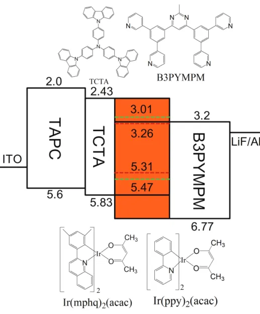
Figure 2.1 (a) The molecular structure of TCTA, B3PYMPM, Ir(ppy)
2(acac), and Ir(mphq)
2(acac), and the device structure and energy level diagram of the OLEDs ... 31
Figure 2.2 (a) The normalized PL spectrum of the TCTA:B3PYMPM co- deposited film and Ir(ppy)
2(acac), and the extinction coefficient of the Ir(ppy)
2(acac), and Ir(mphq)
2(acac). (b) Normalized electroluminescence spectra of the OLEDs at a current density of 10mAcm
-2. ... 32
Figure 2.3 (a) The current density-voltage-luminance characteristics of the OLEDs. Inset shows the angular distribution of the calculated number of photons from the measured EL spectra. (b) The corrected EQE and the power efficiency of the OLEDs. ... 34
Figure 2.4 The EL spectra normalized by the current density of the OLED, at various current densities of 1, 5, 10, and 30 mAcm
-2: (a) 0.3 wt% Ir(mphq)
2(acac), (b) 0.5 wt% Ir(mphq)
2(acac), (c) 1 wt%
Ir(mphq)
2(acac), and (d) 2 wt% Ir(mphq)
2(acac). Inset shows the
xiii
CIE chromaticity coordinates of the OLEDs at the various current densities of 1, 5, 10, and 30 mAcm
-2. ... 37
Figure 2.5 (a) The normalized time resolved electroluminescent characteristics of the OLEDs. Inset shows the magnified transient electroluminescence around the turn-off region. (b) Transient EL signals of the OLED with an Ir(mphq)
2(acac) concentration of 2 wt% after the voltage pulse is turned off and different voltages are applied in the off-state (from – 5 to 2 V).. ... 39
Figure 2.6 The EQE of the red peak portion normalized by the EQE of the red peak portion of the OLEDs at 1 mAcm
-2vs. current density..
... 41
Figure 3.1 (a) Molecular structures of green and red phosphorescent dopants. (b) Angle-dependent PL intensity of the p-polarized light at 520 nm for green (c) at 605 nm for red emissions from the 34- nm-thick TCTA:B3PYMPM:green dopant:red dopant (1:1 molar ratio of co-host:8 wt%:0.4 wt%) and TCTA:B3PYMPM:red dopant (1:1 molar ratio of co-host: 0.4 wt%). Solid lines shows the best fitting curves by the theoretical calculations. ... 47 Figure 3.2 The device structure and energy level diagram of the orange
OLEDs. ... 49
xiv
Figure 3.3 (a) The current density-voltage-luminance characteristics of the orange OLEDs with different green and red dopants in the EML.
Inset shows the angular distribution of calculated number of photons from measured EL spectra, the black solid line is a guide for Lambertian distribution. (b) The calibrated EQEs and power efficiency of the orange OLEDs with increasing luminance. (c) The normalized electroluminescent spectra of the orange OLEDs.
(d) CIE color coordinates for the corresponding spectra shown in (c).. ... 51
Figure 3.4 The schematic diagram of green and red emissions in the exciplex forming co-host with green and red dopant molecules and various kinetic processes such as ISC, RISC, energy transfer (ET), emission, and non-radiative decay are displayed
………... ... 53
Figure 3.5 (a) The transient EL decay intensity at 520 nm for Ir(ppy)3 based orange and green OLEDs (b) for Ir(ppy)2acac based orange and green OLEDs. Solid lines show the best fitting curves with equation (1). ... 55
Figure 4.1 The molecular structure of TCTA, B3PYMPM, Ir(ppy)
2(acac),
and Ir(mphq)
2(acac) and the device structure and energy level of
the OLEDs... ... 63
xv
Figure 4.2 (a) The current density-voltage-luminance characteristics of the OLEDs. (b) The EQE and the power efficiency of the OLEDs.65
Figure 4.3 (a) The un-normalized electroluminescence spectra of OLEDs at the current density of 10 mA/cm
2. The normalized EL spectra of the OLEDs with thicknesses of the red/green EML of (b) 5/25 nm, (c) 10/20 nm, and (d) 15/15 nm, at various current densities. 68
Figure 4.4 (a) The normalized transient electroluminescent characteristics of the OLEDs. The inset shows a magnified transient electroluminescence in the turn-off region. (b) Transient red and green EL signals of the OLED with a thickness of the red/green EML of 5/25 nm after the voltage pulse is turned off with different off-state voltages (from -5 to 0 V). ... 70
Figure 5.1 Energy level diagram and material characteristics of a WOLED.
(a) Hollow boxes represent the LUMO (upper line) and HOMO
(under line) levels of the materials. The orange and blue shaded
boxes represent the HOMO and LUMO levels of the exciplex-
forming co-hosts of the orange and blue EMLs, respectively. The
gray shaded box represents the energy level of the buffer layer
(BL). The dashed lines represent minor quantities in the layers,
with the red, green, blue, and black dashed lines indicating the
energy levels of Ir(mphmq)
2(tmd), Ir(ppy)
2(tmd), FIrpic, and
xvi
B3PYMPM, respectively. (b) Molecular structures of exciplex- forming co-hosts (TCTA, mCP, B3PYMPM) and blue [FIrpic], green [Ir(ppy)
2(tmd)], and red [Ir(mphmq)
2(tmd)] dyes. Φ
PLand
Θ represent the PL quantum yields and average horizontal dipoleratios, respectively, of the three iridium complexes. (c) Triplet energy levels of the dopants, the host materials, and the exciplex of the co-hosts used in the WOLEDs. (d) Angle-dependent PL intensity of the
p-polarized light from the 30-nm-thickTCTA:B3PYMPM:Ir(ppy)
2tmd:Ir(mphmq)
2tmd (1:1 molar ratio of co-host:8 wt%:0.5 wt%) and mCP:FIrpic (10 wt%) film at 470, 520 and 605 nm for blue, green and red, respectively.
Experimental data were fitted by the theoretical calculations (solid lines). ... 76
Figure 5.2 EL spectra and colour quality of the WOLEDs. (a) Electroluminescence spectra measured in the normal direction to the glass substrates at 1,000 cd m
–2. The CRI, the CCT, and the CIE coordinates are given for each spectrum. (b) Photograph of coloured balls illuminated with the light of the WOLED II. . 79
Figure 5.3 Performance and mode analysis of the WOLEDs. (a) Current
density-voltage characteristics of the WOLEDs. Inset shows the
angular distribution of the number of photons calculated from
the measured EL spectra. (b) External quantum efficiencies of
the WOLEDs with/without index matched glass half sphere as a
xvii
function of luminance. (c) Luminous efficacies of WOLEDs with/without index matched glass half sphere as a function of luminance. (d) Mode fraction simulated using classical dipole model for WOLED II. The photoluminescence quantum yields/average horizontal transition dipole ratios of the blue, green, and red emitters of 97/73%, 96/77% and 87/82%, respectively, were used in the simulation. The recombination zone was assumed to be located at the middle of the orange and blue emission layers. The exciton density ratios of the blue, green, and red emitters were assumed to be 0.11, 0.29 and 0.60, respectively, extracted from fitting the measured electroluminescence spectrum of WOLED II shown in Figure 5.2a. The experimentally obtained external quantum efficiencies of the WOLED with/without index matched glass half sphere are included in the figure for comparison. ... 80
Figure 5.4 Comparison of the performance of WOLEDs demonstrated in this work with the state-of-the-art WOLEDs.…...….. ... 82
Figure 5.5 Theoretical and experimental power efficiency of a WOLED (R
0.5 wt%). Theoretical power efficiency using electroluminescence
spectrum shown in Fig. 2a (R 0.5 wt%) as function of an
operating voltage and an external quantum efficiency. A black
solid line is added a guide for eyes, illustrating a power efficiency,
80 lm W
-1, of fluorescent tube. The scatters indicate the calculated
xviii
power efficiencies of air mode only, air mode and substrate mode, and the air mode, substrate mode and waveguide modes. where the minimum operating voltage (2.9 V) as the blue photon energy divided by q (V=hν
blue/q) for the theoretical limits is assumed. Theblack solid lines with scatters and red dashed line with scatters indicate the experimental values without and with the half sphere lens, respectively.…...….. ... 85
Figure 5.6 Normalized time resolved electroluminescent characteristics of the WOLED (R 0.5 wt%). All data were measured using a voltage pulse corresponding to 20 mA cm
–2in the static
J-Vcharacteristics (Figure 5.3a). The detection wavelengths were 468, 524 and 608 nm for the blue, green and red emissions, corresponding to the peak wavelengths of the FIrpic, Ir(ppy)
2(tmd) and Ir(mphmq)
2(tmd) emissions, respectively.
Insets show the magnified transient electroluminescence in the turn-on and turn-off regions.…. ... 87
Figure 6.1 Molecular structures studied in this paper: HATCN, TAPC, NPB, BPhen, B3PYMPM and TPBi. ... 92
Figure 6.2 (a) Linear current density voltage characteristics for different
electron transporting layers. (b) Log-log current density voltage
characteristics for different electron transporting layers (current
density is the absolute value, the filled symbols hold for the
xix
forward bias direction, the open symbols hold for the reverse bias direction, the solid line is added as a guide for the eye, illustrating a slope of 2 which is the dependence expected for the space charge limited current) of samples with glass substrate/patterned ITO (150nm)/TAPC-ReO
3(8 wt%, 30 nm)/HATCN (20 nm)/ETLs-Rb
2CO
3(30 mol%, 20 nm)/B3PYMPM-Rb
2CO
3(15 wt%, 30 nm)/Al (100 nm). ... 95
Figure 6.3 Capacitance voltage characteristics for different electron transporting layers (measured at 1 kHz, and with an applied ac bias voltage of 10 mV) of samples with glass substrate/patterned ITO (150nm)/TAPC-ReO
3(8 wt%, 30 nm)/HATCN (20 nm)/ETLs-Rb
2CO
3(30 mol%, 20 nm)/B3PYMPM-Rb
2CO
3(15 wt%, 30 nm)/Al (100 nm). ... 97
Figure 6.4 Energy level alignment diagrams of the HATCN/Rb
2CO
3doped ETLs at thermal equilibrium, with the condition determined by Capacitance-Voltage measurement. (a) BPhen, (b) B3PYMPM, (c) TPBi, and the schematic energy level alignment diagram of (d) p-TAPC/HATCN/n-BPhen CGU, (e)
p-HTL/n-ETL CGU.102Figure 6.5 The current density - voltage characteristics of the
p-TAPC/HATCN/n-BPhen/n-B3PYMPM charge generation unit
(filled rectangle) and the ITO/p-MeO-TPD (doped with 8 wt %
ReO
3, 15 nm) /n-BPhen (15 wt% doped with Rb
2CO
3, 30 nm)/Al
xx
charge generation unit (filled circle). ... 104
Figure 7.1 (a) The energy level diagram of an orange OLED. (b) Molecular structures of exciplex-forming co-hosts (TCTA and B3PYMPM), green [Ir(ppy)
2(tmd)], and red [Ir(mphmq)
2(tmd)] dyes. Φ
PLand
Θ represent the PL quantum yields and average horizontal dipoleratios, respectively, of the two iridium complexes. ... 109
Figure 7.2 (a) The current density-voltage-luminance characteristics of the orange OLED. Inset shows the angular distribution of the calculated number of photons from the measured EL spectra. (b) The External quantum efficiency and the power efficiency of the orange OLED. (c) Electroluminescence spectrum measured in the normal direction to the glass substrates at 1 mA cm
–2. The CIE is coordinated given for the spectrum. (d) The mode analysis of the orange OLED and the experimentally obtained external quantum efficiency of the orange OLED is included in the figure for comparison. ... 111
Figure 7.3 (a) Schematic tandem WOLEDs structure consisted of blue emitting unit, orange emitting unit by conjunction with charge generation unit. (b) The mode analysis of blue light as a function of the thickness of HATCN at total HTL thickness of 80 nm.
Mark ( ) shows the thickness of HATCN when an out-coupled
mode is maximized. (c) The mode analysis of white light as a
xxi
function of the thickness of total HTL at HATCN thickness of 40 nm and the experimentally obtained external quantum efficiencies of the tandem WOLEDs with/without index matched glass half sphere are included in the figure for comparison. (d) The mode analysis of white light as a function of the thickness of HATCN at total HTL thickness of 80 nm and the experimentally obtained external quantum efficiencies of the tandem WOLEDs with/without index matched glass half sphere are included in the figure for comparison. ... 112
Figure 7.4 (a) The energy level diagram of a blue OLED. (b) Molecular structures of exciplex-forming co-hosts (mCP and B3PYMPM), blue [FIrpic)] dye. Φ
PLand Θ represent the PL quantum yield and average horizontal dipole ratio, respectively, of FIrpic. 114
Figure 7.5 (a) The current density-voltage-luminance characteristics of the
blue OLED. Inset shows the angular distribution of the
calculated number of photons from the measured EL spectra. (b)
The External quantum efficiency of the blue OLED. (c)
Electroluminescence spectrum measured in the normal direction
to the glass substrates at 1 mA cm
–2. The CIE is coordinated
given for the spectrum. (d) The calculated EQE as a function of
ETL thickness and the experimentally obtained EQE of the blue
OLED with ETL thickness of 55 nm. ... 115
xxii
Figure 7.6 The mode analysis is performed the device structure shown in Figure 2 (a) at fixed HATCN thickness of 40 nm. (a) Out-coupled mode (b) Substrate guided mode (c) ITO/Organic guided mode (d) Surface plasmon loss mode for blue, green, and red light, respectively, as a function of total HTL thickness. ... 116
Figure 7.7 (a) The current density-voltage-luminance characteristics of the tandem WOLEDs. Inset shows the angular distribution of calculated number of photons from measured EL spectra (b) The External quantum efficiency and the power efficiency of the tandem WOLEDs. ... 118
Figure 7.8 (a) Electroluminescence spectrum measured in the normal
direction to the glass substrates at 1 mA cm
–2. (b) The CIE
coordinates of blue, orange, and tandem white OLEDs for the
given spectra in Figure 7.8a at 1 mA cm
–2. (c) The normalized
electroluminescence spectra of tandem WOLED II with
increasing current density from 1 to 10 mA cm
–2. ... 120
1
Chapter 1. Introduction 1.1 Organic light emitting diodes
Organic light-emitting diodes (OLEDs) have great potential for application in displays, lights, automobiles, imaging, and medicine. High quality characteristics such as flexibility, transparency, light weight, thin form factor, etc, and the sheer multi- functionality of OLEDs have convinced many researchers around world to explore the potential of high performance OLEDs over the last several decades.
The first electroluminescence (EL) was observed in inorganic semiconductors by H. J.
Round in 1907, when light was emitted from a Silicon carbide (SiC) crystallite.1 Lossev reported detailed investigations of the EL phenomena observed from metal- SiC semiconductor rectifiers in 1928.2 From these pioneering findings, the III-V compound semiconductors such as GaAs, GaP, GaN, AlGaAs, GaAsP, GaInN, and AlGaInP, etc were investigated for use as LEDs. However, inorganic LEDs were composed of materials in the form of single crystals that were fabricated by epitaxial growth on single crystal substrates. Therefore, it is difficult to fabricate large-size LEDs with a low cost. In addition, an inorganic semiconductor is usually processed at a high temperature or via a toxic chemical-etching process, neither of which are favorable when trying to reduce energy usage or create environmentally-friendly devices.
The organic materials were well known for multi-functionality and low- fabrication cost. The pioneering discovery of electrically conducting polymers won A. G.
MacDiarmid, H. Shirakawa, and A. J. Heeger a Nobel Prize in Chemistry in 2000. In 1965, the first EL in organic semiconductors was observed on antracene single
2
crystals.3 However, their efficiency was very low. The breakthrough came in the form of a heterojunction OLED design consisting of a hole transporting layer (HTL) and an emitting layer (EML), which was also used for an electron transporting layer (ETL) through the thermal evaporation of small molecules under high vacuum by C. Tang and S.A. VanSlyke.4 Meanwhile, a breakthrough on the material side was reported by J. H. Burroughes et al. using conducting polymers for LEDs called polymer light- emitting diodes (PLED).5 The relative ease of processing of the organic compounds using methods such as thermal deposition,4 spin coating,5 ink-jet printing,6 laser induced thermal imaging,7 and roll-to-roll process8 as well as the formation of organic films on a variety of very low cost substrates such as glass, plastic or metal foils enabled human-friendly electronic devices such as flexible, transparent, and wearable electronic devices.9 In particular, small molecular organic semiconductors have been widely used in mobile displays using the technique of thermal evaporation using a fine shadow mask and are now being extended to the large-size displays using the same fabrication method or a white OLED with pre-patterned color filter arrays on active-matrix thin film transistor substrates.
As mentioned previously, OLEDs can be used variety of applications. Among them, OLEDs were the most successfully applied in display industry. There are a lot of advantages of using OLEDs in displays: (1) OLEDs have very simple structure consisting of several organic layers sandwiched between two electrodes compared with existing display systems such as liquid crystal display (LCD) or plasma display panel (PDP); (2) OLEDs have a good color quality (high color gamut, good viewing angle properties), light weight, and flexibility; and (3) OLEDs are environment- friendly devices due to their potentially high luminous efficiency because it only emits light on the active pixel. By contrast, LCDs use a back light unit, shutter the light on
3
or off using an LC switch, and filter the light to get the proper colors for full color display applications. These advantages could help the commercialization of OLEDs succeed for such devices as the high quality displays used for smart phones, digital cameras, curved smart phones, and curved televisions.
Aside from displays, one of the largest markets for OLEDs is light sources. Lighting equipment is responsible for 17% of global electricity consumption, with over 90% of that being consumed by conventional light sources such as incandescent lamps, compact fluorescent lamps, and fluorescent tubes.10 However, the efficiency of these conventional light sources are already limited (~17 lm W-1 for incandescent lamps and
~90 lm W-1 for fluorescent tubes) by fundamental factors.11 Therefore, OLEDs with a high luminous efficacy should be developed to replace these conventional light sources to reduce energy consumption as well as carbon emissions. In addition, white OLEDs are considered to be a more attractive light source than traditional lights including LEDs in terms of the quality of their light, their flexibility, and so on.
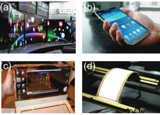
Figure 1.1 shows the commercially available products and currently developing applications that use OLEDs such as a curved OLED TVs, curved smart phones, transparent displays, and light sources. This ubiquity of OLEDs in electronic devices indicates that there will be wide range of applications using organic semiconductors in near future.
4
Figure 1.1 (a) Curved television (LG Display 2013). (b) Curved smart phone (Samsung Display 2013). (c) Transparent OLED display (Samsung Display 2011). (d) OLED flexible lighting (LG chem. 2013).
5
1.2 Operating principles of organic light-emitting diodes
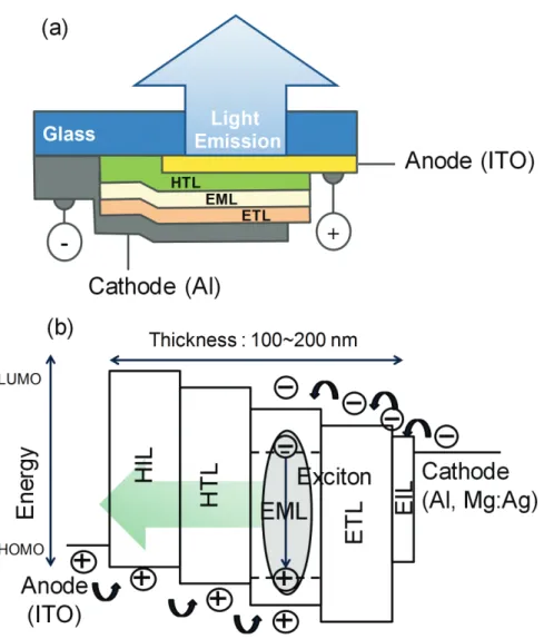
1.2.1 Basic device configurations and functional layers
The basic architecture of a typical bottom-emitting OLED is shown in Figure 1.2a. A bottom emitting OLED consists of a transparent anode on top of a glass substrate, followed by hole transport layer (HTL), emitting layer (EML), electron transporting layer (ETL), and a reflective metallic cathode, finally capped with hermetic encapsulation for a higher operating stability in an inert environment. The first efficient OLED consisting of a two layered structure was introduced by C. Tang and S.
A. VanSlyke4. The functional layers were introduced to enhance the device’s efficiency and operating stability. Currently, highly efficient OLEDs have become complex multilayer structures, where various functions for instant charge transporting, exciton formation, energy transfer, recombination, and so on, are separated to achieve theoretical device efficiency. The physical processes in a multi-layered OLED are schematically illustrated in Figure 1.2b; (1) injection of holes from a high work function anode (the transparent metal oxide, indium thin oxide (ITO), are mostly used in the bottom emission configuration) into the highest occupied molecular orbital (HOMO) of a HTL through a hole injection layer (HIL, this layer is used to reduce the injection barrier from the anode to the HTL as well as enhance the device’s stability by increasing the device’s life time and reducing short-related sudden breakdowns) and electrons from cathode into the lowest unoccupied molecular orbital (LUMO) of an ETL through an electron injection layer (EIL, this layer is used to reduce injection barrier from a cathode to an ETL), (2) transport of the oppositely charged carriers through a HTL and an ETL towards an EML each other under the applied electric
6
Figure 1.2 (a) The basic architecture of a typical bottom emitting OLED. (b) The schematic physical processes in a multi-layered OLED.
7
field; both a HTL and an ETL are important to achieve high device efficiencies and have three key functions: (i) high hole mobility for a HTL and electron mobility for an ETL are required to reduce voltage drops in the layers, (ii) the higher LUMO energy level of a HTL and the lower HOMO level of an ETL than those of the EML are required to effectively confine the electron-hole charge carriers in the EML to reduce the electron-hole leakage current, (iii) for phosphorescent emitting systems, the triplet energy of both layers is higher than that of the emitter to confine the triplet excitons in the emitter because triplets have a long decay time (order of µs), which increases their diffusion into adjacent layers (3) injection holes and electrons into an EML from a HTL and an ETL, respectively, and transport of the oppositely charged carriers across the an EML towards each other under the electric field, (4) recombination of the oppositely charged carriers in the EML forming an exciton, (5) energy transfer into dopants from hosts, this process is an optional one where the host-guest system is used in the emitter, and then (6) subsequent radiative decay of formed excitons. These processes have been intensively studied.
1.2.2 Intermolecular energy transfers
In the emitter system, neat film can be used as an emitter; however, the concentration quenching reduces the efficiency of the device. Therefore, a host–guest system is preferred because the functions for host and guest can be divided into respective materials. The host materials form amorphous, disordered films that have a high glass transition temperature and polar or bi-polar charge transport properties. In addition, the host materials should have a higher singlet energy for fluorescent emitter and triplet energy for phosphorescent emitter than dispersed guest molecules. In contrast,
8
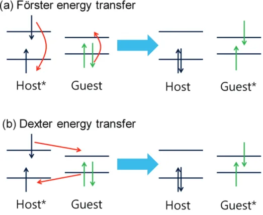
guest materials should have high photoluminescent (PL) quantum yields (QYs) and be uniformly dispersed in the host molecules. The energy transfers into a guest from a host material are of central importance in OLEDs. There are two main categories for non-radiative energy transfer, Förster energy transfer and Dexter energy transfer.
Figure 1.3 shows the schematic diagrams for Förster energy transfer and Dexter energy transfer. In Förster energy transfer, the rate constant of the energy transfer process can be described by the equation (1)12
(1) where ν is the wave number; εG(ν) is the molar extinction coefficient of the guest;
fH(ν) is the spectral distribution of fluorescence (measured in quanta and normalized to unity on a wave number scale); NA is Avogadro’s number; φPL,H is fluorescent QY of host molecules; τH is the radiative lifetime of host molecules; n is the refractive index of medium; R is intermolecular distance between host and guest molecules; R0 is the critical transfer distance (called the Förster transfer radius) for which excitation transfer and spontaneous decay of the host are of equal probability; and κ is an orientation factor. More specifically, this is expressed by the equation (2) 12
(2) Where φHG is the angle between the transition moment vectors of both molecules and φH and φG are the angles between these respective vectors and the direction H G.
The average value for a random directional distribution is κ2=2/3. The Förster energy transfer is dipole–dipole interaction, therefore, a long-range process, in a typical case Förster energy transfer can occur up to 100 Å.12,13 singlet–singlet and singlet–triplet energy transfer are possible through the Förster mechanism.12 In Dexter energy
6 6 0
4 0
5 2 ,
( ) ( ) 1 1
128 ) 10 (ln
9
=
= N n
∫
∞ f d R RRk
H H
G H A
H
F PL
ν ε ν ν τ τ
π φ κ
G H
HG
φ φ
φ
κ = cos − 3 cos ⋅ cos
9
Figure 1.3 The schematic diagrams for (a) Förster energy transfer and (b) Dexter energy transfer.
10
transfer, the exciton hops directly between molecules; therefore, this is a short-range process. In a typical case, Dexter energy transfer can occur over 10 to 15 Å, dependent on the overlap of the molecular orbitals of neighboring molecules.13, 14 Dexter energy transfer is suppressed when the doping concentration is low enough due to the long average distance between host and guest molecules. It is allowed by the Dexter energy transfer between singlet–singlet and triplet–triplet energy transfer.
1.2.3 Charge balance factor and prediction of efficiency in organic light emitting diodes
The external quantum efficiency (EQE) of OLEDs is one of the most important factors. The definition of EQE is the number of emitting photons per injected electrons. The EQE is simply composed of a charge balance factor (γ), radiation allowed exciton ratio (
η
S/T), the effective radiative quantum yield (qeff) of the emitter in the cavity structure and the out-coupling efficiency (η
out). Equation (3) well describes the EQE (η
EQE) of OLEDs.15(3) The EQE of OLEDs can been improved by maximizing each factor in equation (3).
This can be achieved by introducing heavy metal complexes and pushing the maximum radiation allowed exciton ratio from 25% up to 100% through charge carrier spin statistics.16 A host–guest system in EML reduces the self-quenching between dye molecules and enhances the radiative quantum yield.17,18 Out-coupling efficiency is maximized with an optimized thickness of transparent conducting oxide (TCO)19 and proper selection of dopant materials that show horizontal dipole
out eff T S
EQE
γ η q η
η = ×
/× ×
11
Figure 1.4 (a) The schematic device structure with with hole current (Jh), electron current (Je), leakage current (Je’ and Jh’), recombination current (Jr), and total current (J). (b) The schematic illustration of charge balance factors with various situations of electron, hole, and recombination currents.
12
orientation because the out-coupling efficiency of horizontal dipoles is higher than that of vertical dipoles.15 Figure 1.4a shows a schematic device structure with hole current (Jh), electron current (Je), leakage current (Je’ and Jh’), recombination current (Jr), and total current (J). The relationships of charge balance factor as functions of Jr
and J are shown in the inset of Figure 1.4a. The results are in Figure 1.4b, which is a schematic illustration of charge balance factors with various situations of electron, hole, and recombination currents. The charge balance in an OLED is highly important and there have been lots of attempts to enhance it, particularly by controlling the charge injection, transport, and confinement in OLEDs. Electrical doping in transporting layers was implemented in so called, p−i−n OLEDs, which demonstrated a lower operating voltage and the charge balance was optimized with EML thickness and a proper choice of hole blocking layer (HBL).20-22 Hole or electron injection was improved to obtain better charge balance in OLEDs by using a graded hole-transport, an insulating layer, a chlorinated ITO, transition metal oxides, a self assembled monolayer, alkali metal halides, and metal carbonates.23-28
It is important to note that qeff is a function of the photoluminescence (PL) quantum yield, φPL, the horizontal-to-vertical dipole ratio,
Θ ≡ ( p
∥/ p
∥+ p
∥)
, wherep
∥and
p
∥ represent the proportion of horizontal and vertical dipoles, respectively, and the structure of the microcavity including the position of the emission zone is represented by Γ. The out-coupling efficiency,η
out , also depends on Θ and Γ. Therefore, the equation (3) can be modified to equation (4) 29(4)
All the factors are categorized into two main parts: One is the device-related characteristics composed of γ and Γ and the other is the material-related characteristics
) , ( )
, ,
/
× ( Θ Γ × Θ Γ
×
=
S T eff PL outEQE
γ η q φ η
η
13
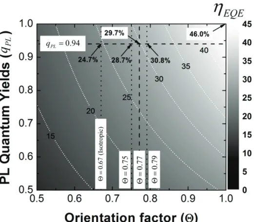
Figure 1.5. Contour plot of the simulation results of EQE as a function of qPL and Θ . The two dashed lines indicate the locus of the EQE for Θ = 0.77 and qPL = 0.94, respectively. In a similar manner, the dotted lines indicate the EQE for Θ = 0.67 (isotropic), 0.75, and 0.79, respectively.29
14 composed of
η
S/T,q
eff , and Θ.A very important conclusion can be reached here, which is that it is possible to universally predict the maximum EQE of OLEDs using Θ andφPL. Figure 1.5 shows the predicted EQEs of OLEDs as functions of Θ andφPL with the following structure:
ITO (70 nm) / TAPC (75 nm) / TCTA (10 nm) / TCTA:B3PYMPM:Ir(ppy)2acac (30 nm, 8 wt%) / B3PYMPM (40 nm) / LiF (0.7 nm) / Al (100 nm), where TAPC, TCTA, B3PYMPM, Ir(ppy)2acac. The maximum EQE increases as qPL and Θ approach 1 as expected. Surprisingly, a maximum EQE of 46% can be achieved in normal ITO-based bottom-emitting OLEDs without any extra out-coupling layers using a phosphorescent dye with φPL = 1 and Θ = 1. In addition, by measuring the Θ andφPL of a phosphorescent dye, we can universally predict the maximum achievable EQE of an OLED having the phosphorescent dye using this contour plot.29
1.3 Exciplex-forming co-hosts for organic light-emitting diodes with ultimate efficiency.
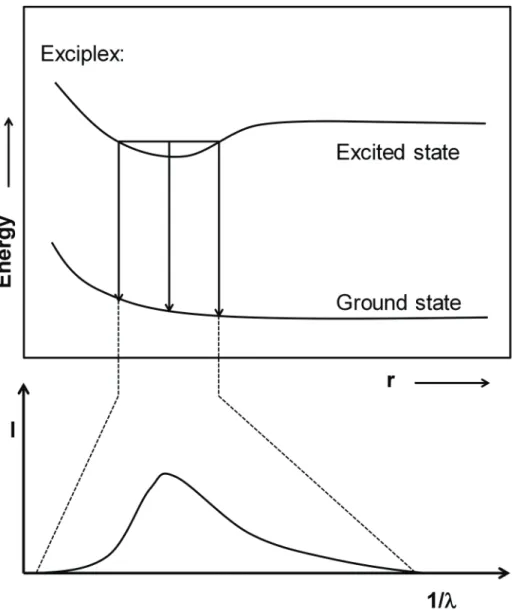
In organic semiconductors, the electronic excited states are different from those in inorganic semiconductors. Organic semiconductors are van der Waals force-bonded solids, therefore, the molecular (localized) exciton model is applicable.30 In contrast to the Mott-Wannier excitons in a tightly bonded inorganic semiconductor, the binding energy of excitons in an organic semiconductor is high enough. At room temperature, excitons are localized and their migration can be described as a random walk that can be described by diffusion formalism. Figure 1.6 shows several different excitons with different binding energy.30 Wannier excitons have not been seen in organic semiconductors. Frenkel excitons are the limiting case of excitonic excited states in
15
Figure 1.6 Excitons with different fadii: diagram of (a) a Frenkel exciton, (b) a Wannier exciton, and (c) a charge-transfer (CT) exciton.30
16
Figure 1.7 Potential energy diagram correlating the spectral region of the emission band I(λ) with the intermolecular distance.31
17
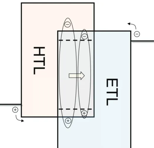
which the correlated electron-hole pair is localized on the same molecule and can move through the lattice in this form. 30 On the other hand, two kinds of bimolecular excitonic excited states also exist in the form of excited charge transfer excitons. One is an excited dimer (so called excimer), the other is an excited complex (so called exciplex). This molecular complex may be dissociated in the ground state, and yet be associated in an excited electronic state.32 A potential energy diagram correlating the spectral region of the structureless emission band I (λ) with intermolecular distance is shown in Figure 1.7.31 When donor and acceptor molecules approach each other, steric hindrance will repel, therefore, it is dissociative at ground state. However, when one of the molecules is excited (D* or A*), the bonding between D and A molecules may increase as the two molecules approach due to the charge transfer interactions of excited states. Therefore, an excited electronic state is associative. The exciplex- forming co-hosts were proposed for a system that overcomes all the barriers to realizing the ultimate efficiency in OLEDs in terms of the EQE, driving voltage and the efficiency roll-off.33 Figure 1.8 shows the schematic device structure with energy diagram using an exciplex-forming co-host composed of a hole transporting material (HTM) and an electron transporting material (ETM), which are used for a HTL and an ETL, respectively.33 In this system, (1) electrons and holes reach the co-host EML without energy barriers via the ETM and HTM, respectively; (2) the recombination of the oppositely charged carriers in the EML form an exciplex with a wide recombination zone, which induces a low polaron density and low triplet-polaron quenching; (3) efficient energy transfer into phosphorescent dyes from exciplex where the electrons and holes in the co-host are well confined inside the EML due to very high injection barriers between the HTL/EML for electrons and the EML/ETL for holes, while the triplet energies of the HTL, ETL, and exciplex are higher than that of
18
Figure 1.8 The schematic device structure with energy diagram using an exciplex- forming co-host composed of a hole transporting material (HTM) and an electron transporting material (ETM) as well as the HTM and ETM are used for a HTL and an ETL
19
dyes, therefore the excitons formed in the EMLs are efficiently confined in a co-host doped with phosphorescent dyes; and then (4) the subsequent radiative decay of formed excitons.33
1.4 White organic light-emitting diodes
White organic light-emitting diodes (WOLEDs) have tremendous benefits for light sources, automobiles, large size displays, ultra-high resolution displays, imaging, and medicine. In particular, light sources using WOLEDs have many advantages against fluorescent tubes such as high Color rendering index (CRI), warm color temperature, environmental benefits, and are free from flickering, mercury, glare, and ultra violet (UV) emission. The CRI of WOLEDs is particularly high, which is important for their application in light sources; premium light sources require a CRI higher than 80.
Since the first multilayer architectures for bright WOLED were reported in 199534, great advances have been made in the development of advanced architectures for efficient WOLEDs.34-48
To To produce an ideal white light, a WOLED should emit the entire visible spectrum, however, the EL spectrum from an organic dye is limited to a range of 50–100 nm at full width at half maximum (FWHM). Therefore, several color lights should be mixed; three primary colors or two complementary colors such as blue and orange.
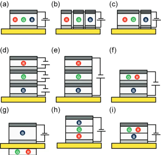
Figure 1.9 shows the various device architectures used to produce a high quality white light emission using the three primary colors. A single EML doped with red, green, and blue phosphorescent dyes WOLED35 [Figure 1.9a, in 2004] can make a high-quality white color, but, it is difficult to control balanced white emission due to the doping concentration being too low. The white light can be produced by side-by-
20
Figure 1.9 The various device layouts to realize high quality white color emission. (a) Single EML doped with red, green, and blue phosphorescent dyes. (b) Side-by-side structures with red, green, and, blue pixels. (c) Side-by-side structures with blue and orange (red and green colors are mixed to emit orange color light) pixels. (d) Vertically stacked OLEDs, blue OLEDs with downconversion layers. (e) Tandem WOLEDs using three primary color emitting unit devices. (f) Tandem WOLEDs using two complementary color unit devices. (g) Blue OLEDs with downconversion layers. (h) Multiple-doped emission layers (EMLs). (h) The multi-EML structure with three EMLs. (i) The multi-EML structure with two EMLs. R, G, and B stand for red, green, and blue dopants, respectively.
21
side structures with red, green, and, blue pixels [Figure 1.9b] or blue and orange (red and green colors are mixed to emit orange color light) pixels [Figure 1.9c]. Vertically stacked OLEDs [Figure 1.9d, in 1996] are ones where each complete red, green, and blue OLED was stacked on top of each other using semi-transparent anodes and cathodes with an external power source.36 This structure is complicated and needs many electrical contacts, which can makecurrent leakage problems in the OLEDs.
Tandem WOLEDs using three-primary-color emitting unit devices37 [Figure 1.9e, in 2008] or two complementary color unit devices38 [Figure 1.9f, in 2003] are one of the most innovative OLED structures because they can increase the efficiency, increasing the device’s working life time. However, the structure is complicated and the driving voltage is high. Blue OLEDs with external or internal downconversion layers can also possibly produce white light [Figure 1.9g]. The most popular structure for producing high quality white light is the WOLEDs with multi-EML structures with three EMLs39 [Figure 1.9h] or two EMLs40 [Figure 1.9i].
It is important to evaluate WOLEDs in terms of efficiency and color quality. Device efficiency is of central importance when evaluating WOLEDs. Luminous efficacy (called power efficiency or power efficacy in practice), the integrated light output divided by the input power, is the most important parameter for a device. It is directly related to the power consumption of the devices. However, it is a photometric value;
therefore, it depends on the color of light. The other important parameter is an EQE, the number of emitting photons per injected electron, which is independent to the color of the light. Therefore, it is frequently used as yardstick with which various WOLEDs emitting different colors can be directly compared.
In addition, the spectral color quality can be evaluated through three important parameters, the correlated color temperature (CCT), Commission Internationale
22
d’Eclairage (CIE) coordinates, and the color rendering index (CRI). These three parameters are closely related. The color temperature of the light emitted from an ideal black body is defined as its surface temperature in Kelvin, however, the light emitted from specific human-made light source is different from the ideal black body radiation. These light sources are designated as CCTs. CCT is the color temperature of a black body radiator in which the human color perception most closely matches the light from the light source. This human color perception of the emission color of any light source (with an arbitrary emission spectrum) can be described by the CIE coordinates. The CRI is represented by a number from 0 to 100 and is a quantitative measure of the ability of a light source to reproduce the colors of various objects faithfully in comparison to an ideal black body radiation or natural light source.
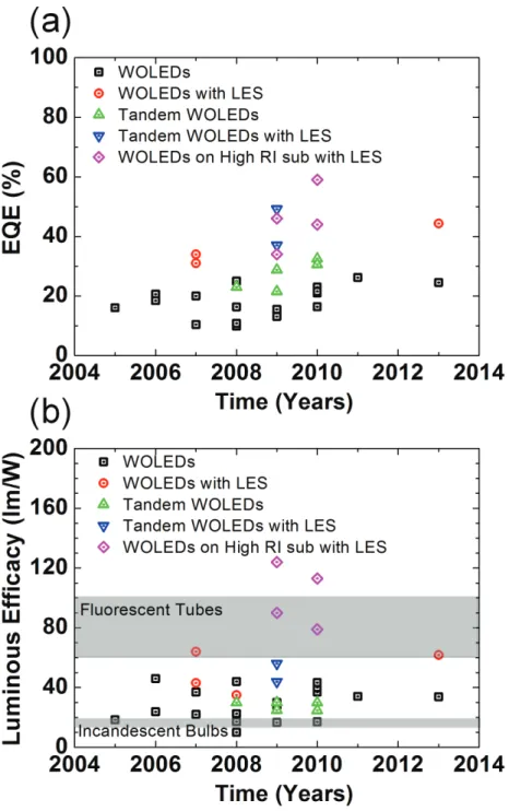
The device efficiency was improved by advancing WOLED architecture schematically as described by Figure 1.9 over two decades. The records for the state- of-art improvement of device efficiencies (luminous efficacies and EQEs) over past 10 years are summarized in Figure 1.10 with the luminous efficacy of incandescent lamps (~15 lm W-1) and fluorescent tubes (60–100 lm W-1). The devices are divided into five different categories: WOLEDs, WOLEDs with light extraction structure (LES), tandem WOLEDs, tandem WOLEDs with LES, and WOLEDs on high refractive index substrate (RIS) with LES. The luminous efficacy achieved in laboratory conditions using WOLEDs overcame that of incandescent lamps in 200541 and using WOLEDs on high RIS with LES overwhelmed that of fluorescent tubes in 2009.39 Currently, the highest EQEs (luminous efficacies) of WOLEDs, WOLEDs with LES, tandem WOLEDs, tandem WOLEDs, and WOLEDs on high RIS with LES were 26.2%42 (43.3 lm W-1)43, 44.3%44 (64 lm W-1)45, 32.5% (30 lm W-1)46, and 49.2%
(56 lm W-1)40, and 59%48 (124 lm W-1)39, respectively. However, the detailed device
23
Figure 1.10 The records for the-state-of-art improvement of device efficiencies (luminous efficacies and EQEs) over the past 10 years (a) EQEs, (b) The luminous efficacies with the luminous efficacy of incandescent lamps (~15 lm W-1) and fluorescent tubes (60–100 lm W-1).
24
structures that were reported in conference papers by companies were not fully revealed.41, 45-48 In addition, the achieved device efficiencies were still not as much as the theoretical limit of WOLEDs. Therefore, ongoing attempts to develop advanced device architectures for WOLEDs are still needed.
1.5 Outline of thesis
In this thesis, orange OLEDs and WOLEDs using exciplex-forming co-hosts as well as tandem WOLEDs with an efficient charge generation unit are developed and the device characteristics are investigated with various analysis tools such as current- density–voltage–luminance (J–V–L) measurement, transient EL, capacitance-voltage (C–V) measurement, and optical calculation using the classical dipole model.
Orange OLEDs with co-doping of green and red phosphorescent dopants in an exciplex-forming co-host are investigated. Orange OLEDs with high efficiency, low driving voltage, and an extremely low efficiency roll-off are achieved and demonstrate an unprecedentedly efficient orange OLED exhibiting the maximum EQE of 32.2%
using green and red phosphorescent dopants with high Θ andφPL in the exciplex- forming co-host. The origin of the color shift is speculated by the concentration bleach due to low red doping concentration using static EL spectra analysis. In addition,the dominant recombination type is the energy transfer (ET) from green to red dopants, which is analyzed using transient EL analysis in a decay region (CHAPTER 2 and 3) High efficiency and non–color-changing orange OLEDs with separated red and green EMLs using an exciplex-forming co-host are investigated. The OLED shows a maximum external quantum efficiency (EQE) of 22.8%; a low roll-off of efficiency with an EQE of 19.6% at 10,000 cd/m2; good orange color with a CIE coordinate of
25
(0.442, 0.529); and no color change from 1,000 to 10,000 cd/m2 (CHAPTER 4).
High quality WOLEDs with a luminous efficacy of over 100 lm W–1 are reported by combining exciplex-forming co-hosts, horizontally oriented phosphorescence dyes, two emission layers for three color white emission, and attaching an index-matched glass half sphere to the conventional glass substrate (CHAPTER 5).
The mechanism of charge generation in charge generation units composed of p-doped HTL / 1,4,5,8,9,11-hexaazatriphenylene hexacarbonitrile (HATCN) /n-doped ETLs is investigated. Energy level alignment is determined by the C-V measurements and the J-V characteristics of the structure that clearly show that the electron injection at the HATCN/n-ETL junction limits the charge generation in the CGUs rather than charge generation itself at the p-HTL/HATCN junction (CHAPTER 6).
Tandem WOLEDs with an EQE approaching the theoretical limit are reported by interconnecting high-efficiency orange OLEDs with the co-doping of green and red phosphorescent dopants that have high Θ andφPL in exciplex-forming co-hosts (concept shown in chapter 2, 3) and a blue OLED using exciplex-forming co-hosts with an efficient CGU (shown in chapter 6). A tandem white OLED (WOLED) with a high maximum EQE of 54.3% (PE of 63 lm W–1), EQE of 52.6% (PE of 52 lm W–1) at 1,000 cd m–2, low efficiency roll-off, and high color stability was demonstrated. In addition, an EQE of 90.6% at 1,000 cd m–2 was achieved by attaching an index- matched glass half sphere on conventional glass substrate (CHAPTER 7).
26
Chapter 2. Orange Organic Light Emitting Diodes with Controlled Co-doping of Green and Red
Phosphorescent Dopants in an Exciplex forming Co- host
2.1 Introduction
Orange emitting organic light emitting diodes (OLEDs) are important in order to achieve highly efficient hybrid tandem white OLEDs, in which a blue fluorescent (FL) and an orange phosphorescent emitting system are connected by using a charge generation unit.49 These hybrid tandem white OLEDs take advantage of a stable blue fluorescent unit with a long device lifetime and a high efficiency orange phosphorescent unit, and are the most widely used structure for displays and solid state lighting. There are two possible ways to construct an orange phosphorescent OLED. One way is to utilize a single orange emitting phosphorescent material. The other way is to utilize both green and red emitting phosphorescent materials. The first method has the advantages of easy fabrication and color stability with increasing luminance over the second method. Various heavy metal complexes which emit an orange color have been reported, based on platinum, iridium, and osmium as the heavy metal.42, 50-55 However, it is difficult to synthesize an orange emitting phosphorescent dye covering both the green and red regions of the spectrum, resulting in a low color rendering index (CRI) and a low color gamut (CG) when combined with a blue emission in white OLEDs. For instance, a very high efficiency orange OLED with an EQE of 27.5% showed a CRI value of 64 when combined with blue.42 Solid state lighting and display applications require that the CRI and CG be over 80
27 and 80% of the NTSC standard, respectively.
The combination of green and red emissions leads to an orange emission with a broad spectrum. In other words, a co-doped green and red dopant in a single emitting layer can be considered as an orange emitter with a broad emission spectrum covering from green to red. Moreover emitting color can be tuned from green to red by adjusting their doping ratio. This quasi orange emitter results in white OLEDs with high CRI values compared to white OLEDs with just one type of orange emitting molecule when combined with a blue emitting layer. Large numbers of tandem white OLEDs incorporating orange OLEDs have been reported where green and red phosphorescent dyes are doped in a single emission layer (EML). Unfortunately, however, there are only a limited number of papers on the orange OLEDs themselves and their EQE values were less than 17.6% to our best knowledge.56-58 Most of the works dealing with orange OLEDs are focused on assembled white OLEDs, and the orange OLEDs were not themselves studied in detail. Moreover, compared to the importance of orange OLEDs