• 검색 결과가 없습니다.

Low-temperature Epitaxial Growth of a Uniform Polycrystalline Si Film with Large Grains on SiO2 Substrate by Al-assisted Crystal Growth

N/A
N/A
Protected

Academic year: 2021

Share "Low-temperature Epitaxial Growth of a Uniform Polycrystalline Si Film with Large Grains on SiO2 Substrate by Al-assisted Crystal Growth"

Copied!
6
0
0

로드 중.... (전체 텍스트 보기)

전체 글

(1)

1. Introduction

Saving the fabrication cost of crystalline silicon is one of the important tasks to reduce material costs in Si solar cells. One possible approach to reach this goal might be epitaxial growth of thin Si film on glass substrate so that the fabrication cost of Si wafer by crystal growing, slicing, and polishing can be eliminated.

Solid phase crystallization (SPC) of an amorphous Si film has been approached to grow a polycrystalline silicon (poly-Si) film for low-cost solar cells

1,2)

. But the grain size of the Si film with the SPC process is too small. Al induced crystallization (AIC) of a-Si film was employed to increase the grain size of Si film

3,4)

. However, the thickness of Si film grown by the process ranges from 50 to 100 nm, which is too thin to be used for Si solar cells

5,6)

. We need thicker film with a large grain sizes. For the thick film, a poly-Si film grown by AIC process was used as seed layer and an epitaxial Si film with a thickness of 2 to 6 μm was grown at 1,130°C by hot wire chemical vapor deposition on

alumina substrate

7,8)

. The highest conversion efficiency of the Si solar cell with the film was close to 11%

9,10)

.

We utilize the same AIC process for the growth of epitaxial Si. We grow an epitaxial Si film at low temperature (450°C) instead of high temperature (1,100°C). For the epitaxial growth, Si source is continuously supplied from SiH

4

gas, not from a-Si.

The Si supplied from SiH

4

gas will be dissolved in the Si-Al solid solution layer and precipitated on the existing Si crystal.

As a result, it is expected that a thick epitaxial Si film can be grown at low temperature by Al-assisted crystal growth.

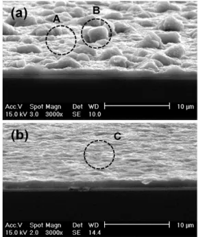
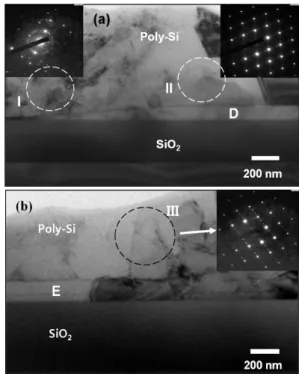
It was found that the epitaxial growth of Si film on Al metal layer resulted in a severe surface roughness with uncontrollable Al contamination. To reduce the surface roughness, we introduced a thin a-Si layer on the Al metal layer as a crystal Si seed layer.

As a result, the surface roughness was much improved and the crystallinity of the film was also greatly improved.

2. Experimental

A SiO

2

-grown p-type Si (100) wafer and Corning glass was used as substrates. The silicon oxide was grown by wet oxidation at 1,050°C to a thickness of 500 nm to prevent

Low-temperature Epitaxial Growth of a Uniform Polycrystalline Si Film with Large Grains on SiO 2 Substrate

by Al-assisted Crystal Growth

Kyung Min Ahn

1,2)

․ Seung Mo Kang

1)

․ Seon Hong Moon

1)

․ HyukSang Kwon

1)

․ Byung Tae Ahn

1)

*

1)

Department of Materials Science and Engineering, Korea Advanced Institute of Science and Technology, Yuseong-gu, Daejeon 305-701, Korea

2)

Present address: GS Caltex R&D Center, Yuseong-gu, Daejeon 305-380, Korea

ABSTRACT: Epitaxial growth of a high-quality thin Si film is essential for the application to low-cost thin-film Si solar cells. A polycrystalline Si film was grown on a SiO

2

substrate at 450°C by a Al-assisted crystal growth process. For the purpose, a thin Al layer was deposited on the SiO

2

substrate for Al-assisted crystal growth. However, the epitaxial growth of Si film resulted in a rough surface with humps. Then, we introduced a thin amorphous Si seed layer on the Al film to minimize the initial roughness of Si film. With the help of the Si seed layer, the surface of the epitaxial Si film was smooth and the crystallinity of the Si film was much improved. The grain size of the 1.5- μm-thick Si film was as large as 1 mm. The Al content in the Si film was 3.7% and the hole concentration was estimated to be 3 × 10

17

/cm

3

, which was one order of magnitude higher than desirable value for Si base layer. The results suggest that Al-doped Si layer could be use as a seed layer for additional epitaxial growth of intrinsic or boron-doped Si layer because the Al-doped Si layer has large grains.

Key words: Si film, crystalline Si film, Al-assisted crystal growth, epitaxial growth, large grains

*Corresponding author: [email protected]

Received November 25, 2013; Revised November 29, 2013;

Accepted December 4, 2013

ⓒ 2013 by Korea Photovoltaic Society

This is an Open Access article distributed under the terms of the Creative Commons Attribution Non-Commercial License (http://creativecommons.org/licenses/by-nc/3.0)

which permits unrestricted non-commercial use, distribution, and reproduction in any medium, provided the original work is properly cited.

103

(2)

any crystalline orientation effect of the Si substrate. After an RCA cleaning process, the substrate was placed in a DC sputtering chamber. An aluminum layer with various thicknesses in the range of 20 and 250 nm was deposited. The substrate temperature and chamber pressure were kept at room temperature and 5 mTorr, respectively. After the Al deposition, the samples were removed from the sputtering system and loaded into a hot wire CVD (HWCVD) system. Epitaxial Si films with a thickness of 1.5 μm were then grown on the substrates by HWCVD at 450°C for 1 h. The flow rate of Ar-diluted 20%

SiH

4

was fixed at 10 sccm and the growth rate was 0.42 nm/s. A w-shaped tungsten wire of 0.5 mm diameter was positioned 4.5 cm away from the substrate and was heated to approximately 1,900°C. The base pressure was maintained at 5×10

-7

Torr and the Si deposition was carried out at a constant working pressure of 100 mTorr. In order to improve the surface roughness of Si film, a thin a-Si layer with thickness ranging from 20 to 150 nm was also deposited by the HWCVD at room temperature.

The surface morphology and uniformity of the epitaxial Si films were observed by scanning electron microscopy (SEM).

The crystal structure and crystallinity were determined by x-ray diffraction (XRD) and Raman spectroscopy. Transmission electron microscopy (TEM) was used to confirm the microstructure and interface roughness at the epitaxial Si interface, and energy- dispersive spectroscopy (EDS) was employed to investigate the distribution of metal impurities such as Al and O in the epitaxial Si films.

3. Results and Discussion

Fig. 1(a) shows the tilted view SEM image of epitaxial Si grown on 50 nm thick Al metal film which was deposited on SiO

2

substrate. The epitaxial Si film with a thickness of 1.5 μm was grown by HWCVD at 450°C for 1 h. The surface morphology of the Si film was very rough with many Si humps. It was also observed that the surface morphology was strongly affected by the substrate temperature. As the substrate temperature increased above 450°C, the number of Si humps decreased and the size of the humps increased. The Si humps or islands have a negative effect on the Si epitaxy and should be removed. Van Gestel proposed the removal of Si humps by plasma etching of Si

11)

.

In our experiment we propose an introduction of a thin a-Si layer on the Al metal layer to avoid Si humps and reduce the surface roughness. The a-Si layer also acts as seed layer of the growth of epitaxy Si layer. Fig. 1(b) shows the tilted view SEM image of epitaxial Si grown the 50 nm thick a-Si seed layer that was deposited on the 50 nm thick Al film, deposited at 450°C. The epitaxial Si film grown on the a-Si/Al layer shows a relatively flat and smooth surface and the surface morphology was not changed with different substrate temperatures.

To determine the Al content in the epitaxial Si film, an EDS analysis was carried out. Fig. 2 shows the EDS spectra at the areas A, B, and C in Fig. 1. From the EDS spectra, large intensity of Si and some Al and O X-ray signals were observed. The concentration of Al, Si, and O are listed in Table 1 for each figure. The O signal may originate from the substrate. It is observed that there is a non-uniform distribution of Al in the poly-Si film deposited without an interlayer. The Al concentration at area A is about three times larger than that in the area B. In the poly-Si film with an interlayer, the Al distribution was relatively uniform; the concentration of Al ranged between those of areas A and B.

Therefore, the presence of the a-Si interlayer prevents the diffusion and segregation of aluminum in poly-Si film and control the Al distribution uniformly.

Fig. 3 shows micro-Raman spectra of the epitaxial Si Fig. 1. Tilted-view SEM images of the epitaxial Si film (a) on Al

(50 nm) and (b) on a-Si (50 nm)/Al(50 nm)

(3)

films in the areas A, B and C in Fig. 1. A Raman spectrum of single crystal Si wafer was also added for the comparison.

The Raman peak at 480 cm

-1

traces from the amorphous state

of Si and that at 520 cm

-1

is from the crystalline phase of Si

12)

. At area A, a strong and sharp peak appears at 519 cm

-1

and a fairly strong and broad peak at 480 cm

-1

indicate that both crystalline state and amorphous state exist in the Si film. It suggests that the portion of amorphous state is fairly large in area A even though we cannot quantitatively determine at this time. At area B, a strong crystal peak is shown and a trace of amorphous peak is noticed, suggesting that the Si film is almost crystalline state. It appears that the existence of large portion of amorphous state at area A is due to a lower Al concentration, as seen in EDS data, which suppresses the Al-assisted crystal growth.

At area C, where the Si was grown on the a-Si/Al bilayer, the Raman spectra shows a very strong crystal Si peak and a trace of amorphous peak that is hardly noticeable. The full width at half maximum (FWHM) value of the Raman peak at areas C was 7.9 cm

-1

, which was slightly larger than that of a single crystalline Si wafer (6.5 cm

-1

). Therefore, it can be concluded that the Si grown on the a-Si/Al bilayer has a high crystal quality

13)

. T Also, there is a small shift of the peak position compared to a Si wafer. This could indicate a compressive stress state

14)

.

The Raman spectra at different positions of the epitaxial Si surface showed the same result, indicating that the uniformity of the crystallinity was also very good. From the Raman spectra, it can be concluded that the crystallinity and its uniformity of epitaxial Si film were improved by introducing a Si seed layer on Al metal layer.

Fig. 4 shows the XRD patterns of the Si films grown on the 50 nm thick Al metal layer (a) and on the 50 nm thick a-Si/50 nm thick Al bilayer (b). The XRD patterns of all samples show the diffraction peaks of Si (111), (220), and Fig. 2. EDS composition spectra of Si films; the areas A, B, and

C are seen in Fig. 1

Table 1. Weight % of Al, Si, and O in the epitaxial Si film in the areas A, B, and C in Fig. 1

Area Si (%) Al (%) O (%)

A 89.8 7.6 2.6

B 86.9 2.5 10.6

C 93.3 3.7 3.0

Fig. 3. Raman spectra of epitaxial Si films in the areas A, B, and C, shown in Fig. 1

Fig. 4. XRD patterns of the epitaxial Si film grown on 50-nm

thick Al layer (a) and on 50 nm a-Si/50 nm Al bilayer (b)

(4)

(311). The sharp peak of Si (111) indicates that the Si films consist of high-quality crystalline silicon and are preferentially (111) oriented. The (111) peak intensity of Si film grown on the a-Si/Al bilayer is 1.5 time higher than that of the Si film grown on the Al metal layer. It appears that this difference in the peak intensity is due to change of crystalline fraction in the Si film. In other words, the Si film contains, in part, amorphous Si state. It was also found that the ratio of the main peak to the second peak is greater than that in case of the Si deposited on Al.

Fig. 5 shows the change of the Si (111) peak area in the Si film grown on the a-Si/50 nm thick Al bilayer with various a-Si thicknesses. It is found that the intensity area of the Si (111) peak increases as the thickness of the interlayer increases from 0 to 75 nm. Assuming that the intensity area of (111) peak is the indication of the degree of Si crystal fraction, a fully crystallized film can be achieved when the thickness of a-Si seed layer is in the range of 50 to 75 nm. However, the peak area decreases as the thickness of a-Si layer increases more than 75 nm. The reason for this decrease is due to the suppression of Al supply by the thick a-Si layer, preventing the Al-assisted crystal growth.

Fig. 6(a) shows the cross-sectional TEM image and selective area diffraction patterns (SADP) of the epitaxial Si film grown on the 50 nm thick Al metal layer at 450°C. The grain sizes in Figs. 6(a) are as larger as 1 μm order and it is much large than that of epitaxial Si film by direct deposition (typically much less than 100 nm). Note that a thin Si interlayer with a thickness ranging from 0 and 180 nm was found between thick epitaxial Si film and SiO

2

film, marked as D in Fig. 6(a). From an EDS analysis, it was confirmed that the thin Si interlayer has a higher Al content. At area

I in the Si film, where no thin Si interlayer exists, the SADP shows both spot patterns and ring pattern, where the ring pattern is caused by an amorphous state. At area II in the Si film, where a thin Si interlayer exists, the SADP shows only a spot pattern, which is originated form crystalline Si.

It can be seen that the epitaxial Si film in area II has a high crystalline quality with the help of the thin Si interlayer that contains more Al. The TEM results are in well agreement with the results of the Raman analysis in Fig. 3.

Fig. 6(b) shows the cross-sectional TEM image and SADP of the epitaxial Si film grown on the 50 nm thick a-Si/50 nm thick Al bilayer at 450°C. Note that a thin Si interlayer with a uniform thickness of 150 nm was observed between thick epitaxial Si film and SiO

2

film, marked as E in Fig.

6(b). The thickness of the thin layer was 1.5 times thicker than the sum of the initially deposited a-Si and Al layers.

The brightness change of the interlayer suggests the film has polycrystalline Si grains with different orientations. The observation by TEM suggests that the thin Si interlayer was first grown by intermixing of a-Si and Al with high Al content. After then, a thicker top Si film was grown by the Al-assisted crystal growth. In area III, where a thick epitaxial Si was grown, the SADP shows only spot-like pattern and no ring pattern is observed. This indicates that the epitaxial Si film grown on a-Si/Al bilayer has a high crystallinity.

Fig. 5. Change of the Si (111) peak area as a function of the a-Si seed layer thickness

Fig. 6. Cross-sectional TEM image and SADP of the epitaxial Si

films grown on Al metal layer (a) and on a-Si/Al bilayer (b)

(5)

Fig. 7 shows the Si (111) peak area of the epitaxial Si film grown on a-Si ( 50 nm)/Al (50 nm) bilayer as a function of the Al thickness. The thickness of the epitaxial Si film was 1.5 μm which was grown at 450°C for 1 h. As seen in Raman spectroscopy in Fig. 3, the epitaxial Si film grown on Al metal layer contains some amorphous state due to non uniformity of Al content in Si film, decreasing the crystalline fraction.

The change of Si (111) peak represents the change of the crystal fraction in the epitaxial Si film. As the thickness of the Al film increases, the intensity of Si (111) peak is increased and becomes saturated. The Si film is completely crystalline Si state at the saturation point. Note that the epitaxial Si film grown on the a-Si/Al bilayer is in complete crystalline state when the Al thickness is around 50 nm, as seen in Fig. 3.

Therefore, the minimum thickness of the Al layer for crystalline Si film is reduced from 90 to 50 nm by introducing of the a-Si seed layer on Al metal layer.

The Al content in the epitaxial Si film grown on the a-Si (50 nm)/ Al (50 nm) was 3.7% in Table 1. The resistivity and Hall mobility of the Si layer are 0.1 Ω·cm and 50 cm

2

/s, respectively. From the resistivity value, the hole concentration in the Si layer is estimated to be 3 × 10

17

/cm

3

, which is one order higher than the desirable base concentration of pn junction (~1 × 10

16

/cm

3

). The Al content could be further reduced by reducing the Al thickness in the a-Si/Al bilayer.

Then the Al-doped Si layer should be served as seed layer for the epitaxial growth of undoped or boron-doped Si film at higher temperature than 450°C because the Al-doped Si layer has a large grains. Gordon et al reported 11% efficiency in the thin-Si film solar cell by growing a boron-doped Si layer on the Al-doped Si seed layer at 1,130°C

10)

. But the temperature is too high to utilize glass as a substrate. We

need to develop an epitaxial growth technology of boron-doped Si layer below 600°C in near future.

4. Conclusions

We developed an epitaxial growth method to grow a 1.5 μm thick epitaxial Si film with large grains by an Al-assisted crystal growth process for thin Si film solar cell. The epitaxial Si film grown on an Al film had a rough surface by SEM observation. EDS analysis and Raman spectra revealed that the rough surface morphology and non-uniform composition were due to uncontrollable Al content. A thin a-Si seed layer was introduced on top of the Al film as a Si seed layer. Then a Si film with smooth surface and uniform composition was grown on the seed layer. Furthermore, a cross-sectional TEM analysis confirmed the existence of uniform seed controlled the Al content uniformly. The Al content in the Si film was 3.7% and the hope concentration was estimated to be 3 × 10

17

/cm

3

, which was one order higher than the desirable hole concentration (~1 × 10

16

/cm

3

). It is necessary to use this Al-doped Si film as seed layer for the epitaxial growth of B-doped Si base layer at higher temperature because the Al-doped Si layer has large grains.

Acknowledgments

This work was supported by the Center for Inorganic Photovoltaic Materials (No. 2012-0001167), the Priority Research Center Program (2011-0031407), and the EEWS Research Program (EWS-2010-N01100154), funded by the Korea Ministry of Education, Science, and Technology.

References

1. M. A. Green, P. A. Basore, N. Chang, D. Clugston, R. Egan, R.

Evans, D. Hogg, S. Jarnason, M. Keevers, P. Lasswell, J.

O’Sullivan, U. Schubert, A. Turner, S.R. Wenham, T. Young, Crystalline silicon on glass (CSG) thin-film solar cell modules, Solar Energy, 77, 857 –863, 2004.

2. A.G. Aberle, Progress with polycrystalline silicon thin-film so- lar cells on glass at UNSW, Journal of Crystal Growth, 287, 386 – 390, 2004.

3. L. Pereira, H. Aguas, R.M.S. Martins, P. Vilarinho, E. Fortunato and R. Martins, Polycrystalline silicon obtained by metal in- duced crystallization using different metals, Thins Solid Films, Fig. 7. Change of the Si(111) peak area of the Si films grown on

50 nm thick/Al bilayer as a function of the Al layer

thickness

(6)

451, 334-339, 2004.

4. J. H. Ahn, J. H. Eom, K. H. Yoon, B. T. Ahn, Low-temperature crystallization of amorphous Si films using AICl

3

vapor, Solar Energy Materials and Solar Cells, 74 (2002) 315-321.

5. J. H. Eom, K. U. Lee, and B. T. Ahn, A novel vapor-induced crystallization of amorphous Si using the transport of Al/Ni chloride, Electrochem. Solid-State Lett., 8, G65-G67, 2005.

6. K. M. Ahn, S. M. Kang, B.T. Ahn, Growth of very large grains in polycrystalline silicon thin films by the sequential combina- tion of vapor induced crystallization using AlCl

3

and pulsed rapid thermal annealing, Current Appl. Phys., 12, 1454, 2012.

7. I. Gordon, D. Van Gestel, K. Nieuwenhuysen, L. Carnel, G.

Beaucarne, J. Poortmans, Thin-film polycrystalline silicon so- lar cells on ceramic substrates by aluminium-induced crystal- lization, Thin Solid Films, 487, 113-117, 2005.

8. I. Gordon, L. Carnel, D. Van Gestel, G. Beaucarne and J.

Poortmans, 8% Efficient Thin-Film Polycrystalline-Silicon Solar Cells Based on Aluminum-Induced Crystallization and Thermal CVD, Prog. Photovolt: Res. Appl. 15, 575-586, 2007.

9. M.J. Keevers, T.L. Young, U.Schubert, M.A. Green. 10% effi-

cient CSG minimodules. 22nd European Photovoltaic Solar Energy Conference, Milan, Sept. 2007

10. I. Gordon, F. Dross, V. Depauw, A. Masolin,Y. Qiu, J. Vaes, D. Van Gestel, J. Poortmans Three novel ways of making thin-film crystalline-silicon layers on glass for solar cell applica- tions (11%), Solar Energy Materials & Solar Cells, 95, S2-S7, 2011.

11. D. Van Gestel , I. Gordon, A. Verbist, L. Carnel, G. Beaucarne, J. Poortmans, A new way to selectively remove Si islands from polycrystalline silicon seed layers made by aluminum - induced crystallization, Thin Solid Films, 516, 6907-6911, 2008.

12. S. Boultadakis, S. Logothetidis and S. Ves, Optical properties of mc-SiH/a-SiH layered structures-influence of the hydrogen bonds, crystalline sized, and thickness, J. Appl. Phys,. 73, 914, 1993.

13. H. Talaat, S. Negm, H.E. Schaffer, F. Adar and A.G. Nassiopoulos, Raman microprobe analysis of strained polysilicon deposited, Appl. Surf. Sci., 123, 742 (1998).

14. S. Nakashima and M. Hangyo, Characterization of semi-

conductor materials by Raman microprobe, IEEE J. Quantum

Electron., 25, 965 (1989).

수치

Fig. 3 shows micro-Raman spectra of the epitaxial Si Fig. 1. Tilted-view SEM images of the epitaxial Si film (a) on Al
Table 1. Weight % of Al, Si, and O in the epitaxial Si film in the  areas A, B, and C in Fig
Fig. 5 shows the change of the Si (111) peak area in the  Si film grown on the a-Si/50 nm thick Al bilayer with various  a-Si thicknesses
Fig. 7 shows the Si (111) peak area of the epitaxial Si film  grown on a-Si ( 50 nm)/Al (50 nm) bilayer as a function of  the Al thickness

참조

관련 문서

_____ culture appears to be attractive (도시의) to the

1 John Owen, Justification by Faith Alone, in The Works of John Owen, ed. John Bolt, trans. Scott Clark, "Do This and Live: Christ's Active Obedience as the

The thickness of crose-sectional is decreased, the roughness of top surface is decreased as a function of the oxygen gas flow rate was increased.. The structure and

Si 마이크로머시닝(mi cromachi ni ng)은 마이크로 열센서(thermalmi crosensor)나 가스 센서의 발달에 영향을 주고 있다 1-3) .현재까지 pol y Si 4) ,Si C 5) ,Ni Fe Al l oy 6) ,Ni

Based on Merchant's metal cutting theory, the resistance generated by the material cutting is secured with shear strength and shear strain, and the adhesive force between

Figure 4.15 Measured proportional constant A as a function of Cu content in Al-Si-Cu ternary alloys cast with

(a) is without vibration condition, (b) is with vibration casting condition... Figure 4.24 Measured proportional constant a as a function of Si content in Al-Si binary

 The inhibition pattern of microbial growth is analogous to enzyme inhibition..