• 검색 결과가 없습니다.

Advances in High Efficiency Back Contact Back Junction Solar Cells

N/A
N/A
Protected

Academic year: 2021

Share "Advances in High Efficiency Back Contact Back Junction Solar Cells"

Copied!
5
0
0

로드 중.... (전체 텍스트 보기)

전체 글

(1)

Advances in High Efficiency Back Contact Back Junction Solar Cells

Nagarajan Balaji

1)

․ Cheolmin Park

1)

․ Jayapal Raja

2)

․ Junsin Yi

1,2)

*

1)

Department of Energy Science, Sungkyunkwan University, Suwon, 440-746, Korea

2)

College of Information and Communication Engineering, Sungkyunkwan University, Suwon, 440-746, Korea

ABSTRACT: In the past few decade’s researchers, scientists, engineers of photovoltaic (PV) industry are working towards low cost high efficiency Si solar cells. Over the last decade the interest in back contact solar cell has been acquiring as well as a gradual introduction to industrial applications is increasing. As an alternative to conventional solar cells with a front and rear contact, the back-contact cells has remained a research topic. The aim of this work is to present a comprehensive summary of results incurred in the back contact back junction solar cells such as interdigitated back-contact (IBC), emitter wrap-through (EWT) and metallization wrap-through (MWT) over the years.

Key words: Back-contact, IBC, EWT, MWT

*Corresponding author: [email protected] Received May 8, 2015; Revised May 20, 2015;

Accepted May 23, 2015

ⓒ 2015 by Korea Photovoltaic Society

This is an Open Access article distributed under the terms of the Creative Commons Attribution Non-Commercial License (http://creativecommons.org/licenses/by-nc/3.0)

which permits unrestricted non-commercial use, distribution, and reproduction in any medium, provided the original work is properly cited.

Subscript

IBC : interdigitated back contact MWT : metallization wrap through EWT : emitter wrap through CZ : czochralski FZ : float zone Si : silicon

FSF : front surface field BSF : back surface field POCl

3

: phosphoryl chloride SiN

x

: silicon nitride SiO

x

: silicon oxide SiO

2

: silicon dioxide Al

2

O

3

: aluminum dioxide

PECVD : plasma enhanced chemical vapor deposition ARC : anti-reflection coating

J

sc

: short circuit current density FF : fill factor

PVD : physical vapor deposition ALD : atomic layer deposition

1. Introduction

The research and development in the field of photovoltaic industry is focusing on low cost high efficiency solar cells. To further improve device performance, photon loss, originating from the front contact shadow loss which contributes around 50%, has to be minimized. Module manufacturing also have to follow the low cost high efficiency approach. One of the vital issues during module manufacturing is interconnecting ribbons.

Fully automated equipment has entered the market to perform cell tabbing and stringing at competitive cost.

1)

Sufficienct thin interconnecting ribbons is a prerequisite to prevent a mechanical impact on the cell. However, thin ribbons have a low conductivity, as a consequence, the resistance loss increases in the module. If the interconnection material is placed beneath the cells, then wider tabs can be used

2,3)

thus reducing the complexity in the automation. The use of back contact solar cells i.e. the positive and negative external contact pads positioned on the rear surface is one way to maintain the interconnection circuitry behind the cells. Thus by moving all interconnection circuitry to the back side, packing density of the module increases and thus allows for an optimized module efficiency. This aspect obtains over- whelming appreciation from designers and architects. The higher efficiencies of rigid modules based on crystalline silicon make the modules very attractive for building integration. With

45

(2)

Fig. 1. Simplified, schematic drawing of a IBC silicon solar cell.

The drawing is not to scale Fig. 2. Structure of the IBC solar cell of SunPower

9)

this back-contacted structures, both the shading losses and the

resistive losses in the metal grids can significantly be reduced.

In this study we restrict with the recent advances in IBC, MWT and EWT solar cell.

2. Interdigitated Back Contact Solar Cell

First designs of IBC solar cells were investigated by Lammert and Schwartz.

4)

Key design features include back contacts with reduced contact recombination losses, a gridless front surface which permits optimization of light trapping and passivation, and a rear metallization approach that provides internal rear surface reflection and low series resistance. Sinton et al.

5)

introduced the point contacts on the rear side of the IBC solar cell to achieve high efficiency by reducing the rear recombination.

High efficiency back contact back junction solar cells have a collecting junction only on the solar cell rear surface with well passivated front surface. The minority carriers, which are mainly generated at the front surface, have to diffuse a long way to the rear junction. As a consequence, back junction solar cells require a high ratio of bulk diffusion length to cell thickness. Since the minority carriers must diffuse through the entire wafer thickness to reach the collecting junctions at the rear, the IBC solar cell design requires extraordinarily high lifetime silicon starting material. Hence, these IBC cells are mainly fabricated on n-type Si wafers with boron-diffused emitters owing to their larger tolerance towards most common impurities compared to p-type Si.

6)

Moreover, n-type CZ Si is free of light-induced degradation related to boron-oxygen complexes, which is often seen in p-type CZ Si material. As an overview, the IBC solar cell structure is shown in Fig. 1.

The fabrication process of IBC cell usually involves the following sequences. n-type CZ (or FZ) silicon wafers is textured with random pyramids on the front surface to enable an optimal light trapping, while the rear surface is polished. The FSF and

BSF are formed separately by POCl

3

diffusion. Subsequently, the rear emitter pattern is defined by lithography and formed by locally etching the BSF region. This is followed by rear boron diffusion to create p+ -emitter. Single SiN

x

layer or SiO

2

/SiN

x

stack is deposited at the front as a front surface passivation layer as well as an antireflection coating layer, Either single SiO

2

layer or SiO

2

/SiN

x

stack is also deposited on the rear as a passivation layer. Later on, all the rear contact holes are opened by lithography and metal contacts are applied by screen-printing or e-beam evaporation.

A first commercialization was carried out by the SunPower Corporation (CA, USA). SunPower demonstrated IBC solar cells with e fficiencies of 24.2%. In production, the average effi ciency is estimated to be over 20%. The fabrication process of SunPower IBC cell involves the following sequences. N-type wafers with lifetimes greater than 1 ms and a thickness of 200 μ m

7)

is used as a starting material. A simple random texture process is carried on the front side with PECVD silicon nitride deposition for ARC. The pattern of the rear side for boron and phosphorus diffusion was developed with low-cost screen printing technology.

8,9)

Silicon dioxide is formed on the entire rear side, and a pattern of holes in the oxide at the boron and phosphorus di ffused areas is generated. For good light reflectance, aluminum is deposited as first metal layer on the planar silicon dioxide coated rear side and patterned according to the p-and n-doped regions. For electrical conductivity, the patterned aluminum areas are plated with Ni as a di ffusion barrier and to achieve good contact resistance against Cu. The Ni plating is followed by plating of Cu for electrical conductivity and finished by a flash of Ag to protect the Cu. The solar cell fabrication is then completed by an annealing step for the contact formation. As an overview, the IBC solar cell structure of sunpower is shown in Fig. 2.

9)

For IBC cells, the FSF acts as an electrical field that repels the

minority carriers at the front surface and thus reduces the front

surface recombination.

10)

The key feature of the FSF is, it

(3)

Fig. 3. Simplified, schematic drawing of a (p-type) metal- lization-wrapthrough (MWT) silicon solar cell. The drawing is not to scale

strongly improves the stability of the passivation quality under UV-light exposure

11)

and the solar cells with FSF show a linear current response under low-illumination conditions.

12)

The impact of FSF doping profiles on the performance of IBC cells was investigated by Gong et al., and concluded that the optimum short-circuit current density is expected for the shallowest profile with a low surface concentration.

13)

The pitch size and the emitter fraction i.e the ratio of the emitter size to the pitch size is the other key feature for significant performance of the IBC cell. Higher J

sc

values were found for larger emitter fractions and thus a larger current collecting area.

11–21)

Kluska et al. in Fraunhofer Institute for Solar Energy Systems (ISE) carried a simulation study based on 150- μm thick n-type FZ wafers with a resistivity of 1 or 8 Ω-cm, and the authors attributed the loss of cell efficiency to both the electrical shading effects on the short circuit current density for small emitter coverage and series resistance losses for large emitter coverage.

14)

Therefore, the maximum cell efficiencies for the typical IBC cell designs have an emitter fraction between 70% and 80%, which determines the optimum balance between these two losses. Furthermore, the graphs show the positive influence of an increasing base resistivity on the electrical shading losses as well as its negative effect on the series resistance losses. The positive influence of a rising base resistivity can be seen in the decreasing slope of the cell efficiencies that are limited by electrical shading losses. On the other hand, the rising base resistivity leads to more series resistance losses, which cause an early decrease of the maximum cell efficiency for large emitter fractions. The same group

18,19)

also experimentally demonstrated maximum efficiencies of 21.3% and 20.7% on 1 Ω-cm and 8 Ω -cm FZ wafers, respectively, for those IBC cells with a pitch of 1800 μm and an emitter fraction of 67%. In another experimental investigation based on 2 –3 Ω-cm 300-μm-thick n-type FZ and 2 Ω-cm 200-μm-thick n-type CZ Si wafers,

13)

the best cells with an efficiency of 19.1% were those with smallest pitch and largest emitter fraction of 85.7%.

Low-cost approaches using well-established manufacturing process technologies, such as wet processing, tube furnace diffusion, PECVD and screen printing for metallization and patterning, as well as screen-printed Al alloyed p

+

emitter has been investigated by various groups that can be scaled to production while reaching stabilized efficiencies beyond the 20% benchmark for CZ Si IBC cells.

16)

Several dielectric layers or stacks such as SiN

x

, SiO

2

, Al

2

O

3

and their stacks have been tested for their passivation on both the front and rear surface of the IBC cells.

10,13,16,19,22–24)

In a recent article, with thermally grown SiO

2

passivation scheme, Sunpower Corp. has demonstrated a record efficiency of 24.2% based on large area (155.1 cm

2

) using n-type CZ wafers.

22)

Reichel et al.

have achieved an efficiency of 22.7% by applying ALD- Al

2

O

3

and PECVD-SiO

x

films on 1 Ω-cm 200-μm-thick n-type FZ Si wafers.

24)

In a recent study,

23)

Bock et al. achieved an efficiency of 19.0% on 1.8 Ωcm 150-μm-thick n-type FZ wafers using screen-printed Al-alloyed p

+

emitter and Al

2

O

3

as the rear passivation scheme.

In addition to the n-type Si wafers, IBC cells can also be fabricated on p-type FZ Si wafers. Engelhart et al. obtained an efficiency of 22.0% for IBC cells on 1.5 Ωcm 300 μm-thick p-type FZ wafers by the Rear Interdigitated contact scheme through a Single Evaporation (RISE) process.

Limitations of IBC solar cell fabrication arise from the requirement of silicon wafers with high minority carrier lifetimes, which restricts the silicon quality choice, but the wide tolerance on the wafer thickness and resistivity help for tolerable wafer cost.

3. Metallization-Wrap-Trough solar cell

MWT solar cell was proposed by Kerschaver.

25)

The MWT solar cell resembles the conventional front-contacted solar cell.

A schematic drawing of a MWT cell is shown in Fig. 3. In this

cell design the emitter and contact fingers are located at the front

surface, while the busbars for interconnection are at the rear

side. The extension from the front side metal fingers to the

busbars is done via laser drilled holes in the wafer. Thus, most of

the photo carriers that are generated in the front surface can be

collected at the rear side through a number of openings in the

wafer. This method collecting carriers gives an advantage to

MWT solar cells over IBC cells since low quality and low cost

(4)

Fig. 4. Schematic drawing of an emitter-wrap through (EWT) silicon solar cell

32)

wafers can be used.

25)

The holes are filled with metal through a standard metallization process, usually screen-printing. This facilitates the transition from a conventional cell process. MWT solar cells with an efficiency of 20.1% were reported by FhG-ISE.

26)

4. Emitter-Wrap-Through solar cell

EWT structure was proposed by Gee et al. to improve the absorption of the incoming light by eliminating all front grid contacts, as shown in Fig. 4.

27,28,31)

EWT solar cell concept is quite similar to the IBC solar cell design. The complete metallization is still located on the back of the cell, but a part of the collecting emitter is now close to the front surface. This lowers the requirements for high minority carrier lifetime materials compared to BC-BJ cells, as the average diffusion length is significantly reduced. The EWT solar cell employs many complicated process such as photolithography for masking, laser technology for drilling holes and local contact openings, physical vapor deposition for metallization. Eliminating all front grid contacts leads to a lower lateral conductivity of the front side. Thus, a higher number of openings is needed in the wafer for carrier connection between the front emitter and the rear side emitter.

30)

The extension to the backside contacted junction is done through laser drilled vias in the wafer. On a 5 inch square wafer, between 10000 and 20000 holes are typically used as transporting channels for minority carriers collected at the front or through the complete thickness of the silicon wafer.

The EWT cells shows an improved performance on medium- quality Si substrate. Engelhart et al. achieved a maximum efficiency of 21.4% by using laser processing and PVD-metallization on p-type FZ Si substrates.

30)

Lim et al., have reported a efficiency of 20.3% on industrial p-type CZ-Si with 1.4 Ω-cm resistivity wafer by using laser processing and PVD-metallization with simple process. In this case, a high current density of 39.7 mA/cm

2

and an efficiency of 19.0% was achieved by J. M. Gee et al. in 2010 by using a CZ c-Si wafer.

31)

Currently, the world

record for module efficiency was reported by ISFH at 21.6%.

32)

The efficiency levels of EWT cells are usually reduced by small FFs and hence they have not yet performed as well as expected.

4. Conclusions

The requirements for a solar cell technology under industrial environment are considered. With regard to higher cell efficiencies, advanced solar cell concepts are studied. To date, only a few of these more advanced technologies were introduced into industrial production. Several interesting and promising device concepts such as IBC, EWT, and MWT solar cells have emerged. Among them, IBC is the most hopeful concepts in further improving cell efficiency. Applying these delicate and advanced cell designs and concepts to industrial Si wafer-based solar cells without increasing production cost still needs further research.

Acknowledgments

This work was supported by the New & Renewable Energy Technology Development Program of the Korea Institute of Energy Technology Evaluation and Planning (KETEP) grant funded by the Korea government Ministry of Trade, Industry &

Energy (No.20143020010860).

References

1. von Aichberger S. “Bus connectios, market survey on tabbers, stringers, and combined tabbers and stringers (CTS),” Photon International, September 2004;68-85.

2. De Jong P. Solar cell contact design. US Patent 3,903,428, September 1975.

3. Pack G. Solar cell connections. US Patent 3,903,427, September 1975.

4. Lammert M. D. and Schwartz R. J, “The interdigitated back contact solar cell: a silicon solar cell for use in concentrated sun- light,” IEEE Translations on Electron Devices, vol. 24, no. 4, pp. 337-342,1977.

5. Sinton R. A., Kwark Y., Gan J. Y., and Swanson R. M.,

“27.5percent silicon concentrator solar cells,” IEEE Electron Device Letters, vol. 7, no. 10, pp. 567-569, 1986.

6. Macdonald D., and Geerligs L. J., “Recombination activity of interstitial iron and other transition metal point defects in p and n-type crystalline silicon,” Appl. Phys. Lett. Vol. 85, pp.

4061-4063, 2004.

7. Mulligan W. P., Rose D. H., Cudzinovic M. J., et al.,

(5)

“Manufacture of solar cells with 21% e fficiency,” in Proceedings of the 19th European Photovoltaic Solar Energy Conference (EUPVSEC ’04), p. 387, Paris, France, June 2004.

8. Cudzinovic M. J. and McIntosh K. R., “Process simplifications to the pegasus solar cell Sunpower’s high-e fficiency bifacial sili- con solar cell,” in Proceedings of the 29th IEEE Photovoltaic Specialists Conference (PVSC ’02), pp. 70-73, New Orleans, La,USA, May 2002.

9. McIntosh K. R., Cudzinovic M. J., Smith D. D., Mulligan W.

P. and Swanson R. M., “The choice of silicon wafer for the pro- duction of low-cost rear-contact solar cells,” in Proceedings of 3rd World Conference on Photovoltaic Energy Conversion (WCPEC ’03), vol. 1, pp. 971-974, Osaka, Japan, May 2003.

10. Engelhart P., Harder N.P., Grischke R., Merkle A., Meyer R and Brendel R., “Laser structuring for back junction silicon so- lar cells,” Prog. Photovolt Res. Appl. Vol.15, pp. 237-243 2007.

11. Granek F., Hermle M., Reichel C., Schultz-Wittmann O and Glunz S. W., “High-efficiency back-contact back-junction sili- con solar cell research at Fraunhofer ISE,” Proc. of the 23rd European Photovoltaic Solar Energy Conference and Exhibition, Valencia,Spain, pp. 991 –995, 2008.

12. Guo J. H., Tjahjono B. S and Cotter J. E., “19.2% efficiency n-type laser-grooved silicon solar cells,” Proc. of the 31st IEEE Pho-to- voltaic Specialist Conference, Orlando, Florida, pp. 983-986, 2005.

13. Gong C., Van Kerschaver E., Robbelein J., Janssens T., Posthuma N., Poortmans J and Mertens R., “Screen-printed aluminum-alloyed p+ emitter on high-efficiency n-type inter- digitated back-contact silicon solar cells,” IEEE Elec. Dev.

Lett. Vol.31, pp.576-578, 2010.

14. Kluska S., Granek F., Rudiger M., Hermle M and Glunz S. W.,

“Modeling and optimization study of industrial n-type high- efficiency back-contact back-junction silicon solar cells,” Sol.

Energy Mater. Sol. Cells. Vol.94, pp.568-577, 2010.

15. Verlinden P. J., Aleman M., Posthuma N., Fernandez J., Pawlak B., Robbelein J., Debucquoy M., Van Wichelen K and Poortmans J., “Simple power-loss analysis method for high- efficiency interdigitated back contact (IBC) silicon solar cells,”

Sol. Energy Mater. Sol. Cells.Vol.106, pp.37-41, 2012.

16. Castano F. J., Morecroft D., Cascant M., Yuste H., Lamers M.

W. P. E., Mewe A. A., Romijn I. G., Bende E. E., Komatsu Y., Weeber A.W and I. Cesar, “Industrially feasible >19% effi- ciency IBC cells for pilot line processing,” Proc. of the 37th IEEE Photovoltaic Specialists Conference, Valencia, Spain, pp. 1038-1042, 2011.

17. Reichel C., Granek F., Hermle M and Glunz S. W.,

“Investigation of electrical shading effects in back-contacted back-junction silicon solar cells using the two-dimensional charge collection probability and the reciprocity throrem,” J.

Appl. Phys. Vol.109, pp. 024507, 2011.

18. Granek F., Hermle M., Huljic D. M., Schultz-Wittmann O and Glunz S. W., “Enhanced lateral current transport via the front n+ diffused layer of n-type high-efficiency back-junction back- contact silicon solar cells,” Prog. Photovolt: Res. Appl. Vol.17,

pp. 47-56, 2009.

19. F. Granek, High-efficiency back-contact back-junction silicon solar cells, Ph.D. thesis, Fraunhofer ISE, (2009).

20. Harder N.P., Mertens V and Brendel R., “Buried emitter solar cell structures: decoupling of metallization geometry and car- rier collection geometry of back contacted solar cells,” Phys.

Status Solidi (RRL). Vol.2, pp.148-150, 2008.

21. Reichel C., Granek F., Hermle M and Glunz S. W., “Enhanced current collection in back-contacted back-junction Si solar cells by overcompensating a boron emitter with a phosphorus base- type doping,” Phys. Status Solidi A. Vol. 207, pp.1978-1981, 2010.

22. Cousins P. J., Smith D. D, Luan H. C, Manning J., Dennis T.

D, Waldhauer A., Wilson K. E, Harley G and Mulligan G. P.,

“Gen III:improved performance at lower cost, Proc. of the 35th IEEE Photovoltaic Specialists Conference, Honolulu, Hawaii, pp. 823-826, 2010.

23. Bock R., Mau S., Schmidt J and Brendel R., “Back-junction backcontact n-type silicon solar cells with screen-printed alumi- num alloyed emitter,” Appl. Phys. Lett. Vol.96, pp.263507, 2010.

24. Reichel C., Reusch M., Granek F., Hermle M and Glunz S. W.,

“Decoupling charge carrier collection and metallization geom- etry of back-contacted back-junction silicon solar cells by using insulating thin films,” Proc. of the 35th IEEE Photovoltaic Specialists Conference, Honolulu, Hawaii, pp. 1034-1038, 2010.

25. van Kerschaver E., Einhaus R., Szlufcik J., Nijs J., Mertens R., in Proceeding of the 2nd World Conference on Photovoltaic Energy Conversion, 1998, pp. 1479-1482.

26. S Inoue et al., Proc. 23rd European Photovoltaic Solar Energy Conference, 2008, pp.988.

27. J. M. Gee,W. K. Schuber, and P.A. Basore “Emitter wrap- through solar cell,” Proc. of the 23rd IEEE Photovoltaic Specialists Conference, Louisville, Kentucky, pp. 265-270, 1993.

28. J. M. Gee, M. E. Buck,W. K. Schuber, and P. A. Basore

“Progress on the emitter wrap-through silicon solar cell,” Proc.

of the 12th European Photovoltaic Solar Energy Conference, Amsterdam, The Netherlands, pp. 743-746, 1994.

29. T. Saga, “Advances in crystalline silicon solar cell technology for industrial mass production,” NPG Asia Mater. Vol.2, pp.96-102, 2010.

30. S. Hermann, P. Engelhart, A. Merkle, T. Neubert, T. Brendemuhl, M. Meyer, N.P. Harder, and R. Brendel, “21.4%-efficient emit- ter wrap-through RISE solar cell on large area and picosecond laser processing of local contact openings,” Proc. of the 22nd European Photovoltaic Solar Energy Conference, Milan, Italy, pp. 970-975 (2007).

31. J. M. Gee, P. Kumar, J. Howarth, T. Schroeder, J. Franklin, J.

Dominguez, D. Tanner, Prog. Photovolt: Res. Appl. Vol.19, pp.887-893, 2011.

32. Kiefer F., Ulzhofer C., BrendemuhlT., Harder N.P., Brendel R., Mertens V., Bordihn S., Peters C and Muller J. W., “High efficiency n-type Emitter-Wrap-Through silicon solar cells,”

IEEE J.Photovoltaics Vol.1, pp.49-53, 2011.

수치

Fig. 1. Simplified, schematic drawing of a IBC silicon solar cell.
Fig. 3. Simplified, schematic drawing of a (p-type) metal- metal-lization-wrapthrough (MWT) silicon solar cell
Fig. 4. Schematic drawing of an emitter-wrap through (EWT)  silicon solar cell 32)

참조

관련 문서

To evaluate the performance of dye-sensitized solar cells using the C, Co-TMPP/C, and Pt/C electrodes, as shown in Fig. 6 and Table 1, photocurrent-voltage curves

Fabrication High Covered and Uniform Perovskite Absorbing Layer With Alkali Metal Halide for Planar Hetero-junction Perovskite Solar Cells.. Hongseuk Lee, Areum Kim, Hyeok-chan

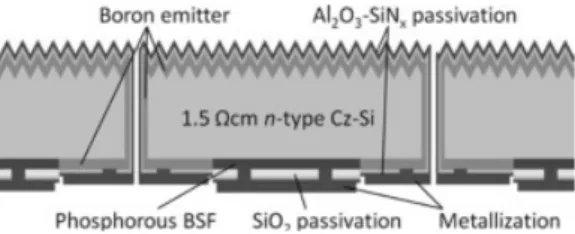
4.3.4 Al2O3 Aluminum oxide Al2O3 has recently emerged as a passivation layer for n-type c-Si solar cells owing to its excellent field-effect passivation that is associated with the

This cell exhibits higher JSC than the symmetric SiNW solar cells stemming from the increase in the light trapping path and the charge carrier generation in the radial junction due to

Triple-junction tandem solar cells with hydrogenated amorphous silicon (a-Si:H), hydrogenated amorphous silicon germanium (a-SiGe x :H), and hydrogenated nanocrystalline

The first investigation of the HJ silicon solar cells, in which an amorphous silicon emitter is deposited on a crystalline substrate, was reported by Fuhs et al. Then, in 1985,

First, a TiO 2 -based composite photoelectrode with Au NPs and luminescent ZrO 2 :Er 3+ phosphor NPs was used to improve the overall solar light harvesting through both the up- and

In regards to energy conversion efficiencies, for front- lit Si solar cells, the highest efficiency reported to date for an actual cell is 24.7 % by a method known as