1. Introduction
Thin film amorphous silicon-based solar cells are one of the most promising low-cost photovoltaic technologies. Hydrogenated amorphous silicon (a-Si:H) and hydrogenated nanocrystalline silicon (nc-Si:H) thin film are commonly used for application of multi-junction solar cells because they can be deposited on various substrates. These reasons have made the a-Si:H and µc-Si:H become potential candidates for device technology with low price. Research and development of a-Si:H based solar cell are now in a new stage aiming at mass production and cost reduction
1,2).
Radio frequency (RF) plasma enhanced chemical vapor deposition (PECVD) is one of the most popular industrial methods for the production. Although a uniform layer thickness is usually obtained under low deposition temperature, the films deposited by conventional 13.56 MHz RF PECVD method have low conductivity, low deposition rate, and high hydrogen content
2). To enhance the throughput of the PECVD process, a high deposition rate for thin films is required. The electrical and optical properties of thin films are known to be determined by its deposition conditions
2,3). The growth of high-quality thin films requires deposition conditions of high hydrogen dilution of silane (SiH
4), sufficiently high discharge power and deposition
temperature. An alternative deposition method is to use very high frequency (VHF) PECVD. The VHF PECVD offers the advantage of an enhanced gas dissociation rate, which results in the film deposition with a more stable phase. Additionally, during the VHF PECVD deposition, the self-bias, and therefore the ionic bombardment of the growing surface, are reduced as compared to the RF deposition, with a consequent reduction of structural damage and improvement of thin film quality
4).
The optical gap of a-Si:H is usually 1.72 eV whereas hydro- genated amorphous silicon oxide (a-SiO:H)
5-8)and carbide (a-SiC:H)
9-12)alloy, materials with carbon and oxygen bondings have optical gaps from 1.72 up to 1.87 eV. Hydrogenated amorphous silicon germanium (a-SiGe:H)
13)alloy which has bonding with germanium has a relatively lower optical gap.
For the a-SiO:H materials, the CO
2, H
2O, N
2O, O
2, etc. can be used as a source of oxygen, while CH
4, C
2H
2, etc. are found to be suitable for the a-SiC:H alloys. For the a-SiGe:H alloy, the GeH
4source gas is generally used. Materials with various optical gaps are very useful in designing multi-junction solar cells. The multi-junction solar cells have various absorption layers with different optical gaps and the full spectrum can be used. In particular, layers made using Oxygen are suitable for obtaining high efficiency because of their excellent electrical and optical properties.
Worldwide, tandem and triple junction solar cells have been actively studied, and the triple junction solar cells have the
DOI:https://doi.org/10.21218/CPR.2017.5.4.113 eISSN 2508-125X
Current Status of Thin Film Silicon Solar Cells for High Efficiency
Chonghoon Shin
1)․ Youn-Jung Lee
2)․ Jinjoo Park
1)․ Sunbo Kim
1)․ Hyeongsik Park
1)․ Sangho Kim
1)․ Junhee Jung
1)․ Junsin Yi
1,2)*
1)Department of Energy Science, Sungkyunkwan University, Suwon, 16419, Korea
2)School of Electronic Electrical Engineering, College of Information and Communication Engineering, Sungkyunkwan University, Suwon, 16419, Korea
Received July 31, 2017; Revised November 27, 2017; Accepted December 5, 2017
ABSTRACT: The researches on the silicon-based thin films are being actively carried out. The silicon-based thin films can be made as amorphous, microcrystalline and mixed phase and it is known that the optical bandgap can be controlled accordingly. They are suitable materials for the fabrication of single junction, tandem and triple junction solar cells. It can be used as a doping layer through the bonding of boron and phosphorus. The carbon and oxygen can bond with silicon to form a wide range of optical gap. Also, The optical gap of hydrogenated amorphous silicon germanium can be lower than that of silicon. By controlling the optical gaps, it is possible to fabricate multi-junction thin film silicon solar cells with high efficiencies which can be promising photovoltaic devices.
Key words: Amorphous silicon, Microcrystalline silicon, Intrinsic layer, Doping layer, Triple solar cells
*Corresponding author: [email protected]
ⓒ 2017 by Korea Photovoltaic Society
This is an Open Access article distributed under the terms of the Creative Commons Attribution Non-Commercial License (http://creativecommons.org/licenses/by-nc/3.0)
which permits unrestricted non-commercial use, distribution, and reproduction in any medium, provided the original work is properly cited.
113
world’s highest efficiency with a stabilized efficiency of 13.6%
14).
The amorphous material has high optical band gap but has low conductivities and it seems that the microcrystalline material is more promising to have higher efficiency. Especially, the doped materials are being investigated extensively. The p-type materials use diborane (B
2H
6)
15,16)and trimethyl boron (TMB) source gas
17)and the n-type use phosphine (PH
3) as source gasses
15). For the case of the p-type microcrystalline silicon, oxygen gas is used as a source to form p-type microcrystalline silicon oxide which has a high optical gap and high conductivity, and it is used as a window layer
18-24). Also, since its refractive index can be controlled, it can be used as an anti-reflective layer
25). By using the oxygen gas as a source the n-type micro- crystalline silicon can be made to be n-type microcrystalline silicon oxide. Since it has a low refractive index, it can be used as a back refractor layer
26-30)and it is used as an intermediate reflector for multi-junction solar cells
31-35).
2. Current status of developing of p-type layer (silicon oxide) for thin film silicon solar cells
Materials with wide optical gap should be used as a window layer for the single, tandem and triple junction solar cells. The reason is that light should penetrate the window layer. Thus, a wide optical gap which has low absorption is used. Since the window layer is in contact with TCO, the conductivity which affects the fill factor is important.
For contact layers, boron doped amorphous and materials with microcrystalline structure are used. To get a wide optical gap, silicon oxide or silicon carbide should be made within the film using CO
2or CH
4.
In this review, the focus will be on the silicon oxide. First, the
amorphous silicon is deposited by the plasma-enhanced chemical vapor deposition (PECVD) technique. SiH
4and H
2gasses are mostly used. For the doping gas, diborane (B
2H
6) and trimethyl boron (TMB, B(CH
3)
3) are used. The SiH
4is dissociated into SiH
3and H, H
2into H and H by electron and CO
2is dissociated into CO and O by hydrogen. As a result, silicon (Si) bonds with oxygen (O) forming silicon-oxygen (Si-O) alloy. In 1993, Watanabe et al. proposed the two-phase structure model of the Si-O alloy
35). The silicon-rich regions are surrounded by the oxygen-rich regions. The size of the silicon-rich regions and the relative contribution of the oxygen-rich regions depend on oxygen concentration. Various plasma parameters have been studied and they are applied to single, tandem and triple junction solar cells.
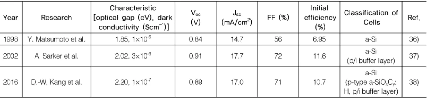
Table 1 shows the initial photovoltaic parameters of the best-achieved device performances and characteristics of p-type hydrogenated amorphous silicon oxide (p-type a-SiO
x:H) films.
The optical bandgap increases with oxygen to silane gas flow ratio, while the electrical conductivity decreases. The optical bandgap changes easily as a function of gas-source ratio from 1.3 to 2.0 eV. Hydrogenated amorphous silicon solar cells have been fabricated using p-type a-SiOx:H with around 1.85 eV optical band gap and a conductivity greater than 1×10
-7Scm
-1. The V
oc, J
scand conversion efficiency of the amorphous silicon solar cells are 0.84 V, 14.66 mA/cm
2and 6.95%, respectively
36).
Sometimes silicon carbide is used as a wide band gap material. The band gap of the silicon oxide and silicon carbide are similar. However, the p-type a-SiO:H films having thickness
≥ 10 nm has photoconductivity (σ
ph) one order of magnitude higher than that of p-type hydrogenated amorphous silicon carbide (p-type a-SiC:H) films. For 10 nm thick required for the window layer, the σ
phof p-type a-SiO:H film is ~10
2times higher than that of p-type a-SiC:H film. Single junction p-i-n structure a-Si solar cells are fabricated. The fill factor (FF) is 10% higher when fabricated with p-type a-SiO:H compared
Table 1. Initial photovoltaic parameters of best achieved device performances and characteristic film using p-type a-SiOx:H films in different device structures
Year Research Characteristic
[optical gap (eV), dark conductivity (Scm-1)]
Voc
(V) Jsc
(mA/cm2) FF (%) Initial efficiency
(%)
Classification of
Cells Ref.
1998 Y. Matsumoto et al. 1.85, 1×10⁻⁶ 0.84 14.7 56 6.95 a-Si 36)
2002 A. Sarker et al. 2.02, 3×10⁻⁶ 0.91 17.7 72 11.6 a-Si
(p/i buffer layer) 37)
2016 D.-W. Kang et al. 2.20, 1×10⁻⁷ 0.89 17.0 71 10.7
a-Si (p-type a-SiOxCy: H, p/i buffer layer)
38)
with p-type a-SiC:H. The efficiency is 11.6%, open-circuit voltage (V
oc) is 0.91 V and current density (J
sc) is 17.7 mA/cm
2 37).
p-type a-SiO
xC
y:H films are fabricated by adding Trim- ethylboron (TMB, B(CH
3)
3) doping gas to p-type a-SiO
x:H films. The band gap is between 2.14 to 2.20 eV without electrical conductivity deterioration. The response in short wavelength regions is increased improving J
scwhile maintaining FF and the efficiency improved from 10.4 to 10.7%
38).
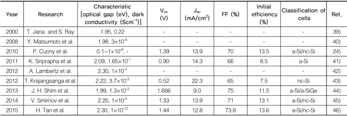
Table 2 shows the initial photovoltaic parameters of best-achieved device performances and characteristics of the film using p-type nanocrystalline silicon oxide (p-type nc-SiO
x:H) films. Although there are a number of ways to deposit nano- crystalline silicon (nc-Si:H) films, the material properties of the nano nc-Si:H thin films obtained using different deposition methods are close to each other. There have been two mecha- nisms of p-type nc-Si:H thin films. The two mechanisms of deposition of plasma from SiH
4gas are surface diffusion,
58,59)and selective etching
60-62). Both have been proposed to explain the deposition of nc-Si:H thin films. The surface diffusion was considered to improve the mobility of the deposition precursors, by the many hydrogen atoms that impinge on the surface. For selective etching, amorphous and crystalline phases are assumed to be deposited simultaneously; atomic hydrogen impinges on the film surface, and the amorphous material is selectively etched, leaving behind a crystal film. The chemical approach states that hydrogen atoms annihilate the strained Si-Si bonds in a-Si:H, and promote the crystallization
63-66). The concentration of hydrogen in silicon network, and within the film, is dependent on the chemical potential of the hydrogen in the plasma state.
When the hydrogen chemical potential is low, the weak Si-Si bonds break while the strong bonds remain. The concentration of hydrogen increases with the chemical potential, but the
hydrogen concentration within the a-Si:H films decreases, while the hydrogen is being added to plasma
67). Reconstruction of the silicon network occurs by replacing the weak bonds by strong ones when the chemical potential reaches a certain level.
Some structural defects, which have not been reconstructed, remain at the interface of amorphous and crystalline regions.
The insertion of hydrogen to the Si-Si bond causes the formation of a Si-H-Si configuration
68,69). The structure, which is in the transition amorphous-to-crystalline, gets mediated by relaxation of the strained Si-Si bonds. The hydrogen atoms that left the bond-centered location break or relax the strained Si-Si bonds.
Next, local structural rearrangements yield c-Si like bond lengths and angles
70). The CO
2/SiH
4gas ratio is the main process condition influencing the proportion of oxygen in nc-SiO
x:H films. When H
2/SiH
4the gas ratio is increased, the hydrogen atoms cause the CO
2gas to break into C-O and O-O bonds. This results in the silicon-oxygen (Si-O) bonds in nc-SiO
x:H. The p-type nc-SiO
x:H is fabricated with the B
2H
6source gas.
There are several critical requirements for a promising p-doped material as window layer: (1) good ohmic contact with front TCO layer; (2) high band gap to achieve high build-in voltage (V
bi) and thus high open-circuit voltage (V
oc); (3) good conductivity to obtain high fill factor (FF); and (4) low absorption loss over the short wavelengths range (300 –600 nm)
46). The materials that have these four advantages are p-type nc-SiO
x:H films. In addition, the function as a nucleation layer for nanocrystalline silicon growth might be desired. (1) The electrical conductivity depends strongly on the crystalline volume fraction and (2) the band gap depends strongly on the oxygen content. The introduction of oxygen suppresses the nucleation of Si nanocrystallites. Therefore, p-type nc-SiO
x:H film with low oxygen content should be used for the contact
Table 2. Initial photovoltaic parameters of best achieved device performances and characteristic film using p-type nc-SiOx:H films in different device structures
Year Research Characteristic
[optical gap (eV), dark conductivity (Scm-1)]
Voc
(V) Jsc
(mA/cm2) FF (%) Initial efficiency
(%)
Classification of
cells Ref.
2000 T. Jana and S. Ray 1.95, 0.22 - - - 39)
2008 Y. Matsumoto et al. 1.98, 3×10⁻⁴ - - - 40)
2010 P. Cuony et al. 0.1~1×10⁻⁹, - 1.39 13.9 70 13.5 a-Si/nc-Si 24)
2011 K. Sriprapha et al. 2.09, 1.65×10⁻¹ 0.90 14.3 66 8.5 a-Si 41)
2012 A. Lambertz et al. 2.30, 1×10⁻² - - - 42)
2012 T. Krajangsanga et al. 2.22, 3.7×10⁻³ 0.52 22.3 65 7.5 nc-Si 43)
2013 J. H. Shim et al. 1.99, 1.3×10⁻³ 1.686 9.0 75 11.5 a-Si/a-SiGe 44)
2014 V. Smirnov et al. 2.25, 1×10⁻³ 1.33 13.9 71 13.1 a-Si/nc-Si 45)
2015 H. Tan et al. 2.30, 1×10-12 1.44 12.8 73.8 13.6 a-Si/nc-Si 46)
layer, to guarantee growth of highly conductive Si nano- crystallites in the initial few nanometers. With p-type nc-SiO
x:H as p-layer, the optimal p-type nc-SiO
x:H film has high oxygen content and thus high band gap, resulting in higher V
ocand better spectral response than the standard p-type amorphous silicon carbide alloys (p-SiC) based window layer. Although the optimal p-type nc-SiO
x:H film has very low planar conductivity (in the order of 10
–12S/cm), the filament-like Si nanocrystallites which grow perpendicular to the substrate enable the adequate transverse conduction for the solar cells. Consequently, a-Si:H solar cells with V
oc> 1 V and FF > 70% have been obtained.
Finally, the p-type nc-SiO
x:H window layers were successfully applied to thin-film silicon multi-junction solar cells. A higher initial efficiency has been achieved in a-Si:H/nc-Si:H tandem solar cells
24,39,42-46).
3. Current status of developing of i-type layer (silicon oxide) for thin film silicon solar cells
A multi-junction structure is essential for high-efficiency silicon-based thin-film solar cells owing to the efficient use of the solar spectrum. Triple-junction tandem solar cells with hydrogenated amorphous silicon (a-Si:H), hydrogenated amorphous silicon germanium (a-SiGe
x:H), and hydrogenated nanocrystalline silicon (nc-Si:H) absorber layers have been intensively studied and an efficiency of 16.3% has been achieved so far
71). The band gap of the top, middle, and bottom cells are 1.8, 1.45, and 1.1 eV, respectively. However, the theoretical analysis performed by Yunaz et al.
72)suggests that increasing the band gap of the top cell up to 2.0 eV increases efficiency owing to the increase in V
oc. Therefore, new wide band gap amorphous silicon-based materials should be developed for the top cell.
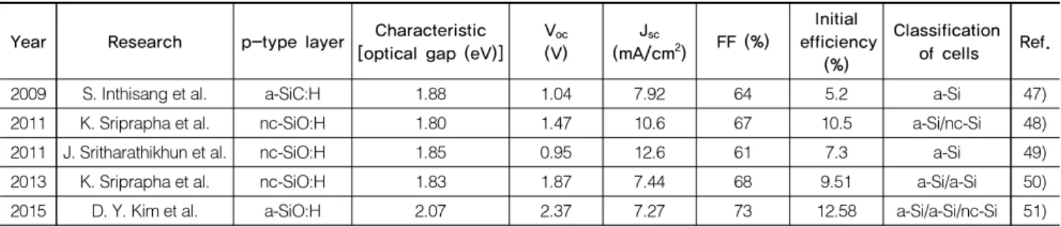
Table 3 shows initial photovoltaic parameters of best achieved device performances and characteristic film using i-type a-SiOx:H films in different device structures. The effect of H
2on the intrinsic a-SiO
x:H (i-type a-SiO
x:H) films has been investigated using the mixture of SiH
4, H
2, and CO
2.H
2dilution strongly affected the electrical and optical properties as well as structural properties. Photo and dark conductivity measurements revealed that the photosensitivity of the films increased with increasing H
2dilution until the phase transition from the amorphous phase to the microcrystalline phase. a-SiO
x:H solar cells fabricated in the phase transition region showed a high V
ocof 1.04 V. This high V
ocin the phase transition region is attributed to the high photosensitivity of the a-Si
1-xO
x:H films.
The solar cells also showed a slightly higher light-induced degradation ratio than with standard a-Si:H solar cells
47). The temperature coefficient (TC) of solar cells indicated that the values of TC for conversion efficiency (η) of the double- junction solar cells were inversely proportional to the initial V
oc, which corresponds to the band gap of the top cells. The TC for η of typical a-SiO:H/nc-Si:H was -0.32%/°C, lower than the value of conventional a-Si:H/nc-Si:H solar cell. Both the a-SiO:H/nc-Si:H solar cell and the conventional solar cell showed the same light induced degradation ratio of about 20%
48). The effect of plasma power density on the defect density of the i-type a-SiO
x:H films has been investigated. The defect density is a critical parameter for estimating the thin film silicon- based quality. The defect density was increased with increasing plasma power density. Plasma power density strongly affected i-type a-SiO:H film properties. The best a-SiO:H based solar cell showed a conversion efficiency of 7.3% (V
oc= 0.95 V, J
sc= 12.6 mA/cm
2, and FF = 0.61). The superior of the spectral response in short wavelength showed the potential of i-type a-SiO:H layer for the use as an absorber layer in a top cell of multi-junction solar cells
49). For a-SiO:H/a-Si:H double-junction solar cells, studies are carried out about a high V
oc, a low TC for
Table 3. Initial photovoltaic parameters of best achieved device performances and characteristic film using i-type a-SiOx:H films in different device structures
Year Research p-type layer Characteristic
[optical gap (eV)] Voc
(V) Jsc
(mA/cm2) FF (%) Initial efficiency
(%)
Classification of cells Ref.
2009 S. Inthisang et al. a-SiC:H 1.88 1.04 7.92 64 5.2 a-Si 47)
2011 K. Sriprapha et al. nc-SiO:H 1.80 1.47 10.6 67 10.5 a-Si/nc-Si 48)
2011 J. Sritharathikhun et al. nc-SiO:H 1.85 0.95 12.6 61 7.3 a-Si 49)
2013 K. Sriprapha et al. nc-SiO:H 1.83 1.87 7.44 68 9.51 a-Si/a-Si 50)
2015 D. Y. Kim et al. a-SiO:H 2.07 2.37 7.27 73 12.58 a-Si/a-Si/nc-Si 51)
η as well as a low degradation ratio. The trade-off between the band gap and the photo gain of the i-type a-SiO:H films. The highest initial η of 10.2% with a high V
ocof 1.88 V was obtained from the a-SiO:H/a-Si:H double-junction solar cell, compared to the conventional a-Si:H/a-Si:H solar cell. The a-SiO:H/
a-Si:H solar cell exhibits a higher η, better temperature dependent behavior, and a lower degradation ratio. These advantages are due to the enhancement of the V
oc, which is caused by using the wide band gap a-SiO:H films. These results have verified that i-type a-SiO:H films have a great potential for use as absorption layers of the top cell of multi-junction silicon-based thin-film solar cells, which are more attractive for operating in a high- temperature environment or a tropical climate. The a-SiO:H based solar cells with low TC together with low degradation rate are attractive for use in a high-temperature environment or a tropical climate
50).
4. Current status of developing of n-type layer (silicon oxide) for thin film silicon solar cells
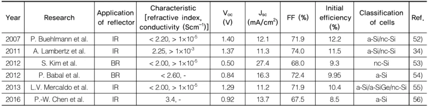
A multi-junction solar cell consists of a high-gap a-Si:H top cell and a low-gap μc-Si:H bottom cell stacked on top of each other. The thickness of the a-Si:H cell should be as thin as possible to minimize the impact of light-induced degradation and thus, its current generally limits the current of the multi- junction device. To overcome this issue, an intermediate reflecting layer (IRL) can be introduced between the two cells to increase the current of the top cell. The refractive index (n) of the intermediate layer which acts as a reflector should be lower than that of silicon. The layer which serves as IRL is required to be sufficiently conductive to avoid blocking current and as transparent as possible to minimize the current losses due to
absorption of light outside the active layers
52). Table 4 shows initial photovoltaic parameters of best achieved device performances and characteristic film using n-type nc-SiOx:H films in different device structures. (Intermediate reflector : IR, back reflector : BR). The n-type nc-SiO
x:H which is based on the silicon oxide has optical and electrical properties suitable to serve as intermediate reflectors. Using the n-type nc-SiO
x:H film, initial micromorph cell efficiency of 12.2% (V
oc=1.40 V, FF=71.9%, and J
sc=12.1 mA/cm
2) is obtained
52).
By increasing the oxygen content, it is possible to get a high band gap and low n but the electrical property is insufficient. To improve the property, CO
2and H
2have been investigated.
Tuning the trade-off between a highly conductive μc-Si:H fraction and an a-SiO
x:H phase with high oxygen content (O) yields a material with a combination of low refractive index and high band gap at sufficient conductivity (E
04=2.4 eV, n=2.1 at σ=10
-5S/cm). Using this IRL, a-Si:H/μc-Si:H tandem solar cells are fabricated and an efficiency of 11.5% is achieved
34).
To improve the light management of silicon thin-film solar cells, the n-type nc-SiOx:H films are used as IRL. The effects of O on optical, electrical and structural properties of n-type nc-SiO
x:H films have been investigated. With increasing O in n-type nc -SiO
x:H film, the optical band gap is widened due to the increased amount of Si-O bonds, while the conductivity decreases accordingly. A similar trend is found in the case of bi-phase n-type nc-SiOx:H comprising wide-band gap a-SiO
x:H phase and conductive μc-Si:H phase. For a-Si:H/a-Si
1-xGe
x:H tandem cell, employing n-type μc-SiO
x:H as IRL increases the current density of the top cell. The a-Si:H/a-Si
1-xGe
x:H tandem cell with efficiency of 9.2%, V
oc= 1.58 V, J
sc= 8.43 mA/cm
2, and FF = 68.4% is obtained
56).
To achieve more efficient light trapping and higher current density for nc-Si:H solar cells, the parasitic absorption losses occurring at the back and front electrodes should be minimized
Table 4. Initial photovoltaic parameters of best achieved device performances and characteristic film using n-type nc-SiOx:H films in different device structures. (Intermediate reflector : IR, back reflector : BR)
Year Research Application
of reflector
Characteristic [refractive index, conductivity (Scm-1)]
Voc
(V) Jsc
(mA/cm2) FF (%) Initial efficiency
(%)
Classification of cells Ref.
2007 P. Buehlmann et al. IR < 2.20, > 1×10⁻⁵ 1.40 12.1 71.9 12.2 a-Si/nc-Si 52)
2011 A. Lambertz et al. IR 2.25, > 1×10⁻³ 1.37 11.3 74.0 11.5 a-Si/nc-Si 34)
2012 S. Kim et al. BR < 2.00, > 1×10⁻⁵ 0.50 27.4 68.0 9.3 nc-Si 53)
2012 P. Babal et al. BR < 2.60, - 0.84 16.3 72.4 9.95 a-Si 54)
2013 L.V. Mercaldo et al. IR < 2.00, > 1×10⁻⁵ 1.29 11.2 71.9 10.4 a-Si/a-SiGe/nc-Si 55)
2016 P.-W. Chen et al. IR 3.4, - 0.92 13.7 67.5 8.5 a-Si 56)
by optimizing the back reflector configuration and/or the front electrode material such as TCO.
To improve the reflection performance of the back reflector (BR), the refractive index of the BR material should be minimized for total reflection. The promising material satisfying this condition is an n-type nc-SiO
xfilm which is composed of amorphous SiO
xand conductive n-type microcrystalline Si. The n-type nc-SiO
xfilm with high reflectivity and high transparency is a novel BR material. The n-type nc-SiO
xfilms have a lower refractive index and lower absorption spectra at long wavelengths of >700 nm compared to the conventional ZnO:Al back reflector materials. The n-type nc-SiO
xlayer was applied as a back reflector for μc-Si:H solar cells, boosting not only the J
scbut also the V
ocand the FF. This result suggests that the anisotropic characteristics of the microstructure and the electrical conductivity of the n-type nc-SiO
xlayer may reduce the shunt current at the back contacts of thin-film Si solar cells
53,54).
5. Current status of high-efficiency thin film solar cell
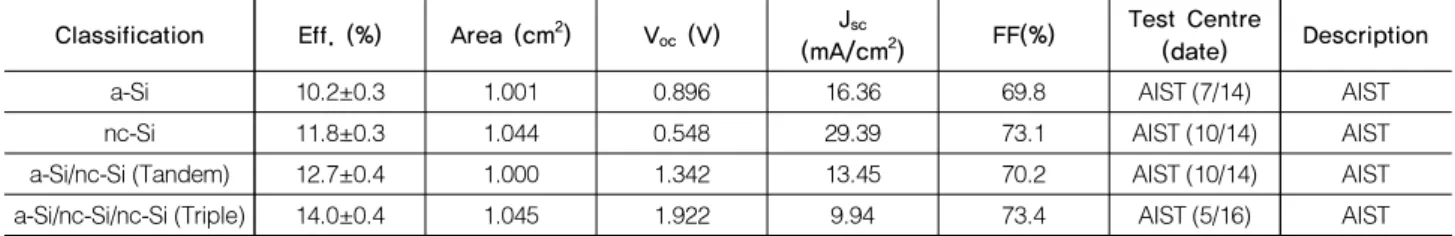
Table 5 shows the present status of the conversion efficiency of thin film silicon solar cells. The quality of undoped a-Si:H layers deposited either by triode or diode PECVD is high and a p–i–n device in a superstrate configuration is fabricated at AIST.
As a front TCO substrate, a commercially available SnO
2- coated glass (Asahi-VU) was used. For the p-layer, a very thin a-SiC:H is used. An a-Si:H p–i buffer layer is effective in reducing light-induced degradation while keeping V
ocreasonably high. The optimized a-Si:H single-junction solar cells have stabilized efficiency of 10.1-10.2% and for a-Si:H/ μc-Si:H tandem solar cells, the stabilized efficiency of 12.69% is obtained
73).
Substrate-type n-i-p nc-Si:H cells are fabricated using honeycomb textures at AIST. The structure of the solar cell consists of honeycomb-textured substrate/Ag/ZnO/nc-Si:H n-i-p
layers/In
2O
3:Sn (ITO, 70 nm)/Ag grid.
To reduce the absorption loss, wide-gap nanocrystalline silicon oxides (nc-SiO
x:H) are used for the n-type and p-type nc-Si:H. When the textures had moderate aspect ratios, we could find the optimum period to get high J
sc. Based on these findings, we have fabricated optimized μc-Si:H cells achieving a high efficiency exceeding 10% and a J
scof 30 mA/cm
2 74).
Using the honeycomb textures mentioned above, a-Si:H/nc- Si:H/nc-Si:H triple-junction cells are fabricated at AIST. In a single-junction μc-Si:H cell with IOH front contact, a high J
scof approximately 33 mA/cm
2is achieved. For the case of multi-junction cells, the growth of μc-Si:H layers is interrupted by doped layers or intermediate reflectors, such as nc-SiO
x:H film. The investigation on the film stacks of nc-Si:H/nc-SiO
x:H layers has been carried out. These technologies were also combined into a-Si:H/nc-Si:H/nc-Si:H triple-junction cells and a world record stabilized efficiency of 13.6% was achieved
75).
6. Conclusions
The phase of silicon-based thin films can be controlled variously and the electrical and optical properties can be optimized by plasma parameters for application to photovoltaic devices. To get high efficiency, new materials are needed. One of the promising materials is the silicon oxide (SiO
x). The technologies on fabricating a-SiO
x:H phase with wide bad gap, μc-Si:H phase with high conductivity and nc-SiO
x:H with bi-phase have been studied. Using these technologies, it has been possible to obtain a wold record stabilized efficiency.
Acknowledgments
This work was supported by the New & Renewable Energy Core Technology Program of the Korea Institute of Energy Technology Evaluation and Planning (KETEP), granted financial resource from the Ministry of Trade, Industry & Energy, Republic of Korea (No. 20143030011960).
Table 5. Present status of conversion efficiency of thin film silicon solar cells [57]
Classification Eff. (%) Area (cm2) Voc (V) Jsc
(mA/cm2) FF(%) Test Centre
(date) Description
a-Si 10.2±0.3 1.001 0.896 16.36 69.8 AIST (7/14) AIST
nc-Si 11.8±0.3 1.044 0.548 29.39 73.1 AIST (10/14) AIST
a-Si/nc-Si (Tandem) 12.7±0.4 1.000 1.342 13.45 70.2 AIST (10/14) AIST
a-Si/nc-Si/nc-Si (Triple) 14.0±0.4 1.045 1.922 9.94 73.4 AIST (5/16) AIST
References
1. Y. Ide, Y. Saito, A. Yamada, M. Konagai, “Intrinsic Micro- crystalline Silicon Thin Films Prepared by Hot-Wire Cell Method and Their Application to Solar Cells”, Jpn. J. Appl.
Phys. Vol. 42, pp. 1521, 2003.
2. M. Isomura, M. Kondo, A. Matsuda, “Device Grade Amorphous Silicon Prepared by High-Pressure Plasma”, Jpn. J. Appl. Phys.
Vol. 41, pp. 1947-1951, 2002.
3. S. M. Iftiquar, “The roles of deposition pressure and rf power in opto-electronic properties of a-SiO:H films”, J. Phys. D: Appl.
Phys. Vol. 31, pp. 1630-1641, 1998.
4. C. Shin, S.M. Iftiquar, J. Park, Y. Kim, S. Baek, J. Jang, M Kim, J. Jung, Y. Lee, S. Kim, J. Yi, “Optimization of intrinsic hydrogenated amorphous silicon deposited by very high-fre- quency plasma-enhanced chemical vapor deposition using the relationship between Urbach energy and silane depletion frac- tion for solar cell application”, Thin Solid Films Vol. 547, pp.
256-262, 2013.
5. S. M. Iftiquar, “The roles of deposition pressure and rf power in opto-electronic properties of a-SiO:H films”, J. Phys. D: Appl.
Phys. Vol. 31, pp. 1630-1641, 1998.
6. W. Beyer, “Infrared absorption and hydrogen e€usion of hy- drogenated amorphous silicon-oxide films”, J. Non-Cryst.
Solids, Vol. 266-269, pp. 845-8497, 2000.
7. S. Mukhopadhyay, S. Ray, “Silicon rich silicon oxide films de- posited by radio requency plasma enhanced chemical vapor deposition method: Optical and structural properties”, Appl.
Surf. Sci., Vol. 257, pp. 9717– 9723, 2011.
8. J. Sritharathikhun, A. Moollakorn, S. Kittisontirak, A. Limmanee, K. Sriprapha, “High quality hydrogenated amorphous silicon oxide film and its application in thin film silicon solar cells”, Current Applied Physics Vol. 11, pp. S17-S20, 2011.
9. S.M. Iftiquar, A.K. Barua, “Control of the properties of wide- bandgap a-SiC : H films prepared by RF PECVD method by varying methane flow rate”, Solar Energy Materials and Solar Cells Vol. 56, pp. 117-123, 1999.
10. C.-H. Cheng, Y.-H. Lin, J.-H. Chang, C.-I. Wu, G.-R. Lin,
“Semi-transparent Si-rich SixC1-x p–i–n photovoltaic solar cell grown by hydrogen-free PECVD”, RSC Adv., Vol. 4, pp.
18397-18405, 2014.
11. B. Yan, L. Zhao, B. Zhao, J. Chen, H. Diao, G. Wang, Y. Mao, W. Wang, “Wide bandgap p-type window layer prepared by tri- methylboron doping at high temperature for a-Si:H superstrate solar cell”, J. Non-Cryst. Solids, Vol. 385, pp. 3243-3247, 2012.
12. S. Y Myong, K. S. Lim and J. M. Pears, “Double amorphous silicon-carbide p-layer structures producing highly stabilized pin-type protocrystalline silicon multilayer solar cells”, Appl.
Phys. Lett., Vol. 87, pp.193509-1-193509-3, 2005.
13. P. Chaudhuri, A.R. Middya and S. Ray, “Photogeneration and recombination of carriers in hydrogenated amorphous silicon germanium alloys”, Solar Energy Materials and Solar Cells,
Vol. 30, pp. 233-243, 1993.
14. Sai H, Matsui T, Koida T, Matsubara K, Kondo M, Sugiyama S, Katayama H, Takeuchi Y, Yoshida I., “Triple-junction thin- film silicon solar cell fabricated on periodically textured sub- strate with a stabilized efficiency of 13.6%”, Appl. Phys. Lett., Vol 106, pp. 213902-1-21390-4, 2015.
15. W. Spear and P. L. Comber, “Substitutional doping of amor- phous silicon”, Solid State Comm. Vol. 17 pp. 1193-1196, 1975.
16. K. Yoon, Y. Kim, J. Park, C. H. Shin, S. Baek, J. Jang, S. M.
Iftiquar, J. Yi, “Preparation and characterization of p-type hy- drogenated amorphous silicon oxide film and its application to solar cell”, J. of Non-Cryst. Solids Vol. 357, pp. 2826-2832, 2011.
17. B. Yan, L. Zhao, B. Zhao, J. Chen, H. Diao, G. Wang, Y. Mao, W. Wang, “Wide bandgap p-type window layer prepared by tri- methylboron doping at high temperature for a-Si:H superstrate solar cell”, J. Non-Cryst. Solids, Vol. 358, pp. 3243-3247, 2012.
18. H. Tan, P. Babal, M. Zeman, A. H. M.Smets, “Wide band gap p-type nanocrystalline silicon oxide as window layer for high performance thin-film silicon multi-junction solar cells”, Sol.
Energ. Mat. Sol. Cells, Vol. 132, pp. 597-605, 2015.
19. V. Smirnov, A. Lambertz, S. Tillmanns, and F. Finger, “p- and n-type microcrystalline silicon oxide (μc-SiOx:H) for applica- tions in thin film silicon tandem solar cells”, Can. J. Phys., Vol.
92, pp. 932-935, 2014.
20. J. H. Shim, S.-W. Ahn, H.-M, Lee, “Microcrystalline silicon oxide (mc-SiO:H) alloys as a contact layer for highly efficient Si thin film solar cell”, Curr. Appl. Phys., Vol. 13, pp. 1401-1403, 2013.
21. T. Krajangsang, S. Kasashima, A. Hongsingthong, P. Sichanugrist, M. Konagai, “Effect of p-μc-Si1-xOx:H layer on performance of hetero-junction microcrystalline silicon solar cells under light concentration”, Curr. Appl. Phys., Vol. 12, pp. 515-520, 2012.
22. A. Lambertz, F. Finger, B. Hollander, J. K. Rath, R. E. I.
Schropp, “Boron-doped hydrogenated microcrystalline silicon oxide (μc-SiOx:H) for application in thin-film silicon solar cells”, J. Non-Cryst. Solids, Vol. 358, pp. 1962-1965, 2012.
23. K. Sriprapha, N. Sitthiphol, P. Sangkhawong, V. Sangsuwan, A. Limmanee, J. Sritharathikhun. “p-Type hydrogenated sili- con oxide thin film deposited near amorphous to microcrystal- line phase transition and its application to solar cells”, Curr.
Appl. Phys., Vol. 11, pp. 547-549, 2011.
24. P. Cuony, M. Marending, T. L. Alexander, M. Boccard, G.
Bugnon, M. Despeisse, C. Ballif, “Mixed-phase p-type silicon oxide containing silicon nanocrystals and its role in thin-film silicon solar cells”, Appl. Phys. Lett., Vol, 97, pp. 213502, 2010.
25. K. Schwanitz, S. Klein,T. Stolley, M. Rohde,D. Severin, R.
Trassl, “Anti-reflective microcrystalline silicon oxide p-layer for thin-film silicon solar cells on ZnO”, Sol. Energ. Mat. Sol.
Cells, Vo. 105, pp. 187-191, 2012.
26. V. Smirnov, A. Lambertz, F. Finger, “Electronic and structural properties of n-type microcrystalline silicon oxide (μc-SiOx:H)
films for applications in thin film silicon solar cells”, Energy Procedia, Vol. 84, pp. 71-77, 2015.
27. S. Y. Myong, L. S. Jeon, “Improved light trapping in thin-film silicon solar cells via alternated n-type silicon oxide reflectors”, Sol. Energ. Mat. Sol. Cells, Vo. 119, pp. 77-83, 2013.
28. C. Banerjee, T. Srikanth, U. Basavaraju, R. M. Tomy, M. G.
Sreenivasan, K. Mohanchandran, S. Mukhopadhyay, A. K.
Barua, “Development of n-µc-SiOx:H as cost effective back re- flector and its application to thin film amorphous silicon solar cells”, Sol. Energy, Vol. 97, pp. 591-595, 2013.
29. S. Kim, H. Lee, J.-W. Chung, S.-W. Ahn, H.-M. Lee, “n-Type microcrystalline silicon oxide layer and its application to high-performance back reflectors in thin-film silicon solar cells”, Curr. Appl. Phys., Vol. 13, pp. 743-747, 2013.
30. X. D. Zhang, Q. Yue, X. X. Zheng, X. H. Geng, Y. Zhao,
“Plasma deposition of n-SiOx nanocrystalline thin film for en- hancing the performance of silicon thin film solar cells”, Thin Solid Films, Vol. 520, pp. 684-688, 2011.
31. P.-W. Chen, P.-L. Chen, C.-C. Tsai, “Development of Wider Bandgap n-type a-SiOx:H and μc-SiOx:H as Both Doped and Intermediate Reflecting Layer for a-Si:H/a-Si1-xGex:H Tandem Solar Cells”, Electron. Mater. Lett., Vol. 12, pp. 445-450, No. 4, 2016.
32. V. Smirnov, A. Lambertz, B. Grootoonk, R. Carius, F. Finger,
“Microcrystalline silicon oxide (μc-SiOx:H) alloys: A versatile material for application in thin film silicon single and tandem junction solar cells”, J. Non-Cryst. Solids, Vol. 358, pp.
1954-1957, 2012.
33. S. Kirner, S. Calnan, O. Gabriel, S. Neubert, M. Zelt, B.
Stannowski, B. Rech, R. Schlatmann, “An improved sili- con-oxide-based intermediate-reflector for micromorph solar cells”, Phys. Status Solidi C, Vol. 9, No. 10-11, pp. 2145-2148, 2012.
34. A. Lambertz, T. Grundler, F. Finger, “Hydrogenated amor- phous silicon oxide containing a microcrystalline silicon phase and usage as an intermediate reflector in thin-film silicon solar cells”, J. Appl. Phys., Vol. 109, pp. 113109, 2011.
35. H. Watanabe, K. Haga, T. Lohner, “Structure of high-photo- sensitivity silicon-oxygen alloy films”, J. Non-Cryst. Solids, Vol. 164-166, pp. 1085-1088, 1993.
36. Y. Matsumoto, F. Meléndez, R. Asomoza, “Plasma CVD de- posited p-type silicon oxide wide-bandgap material for solar cells”, Sol. Energy. Mat. Sol. Cells, Vo. 52, pp. 251-260, 1998.
37. A. Sarker, A. K. Barua, “Development of High Quality P-Type Hydrogenated Amorphous Silicon Oxide Film and Its Use in Improving the Performance of Single Junction Amorphous Silicon Solar Cells”, Jpn. J. Appl. Phys., Vol. 41, pp. 765-769, 2002
38. D.-W. Kang, P. Sichanugrist, B. Janthong, M. A. Khan, C.
Niikura, M. Konagai, “Development of Wide Band Gap P-a-SiOxCy:H Using Additional Trimethylboron as Carbon Source Gas”, Electron. Mater. Lett., Vol. 12, No. 4, pp.
462-467, 2016.
39. T. Jana, S. Ray, “Microcrystalline silicon phase in silicon oxide thin films developed by photo-CVD technique”, Thin Solid Films Vol. 376, pp. 241-248, 2000.
40. Y. Matsumoto, Z. Yu, R. V. Sánchez, “Microcrystalline-phase p-type a-Si:O:H windows prepared by Cat-CVD”, Sol. Energy.
Mat. Sol. Cells, Vol. 92, pp. 576-580, 2008.
41. K. Sriprapha, N. Sitthiphol, P. Sangkhawong, V. Sangsuwan, A. Limmanee, J. Sritharathikhun, “p-Type hydrogenated sili- con oxide thin film deposited near amorphous to microcrystal- line phase transition and its application to solar cells”, Curr.
Appl. Phys., Vol. 11, pp. S47-S49, 2011.
42. A. Lambertz, F. Finger, B. Hollander, J. K. Rath, R. E. I.
Schropp, “Boron-doped hydrogenated microcrystalline silicon oxide (μc-SiOx:H) for application in thin-film silicon solar cells”, J. Non-Cryst. Solids, Vol. 358, pp. 1962-1965, 2012.
43. T. Krajangsanga, S. Kasashimaa, A. Hongsingthonga, P.
Sichanugrista, M. Konagai, “Effect of p-μc-Si1xOx:H layer on performance of hetero-junction microcrystalline silicon solar cells under light concentration”, Curr. Appl. Phys., Vol. 12, pp.
515-520, 2012.
44. J. H. Shim, S.-W. Ahn, H.-M. Lee, “Microcrystalline silicon oxide (μc-SiO:H) alloys as a contact layer for highly efficient Si thin film solar cell”, Curr. Appl. Phys., Vol. 13, pp. 1401-1403, 2013.
45. V. Smirnov, A. Lambertz, S. Tillmanns, and F. Finger, “p- and n-type microcrystalline silicon oxide (μc-SiOx:H) for applica- tions in thin film silicon tandem solar cells:, Can. J. Phys., Vol.
92, pp. 932-935, 2014.
46. H. Tan, P. Babal, M. Zeman, A. H. M.Smets, Wide band gap p-type nanocrystalline silicon oxide as window layer for high performance thin-film silicon multi-junction solar cells”, Sol.
Energy. Mat. Sol. Cells, Vol. 132, pp. 597-605, 2015.
47. S. Inthisang, K. Sriprapha, S. Miyajima, A. Yamada, M.
Konagai, “Hydrogenated Amorphous Silicon Oxide Solar Cells Fabricated near the Phase Transition between Amorphous and Microcrystalline Structures”, Jpn. J. Appl. Phys., Vol. 48, pp.
122402, 2009.
48. K. Sriprapha, C. Piromjit, A. Limmanee, J. Sritharathikhun,
“Development of thin film amorphous silicon oxide/micro- crystalline silicon double-junction solar cells and their temper- ature dependence”, Sol. Energy. Mat. Sol. Cells, Vol. 95, pp.
115-118, 2011.
49. J. Sritharathikhun, A. Moollakorn, S. Kittisontirak, A. Limmanee, Kobsak Sriprapha, “High quality hydrogenated amorphous sil- icon oxide film and its application in thin film silicon solar cells”, Curr. Appl. Phys., Vol. 11, pp. S17-S20, 2011.
50. K. Sriprapha, A. Hongsingthong, T. Krajangsang, S. Inthisang, S. Jaroensathainchok, A. Limmanee, W. Titiroongruang, J.
Sritharathikhun, “Development of thin film a-SiO:H/a-Si:H double-junction solar cells and their temperature dependence”, Thin Solid Films, Vol. 546, pp. 398-403, 2013.
51. D. Y. Kim, E. Guijt, F. T. Si, R. Santbergen, J. Holovský, O.
Isabella, R. A.C.M.M. van Swaaij, M. Zeman, “Fabrication of
double- and triple-junction solar cells with hydrogenated amor- phous silicon oxide (a-SiOx:H) top cell ”, Sol. Energy. Mat. Sol.
Cells, Vo. 141, pp. 148-153, 2015.
52. P. Buehlmann, J. Bailat, D. Dominé, A. Billet, F. Meillaud, A.
Feltrin, C. Ballif, “In situ silicon oxide based intermediate re- flector for thin-film silicon micromorph solar cells”, Appl.
Phys. Lett., Vol, 91, pp. 1-3, 2007.
53. S. Kim, H. Lee, J.-W. Chung, S.-W. Ahn, H.-M. Lee, “n-Type microcrystalline silicon oxide layer and its application to high-performance back reflectors in thin-film silicon solar cells”, Curr. Appl. Phys., Vol. 13, pp. 743-747, 2013.
54. P. Babal, J. Blanker, R. Vasudevan, A. H. M. Smets, M.
Zeman, “Microstructure analysis of n-doped μc-SiOx:H re- flector layers and their implementation in stable a-Si:H p-i-n junctions”, Proc. 38th IEEE Photovoltaic Specialists Conf., pp.
321-326, 2012.
55. L. V. Mercaldo, P. D. Veneri, I.Usatii, E. M. Esposito, G.
Nicotra, “Properties of mixed phase n-doped silicon oxide lay- ers and application in micromorph solar cells”, Sol. Energy.
Mat. Sol. Cells, Vo. 119, pp. 67-72, 2013.
56. P.-W. Chen, P.-L. Chen, C.-C. Tsai, “Development of Wider Bandgap n-type a-SiOx:H and μc-SiOx:H as Both Doped and Intermediate Reflecting Layer for a-Si:H/a-Si1-xGex:H Tandem Solar Cells”, Electron. Mater. Lett., Vol. 12, pp. 445-450, 2016.
57. M. A. Green, K. Emery, Y. Hishikawa, W. Warta, E. D. Dunlop, D. H. Levi, A. W. Y. Ho-Baillie, “Solar cell efficiency tables (version 49)”, Prog. Photovolt: Res. Appl., Vol. 25, pp. 3-13, 2017.
58. K. Nomoto, Y. Urano, J. Guizot, L. Ganguly, A. Matsuda,
“Role of Hydrogen Atoms in the Formation Process of Hydrogenated Microcrystalline Silicon”, Jpn. J. Appl. Phys Vol. 29, pp. 1372-1375, 1990.
59. M. Katiyar, J. R. Abelson, “Investigation of hydrogen plasma induced phase transition from a-Si:H to mc-Si:H using real time infrared spectroscopy”, Mater. Sci. Eng., A Vol. 304-306, pp.
349-352, 2001.
60. N. Layadi, C. Roca, B. Drévillon, I. Solomon, “Real-time spec- troscopic ellipsometry study of the growth of amorphous and microcrystalline silicon thin films prepared by alternating sili- con deposition and hydrogen plasma treatment”, Phys. Rev. B, Condens. Matter Vol. 52, pp. 5136-5143, 1995.
61. M. Fontcuberta, A. Bertomeu, C. Roca, “The role of hydrogen in the formation of microcrystalline silicon”, Mater. Sci. Eng., B Vol. 69, pp. 559-563, 2000.
62. J. R. Abelson, “Plasma deposition of hydrogenated amorphous silicon: Studies of the growth surface”, Appl. Phys. A, Solids
Surf. 56, pp. 493-512, 1993.
63. I. Kaiser, N. H. Nickel, W. Fuhs, W. Pilz, “Hydrogen-medi- ated structural changes of amorphous and microcrystalline sili- con”, Phys. Rev. B Vol. 58, R1718®, 1998.
64. J. B. John, N. P. Gregory, “Bond selectivity in silicon film growth”, Science Vol. 256, pp. 1304-1306, 1992.
65. N. H. Nickel, W. B. Jackson, “Hydrogen-mediated creation and annihilation of strain in amorphous silicon”, Phys. Rev. B Vol. 51, pp. 4872, 1995.
66. H. Shirai, J. Hanna, I. Shimizu, “Role of Atomic Hydrogen During Growth of Hydrogenated Amorphous Silicon in the
‘Chemical Annealing’”, Jpn. J. Appl. Phys Vol. 30, pp.
L679-L682, 1991.
67. W. B. Jackson, R. J. Nemanich, “The absolute luminescence quantum efficiency in hydrogenated amorphous silicon”, J.
Non-Cryst. Solids, Vol. 59-60, pp. 353-365, 1983.
68. C. G. Van de Walle, P. J. H. Denteneer, Y. Bar-Yam, S. T.
Pantelides, “Theory of hydrogen diffusion and reactions in crystalline silicon”, Phys. Rev. B Vol. 39, pp. 10791, 1989.
69. B. Tuttle, J. B. Adams, “Energetics of hydrogen in amorphous silicon: An ab initio study”, Phys. Rev. B Vol., Vol. 57, 12859, 1998.
70. S. Sriraman, S. Agarwal, E. S. Aydil, D. Maroudas, “Mechanism of Hydrogen Induced Crystallization of Amorphous Silicon”, Nature, Vol. 418, pp. 62-65, 2002.
71. B. Yan, G. Yue, L. Sivec, J. Yang, S. Guha, C.-S. Jiang,
“Innovative dual function nc-SiOx:H layer leading to a >16%
efficient multi-junction thin-film silicon solar cell”, Appl. Phys.
Lett., Vol. 99, pp. 113512-1, 2011.
72. I. A. Yunaz, A. Yamada, M. Konagai, “Theoretical Analysis of Amorphous Silicon Alloy Based Triple Junction Solar Cells”, Jpn. J. Appl. Phys., Vol. 46, pp. 1152-1154, 2007.
73. T. Matsui, K. Maejima, A. Bidiville, H. Sai, T. Koida, T.
Suezaki, M. Matsumoto, K. Saito, I. Yoshida, M. Kondo,
“High-efficiency thin-film silicon solar cells realized by in- tegrating stable a-Si:H absorbers into improved device design”, Jpn. J. Appl. Phys. Vol. 54, pp. 08KB10, 2015.
74. H. Sai, K. Saito, N. Hozuki, M. Kondo, “Relationship between the cell thickness and the optimum period of textured back re- flectors in thin-film microcrystalline silicon solar cells”, Appl.
Phys. Lett., Vol. 102, pp. 053509, 2013.
75. H. Sai, T. Matsui, T. Koida, K. Matsubara, M. Kondo, S.
Sugiyama, H. Katayama, Y. Takeuchi, I. Yoshida, “Triple- junction thin-film silicon solar cell fabricated on periodically textured substrate with a stabilized efficiency of 13.6%”, Appl.
Phys. Lett., Vol. 106, pp. 213902, 2015.