Vol. 29, No. 12 (2019)
764
Effect of the Calcination Temperature and Li(I) Doping on Ethanol Sensing Properties in p-Type CuO Thin Films
Yun-Hyuk Choi
†School of Advanced Materials and Chemical Engineering, Daegu Catholic University, Gyeongsan, Gyeongbuk 38430, Republic of Korea
(Received November 7, 2019 : Revised December 8, 2019 : Accepted December 9, 2019)
Abstract
The gas response characteristic toward C2H5OH has been demonstrated in terms of copper-vacancy concentration, hole density, and microstructural factors for undoped/Li(I)-doped CuO thin films prepared by sol-gel method. For the films, both concentrations of intrinsic copper vacancies and electronic holes decrease with increasing calcination temperature from 400 to 500 to 600oC. Li(I) doping into CuO leads to the reduction of copper-vacancy concentration and the enhancement of hole density. The increase of calcination temperature or Li(I) doping concentration in the film increases both optical band gap energy and Cu2p binding energy, which are characterized by UV-vis-NIR and X-ray photoelectron spectroscopy, respectively. The overall hole density of the film is determined by the offset effect of intrinsic and extrinsic hole densities, which depend on the calcination temperature and the Li(I) doping amount, respectively. The apparent resistance of the film is determined by the concentration of the structural defects such as copper vacancies, Li(I) dopants, and grain boundaries, as well as by the hole density. As a result, it is found that the gas response value of the film sensor is directly proportional to the apparent sensor resistance.Key words
CuO, thin film, doping, sol-gel method, gas sensor.1. Introduction
Chemiresistive gas sensors based on metal oxide semiconductors have been widely studied for low-cost and facile detections of the volatile organic compounds (VOCs) and medical diagnostics of human diseases through exhaled breath.
1-3)The performance of gas sensors such as sensitivity, selectivity, long-term stability, and quick response/recovery has been enhanced by various material techniques via defect, crystal, and microstructural engineering.
4-7)In general, gas sensing mechanisms have been demonstrated by three independent factors of receptor function, transducer function, and sensor configuration.
8)On the other hand, sensing mechanisms by additives have been proposed by two types of chemical (catalytic) and electronic sensitization. The chemical sensitization occurs via an activation of a target gas by additives followed by spillover of the activated fragments to the semiconducting oxide, resulting in a change of the surface oxygen concentration (or conductivity). For the electronic
sensitization, the additives work as an electronic donor or acceptor inside the oxide, inducing the conductivity change.
9)Even though such well-defined models of gas sensing have been accepted for a long time, the specific effects governing the sensing mechanism are still debated; particularly, the effect of chemical defects on the gas sensing properties would be one of them. For example, the positive influences of oxygen vacancies on the sensing performance of metal oxide semiconductors have been reported ceaselessly.
10-12)For p-type copper- based oxides, a concentration of metal vacancies was found to play a significant role in their gas sensing behavior.
4,13,14)Such plentiful evidence has appealed for the importance of point defects on the gas sensing mechanism, but there is a lack of mechanistic study and systematized knowledge.
Therefore, this work aims to elucidate the relationship of the intrinsic and extrinsic point defects, electronic carrier density, electrical resistance, and gas response characteristic. For it, a p-type semiconductor CuO has
†Corresponding author
E-Mail : [email protected] (Y.-H. Choi, Daegu Catholic Univ.)
©Materials Research Society of Korea, All rights reserved.
This is an Open-Access article distributed under the terms of the Creative Commons Attribution Non-Commercial License (http://creative- commons.org/licenses/by-nc/3.0) which permits unrestricted non-commercial use, distribution, and reproduction in any medium, provided the original work is properly cited.
been chosen as a model material due to its peculiar defect chemistry, where it possesses a negative enthalpy of the defect generation reaction. Specifically, the p-type semiconducting property of CuO is induced by the hopping process of the electronic holes, which are formed by the copper-ion vacancies activated thermally in the nonstoichiometric Cu
1-δO.
13,15)The electrical resistance of CuO increases with increasing its annealing or calcination temperature, attributed to the decrease of the copper-vacancy concentration and the resulting decrease of the hole-carrier density in spite of the improvement for crystallinity.
13,16)In the previous work, it was found that the CuO film with high intrinsic copper-vacancy concentration and hole density exhibits high gas response characteristics toward reducing ethanol and hydrogen gases.
13)By contrast, the decreasing copper-vacancy concentration and increasing hole density by the lower- valent cation doping degrade the gas response characteristic of CuO, while the increasing copper-vacancy concentration and decreasing hole density by the higher-valent cation doping enhance it through the electronic sensitization mechanism.
4,17)In this regard, the effect of copper-vacancy concentration and hole density on the gas response characteristic of CuO (extensively on that of universal metal oxide semiconductor gas sensors) is unclear and still left confused. The previous work demonstrating the doping effect on nano-objects has shown difficulty in investigating the effect of the intrinsic defect concentration and hole density depending on the processing/annealing temperature, because of the limitations of nanostructures with the easily collapsing size, shape, and structure by changing temperature. Hence, in this work, CuO thin films have been faciley prepared by the sol-gel method in order to investigate the effect of copper- vacancy concentration and hole density on its gas response characteristic while minimizing the microstructural changes by changing temperature and Li(I) doping.
2. Experimental 2.1 Preparation
The Cu-O sol solution was prepared by the mixing of 0.4 M copper(II) acetate monohydrate (99 % purity, Fluka) in the mixed solution of 9 mL 2-propanol and 1 mL deionized water. As a stabilizer, 2 M monoethanolamine was also added into the solution. For the fabrication of Cu-O sol solutions including Li(I) with different Li and Cu atomic ratio, lithium(I) acetate dihydrate (99 % purity, Junsei) was added into the Cu-O sol solution with various Li(I) concentrations [0.5, 2.0, and 5.0 at% vs.
Cu(II)]. After the solutions were stirred for 1 h at 70
oC to ensure complete homogeneity without precipitations, they were cooled to room temperature and kept for 24 h
under stirring.
The prepared sol solutions were spin-coated on SnO
2:F (FTO) or SiO
2(2 μm)/Si <100> substrates at 600 rpm for 3 s and at 3000 rpm for 15 s. The coating processes were repeated one more time to obtain films of desired thickness. The sol films were pre-baked at 100
oC for 5 min in air for gelation process, followed by a post-bake at 400, 500, or 600
oC for 1 h in air for calcination, respectively. The typical film thickness of the pristine or Li(I)-doped CuO thin films prepared in this way was 240 ± 3 nm.
2.2 Structural characterization
The Li(I) concentration in the prepared films was measured by inductively coupled plasma atomic emission spectroscopy (ICP-AES, OPTIMA 4300DV, Perkin- Elmer). The surface morphology of the films was observed by a field emission scanning electron microscope (FE-SEM, JSM-6500F, JEOL). The phase and crystal structure of the films was investigated by X-ray diffraction (XRD) using a Bruker D8-Advance instrument equipped with a Cu Kα source (λ = 1.5406 Å). The UV–vis-NIR diffuse reflectance spectra were obtained using a UV–
vis-NIR spectrometer (Cary 5000, Agilent) with an integrating sphere attachment in order to estimate the band gap energies. The chemical composition was investigated by X-ray photoelectron spectroscopy (XPS, SIGMA PROBE, ThermoVG) with a microfocused Al Kα radiation (1486.6 eV). The core-level XPS spectra for Cu2p and O1s were acquired, and energy calibration was achieved by setting the hydrocarbon C1s line equal to 284.5 eV. Mott-Schottky analysis were performed using a potentiostat (CHI608C, CH Instruments) in a three- electrode system with a Pt wire (counter electrode), a 3 M NaCl saturated Ag/AgCl (reference electrode), and the undoped/Li(I)-doped CuO thin films prepared on FTO substrate (working electrode). A 0.5 M Na
2SO
4aqueous solution (pH ~6) was used as an electrolyte after being purged by highly pure Ar (99.999 %) to remove the dissolved oxygen.
2.3 Fabrication and measurement of gas sensors For the fabrication of gas sensor, a pair of comb-like Pt electrodes were deposited on the undoped/Li(I)-doped CuO thin films formed on the square area 1 cm × 1 cm of SiO
2/Si substrate by sputtering through a mask. The gap between Pt electrodes was 0.2 mm and the width was 8 mm. This was followed by firing for a short time at 400
oC without a change in the morphology or phase.
Thereafter, Au wires were attached to the electrodes
using Ag paste, and the samples were dried at 80
oC in a
conventional oven. The sensor was placed in a quartz
tube located inside an electrical tube furnace with a gas
inlet/outlet system. The sensor responses were obtained by measuring the changes in the electrical resistance between ethanol gas flow (with varying concentrations) balanced with air and pure dry-air flow at operating temperature of 300
oC using a multimeter (Keithley 2002). For the gas sensor measurements in this work, gaseous ethanol was used. The operating temperature of sensor was determined at the temperature that the relatively highest gas response values are obtained in the range that the resistance values are caught in a multimeter, where the gas response value depends strongly on the operating temperature which affects the kinetics for the gas adsorption and desorption on the surface of sensor.
3. Results and Discussion
The CuO thin films were prepared with 240 ± 3 nm thickness on FTO-glass substrates using the sol-gel method at various calcination temperatures: 400, 500, and 600
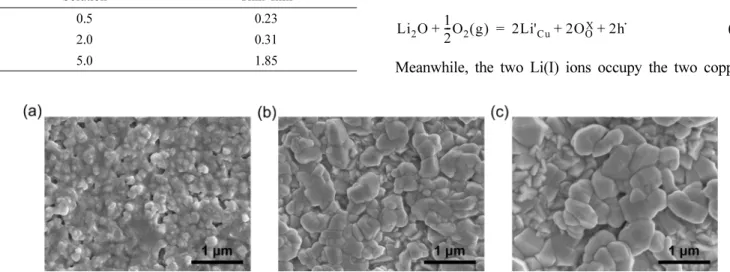
oC. The surface morphologies of the prepared CuO thin films have been observed by FE-SEM (Fig. 1).
The film prepared with 400
oC-calcination is found to be composed of the smallest grains with a diameter of ca.
100 nm. As calcination temperature increased from 400 to 500 to 600
oC, the grain size for the film gradually increased from 100 to 300 to 400 nm. In addition, the CuO thin films doped with 0.23, 0.31, and 1.85 at% Li(I) (Cu
0.9977Li
0.0023O, Cu
0.9969Li
0.0031O, and Cu
0.9815Li
0.0185O) were prepared with equal thickness by the sol-gel coating method, using the solutions formulated with various Li(I)
concentrations [0.5, 2.0, and 5.0 at% vs. Cu(II)], at various calcinaiton temperatures, as shown in Table 1 with the composition analysis results by ICP-AES.
The surface morphology and its calcination-temperature dependence for the Li(I)-doped CuO thin films were rarely affected by Li(I) concentration, maybe because of intrinsically low doping concentration [<2 at% vs. Cu(II)]
of Li(I) for the CuO thin films. Indeed, a solubility limit of Li(I) in CuO lattice is very low (ca. 1.7 at%).
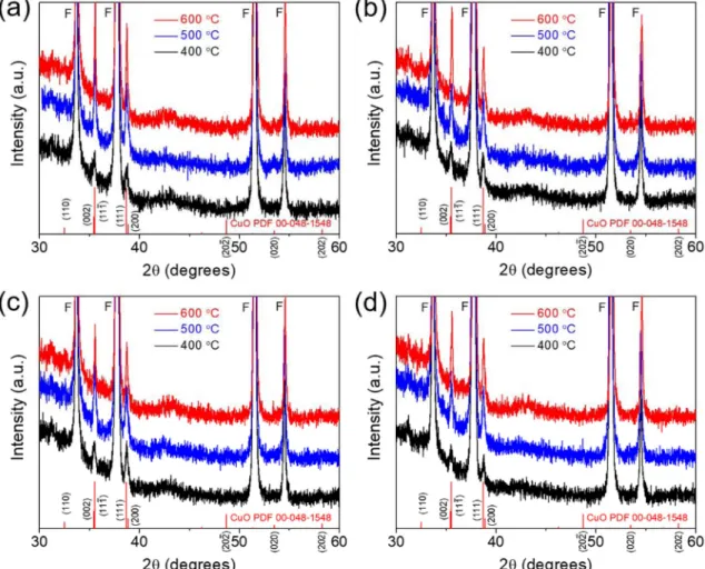
18)All the films revealed the characteristic XRD peaks for a polycrystalline CuO without any second phase and impurity (Fig. 2). Strengthening in the peak intensities with calcination temperature was observed regardless of Li(I) doping concentration, indicating the improvement of film crystallinity. Since Li(I) is known to substitute for Cu(II) in CuO lattice, the shift in 2θ position for the XRD peaks with a change in lattice parameter is expected.
4,18-21)However, the XRD peaks obtained for thin films are rather rough, and thus additional structure refinements are omitted in this work. Nevertheless, the substitutional doping of Li(I) into CuO can be well understood by defect chemistry. The native point defects of pristine CuO are doubly ionized copper vacancies (V''
Cu), granting intrinsic p-type semiconducting properties to CuO with an increase in hole density.
4,22,23)The corres- ponding reaction equation using Krӧger-Vink notation is as follows.
(1) The substitution of Li(I) for the CuO lattice involves the following two reactions (2) and (3) in preserving the equilibrium of reaction (1). The two Li(I) ions in Li
2O occupy normal Cu(II) sites and an oxygen atom is ionized from the gas phase to fill the second anion site.
Finally, two holes are generated:
(2) Meanwhile, the two Li(I) ions occupy the two copper
1
2---O2( )g = OOX+V''Cu+2h.
Li2O 1 2---O2( )g
+ = 2Li'Cu+2OOX+2h.
Fig. 1. FE-SEM top-view micrographs of the pristine CuO thin films prepared on FTO-glass substrates with a calcination process at (a) 400oC, (b) 500oC, and (c) 600oC, respectively.
Table 1. The amount of Li(I) added to the solution for sol-gel coating and their concentrations in the formed thin films, measured by ICP-AES.
Li(I) concentration (at%)
Solution Thin film
0.5 0.23
2.0 0.31
5.0 1.85
vacancies and extra oxygen from Li
2O is evolved as oxygen gas, where V''
Cuis consequently consumed:
(3) Therefore, the Li(I) doping into CuO leads to the reduction of copper-vacancy concentration and the enhancement of hole density, resulting in the increase of electronic hole conductivity in the p-type semiconductor CuO.
Furthermore, the characteristic negative enthalpy of the defect generation reaction in p-type semiconductor CuO indicates that the intrinsic defect density and electrical properties of CuO can be modulated by varying calcination temperature.
13,15,16)Specifically, the concentration of the intrinsic defects (copper vacancies) and electronic holes decreases with increasing calcination temperature, resulting in the decrease of electronic hole conductivity in the p-type semiconductor CuO.
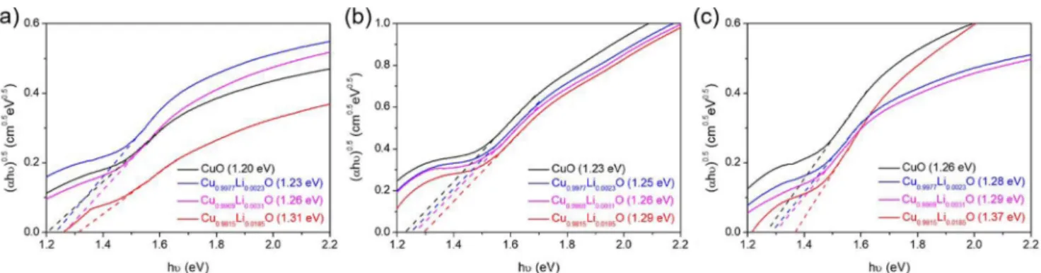
The indirect band gap energies (m = 2) of the undoped/
doped CuO thin films were estimated by the measurements of the optical absorbance using UV-vis-NIR diffuse reflectance spectroscopy. The resulting band gap energies obtained using the Eq. (4) are comparatively displayed with the Tauc plots in Fig. 3.
(4) where α, ν, E
g, and m are the absorption coefficient, optical frequency, band gap energy, and the characteristic transition value, respectively. Notably, the band gap energy of the pristine CuO thin film increased slightly from 1.20 to 1.23 to 1.26 eV with increasing calcination temperature from 400 to 500 to 600
oC. The p-type semiconducting property of pristine CuO, which Fermi level is located near the valence band maximum, is formed with the defect band tail by the native point defect, V''
Cu. As aforementioned, with increasing calcination temperature for the CuO thin film, the concentration of the native point defects and electronic holes decreases. It results in
Li2O 2V''+ Cu 2Li'Cu 12---O2( )g +
=
αhv = A hv E( – g)m
Fig. 2. XRD patterns acquired for the CuO thin films prepared at various calcination temperatures of 400, 500, and 600oC with varying Li(I) doping concentration of (a) 0 at% (pristine CuO), (b) 0.23 at%, (c) 0,31 at%, and (d) 1.85 at% vs. Cu (“F” marks represent the peaks arising from the FTO-glass substrate). The bottom bars are JCPDS standard for polycrystalline CuO (no. 48-1548).
the elimination of defect band tail and thus the widening of optical band gap, as reported previously.
24)Hence, the absorption edge shifts to higher energy and the apparent optical band gap increases. Such a calcination-temperature dependence on the concentration of the native point defects and electronic holes, observed in pristine CuO, showed the same trend for the CuO thin films doped with Li(I). Another important finding is that the band gap increases gradually with increasing the Li(I) concentration for the CuO thin film. It can be easily understood on the basis of the Burstein-Moss effect, demonstrating that higher carrier concentration results in a higher optical band gap.
4,25,26)Since the Li(I) ion acts as a shallow acceptor with a low formation energy in CuO lattice,
22)the hole density increases with increasing the Li(I) concentration in CuO. In the degenerate p-type semiconductor CuO with the high hole density, Fermi level lies inside valence band.
4)In this case, electrons transit from valence band located below the Fermi level into the top of conduction band. Therefore, the absorption edge shifts to higher energy and the apparent optical band gap increases. Interestingly, the band gap of Li(I)-doped CuO thin films increases with increasing calcination temperature. It might be attributed to the elimination of the intrinsic defect level despite the decrease of the intrinsic hole density.
The chemical composition of the undoped or 1.85 at% Li(I)-doped CuO thin films prepared with various calcination temperatures has been characterized by XPS, and the Cu2p and O1s core level spectra were acquired (Fig. 4) (the 500
oC-calcined film has been more specifically investigated with Li(I) doping of 0.23, 0.31, and 1.85 at%). The Cu2p spectra for all the films consist of the spin-orbit split 2p
1/2and 2p
3/2peaks with the shake-up satellite peaks on their left sides (higher binding energies), indicating the characteristic of Cu(II) oxide in CuO.
4,13,27)It is, first, found that the binding energy of Cu2p
3/2peak acquired for the film slightly increases as calcination temperature increases from 400
to 500 to 600
oC; it shifts from 931.75 to 932.70 to 932.85 eV for bare CuO film and from 932.40 to 933.20 to 933.50 eV for 1.85 at% Li(I)-doped CuO film [Fig. 4 (a), (c), and (e)]. Also, the Li(I) doping into CuO appears to increase the binding energies of Cu2p
3/2peak for the CuO films throughout the calcination temperature; it shifts from 931.75 [no Li(I)] to 932.40 eV [1.85 at%
Li(I)] for 400
oC-calcined film [Fig. 4(a)], from 932.70 [no Li(I)] to 933.20 eV [1.85 at% Li(I)] for 500
oC- calcined film [Fig. 4(c)], and from 932.85 [no Li(I)] to 933.50 eV [1.85 at% Li(I)] for 600
oC-calcined film [Fig.
4(e)]. Such a shift in the binding energy of Cu2p
3/2peak is believed to result from the modulated Fermi level energy by the substitution of Li(I) acting as a shallow acceptor and by decreasing the concentration of the copper vacancies generating Cu(I) component.
4,14,28)Meanwhile, the O1s spectra due to the lattice oxygen bound to Cu(II) in CuO are constantly observed near 529.40 eV for all the films [Fig. 4(b), (d), and (f)].
4,29)The peaks at 531.10 eV observed for all the films arise from the surface metal hydroxides or carbohydrates.
29)In particular, it indicates the existence of lithium hydroxides or carbohydrates by Li(I) doping as well as copper hydroxides or carbohydrates on the film surface.
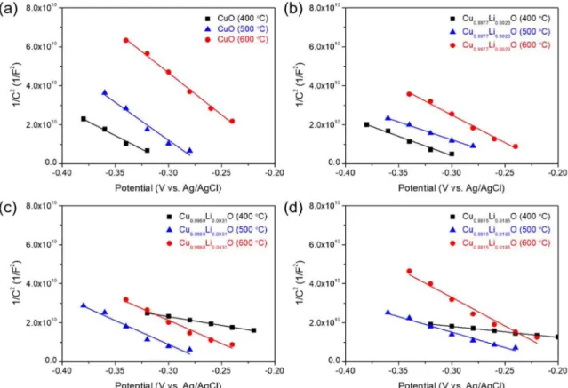
29)The hole density of the films was determined by the Mott-Schottky analysis using electrochemical impedance method at 1 kHz. The Mott-Schottky plots have been acquired for the films with varying calcination temperature and Li(I) concentration (Fig. 5). The negative slopes are observed for all the films, indicating that those films work as a p-type semiconductor. The hole density (N
A) can be obtained from the slope of the Mott-Schottky plot on the basis of the following Eq. (5).
30,31)(5) where C is capacitance, e is the electron charge, ε is the dielectric constant of CuO (ε = 10.26),
31)ε
0is the permittivity
1 C2
--- 2 eεε0A2NA ---
⎝ ⎠
⎛ ⎞ V V( – FB) KBT ---e –
=
Fig. 3. Tauc plots of the undoped/Li(I)-doped CuO thin films prepared at various calcination temperatures of (a) 400, (b) 500, and (c) 600oC.
of vacuum, A is the surface area, V is the electrode potential, V
FBis the flat band potential, K
Bis Boltzmann constant, and T is temperature. The slope, 2/eεε
0A
2N
A, shows a negative value from e and it is reduced negatively (the absolute value of the slope is reduced) as N
Aincreases. Although the hole density values obtained
here by the Mott-Schottky analysis on the semiconductor/
electrolyte interface might not be equal to those on the semiconductor/air interface for an actual gas sensor circumstance, this analysis enables the comparison of the relative hole density on the films.
The gas sensing properties of the CuO thin films have
Fig. 4. XPS spectra of (a) Cu2p and (b) O1s acquired for the undoped and 1.85 at% Li(I)-doped CuO thin films prepared with calcination at 400oC. XPS spectra of (c) Cu2p and (d) O1s acquired for the undoped, 0.23, 0.31, and 1.85 at% Li(I)-doped CuO thin films prepared with calcination at 500oC. XPS spectra of (e) Cu2p and (f) O1s acquired for the undoped and 1.85 at% Li(I)-doped CuO thin films prepared with calcination at 600oC.been investigated toward ethanol (C
2H
5OH) gas balanced with air at operating temperature of 300
oC. The stable and reversible response transients toward C
2H
5OH gas were obtained under the cross-input conditions of the air and C
2H
5OH gas with the various concentrations of 1,000-50 ppm, guaranteeing the stability, the reproducibility, and the gas-concentration dependence of the CuO thin film sensor [Fig. 6(a)]. A further multiple cycling test identified the short-term stability of the sensor. In Fig.
6(b), the gas response transients to 1,000 ppm C
2H
5OH acquired for the CuO thin film gas sensors prepared at various calcination temperatures of 400, 500, and 600
oC with varying Li(I) doping concentration of 0 at% (pristine CuO), 0.23, 0,31, and 1.85 at% vs. Cu are shown. The obtained gas response values are plotted as a funciton of Li(I) concentration in Fig. 7(c). The undoped/doped CuO thin film sensors exhibited a typical p-type sensing behavior with the increases of electrical resistance toward the reducing C
2H
5OH gas.
The gas sensing principle of the p-type CuO sensor toward the reducing C
2H
5OH gas can be described as follows. The atmospheric O
2gas is adsorbed in the form of O
-ions on the surface of CuO at 200
oC and over, with the following reactions.
13,32)(6)
(7) These reactions generate the hole-accumulation layer in the surface region of CuO grains in air, reducing the sensor resistance. When the sensor is exposed to the reducing C
2H
5OH gas, the surface chemical reaction is as follows:
(8) The adsorption of the reducing C
2H
5OH gas onto the CuO surface decreases the width of hole-accumulation layer in the surface region of CuO and therefore increases the sensor resistance. Such a change in the resistance depending on the gas adsorption and desorption serves as a signal for the gas response, which can be defined as the ratio (R
g/R
a) of the resistance in a target gas (R
g) to that in air (R
a) that is obtained from the measured response transient curves.
The hole density (N
A) values were obtained by fitting the linear slopes of the Mott-Schottky plots measured experimentally in Fig. 5 and using Eq. (5). Fig. 5 shows that the negative slope of the Mott-Schottky plot acquired for the 400
oC-calcined film was reduced gradually with increasing Li(I) concentration to 0.31 at% vs. Cu(II),
adsorption
gas O
O) 2( )
( 2 ↔
adsorption lattice
adsorption e O
O) ( ) ( )
( + − ↔ −
−
− → + +
+ O CO H O e
OH H
C )gas 6( )adsorption 2( )gas 3( )gas 6
( 2 5 2 2
Fig. 5. Mott-Schottky plots acquired for the CuO thin films prepared at various calcination temperatures of 400, 500, and 600oC with varying Li(I) doping concentration of (a) 0 at% (pristine CuO), (b) 0.23 at%, (c) 0,31 at%, and (d) 1.85 at% vs. Cu.
indicating a gradual increase of the hole density [Fig.
7(a)]. However, its increment a little moderated at Li(I) concentration over 0.31 at%. In particular, the films calcined at 500 and 600
oC exhibited roughly saturated hole density values at Li(I) concentration over 0.31 at%.
It suggests that all the added Li(I) ions over 0.31 at% are
not lattice-substituted for CuO and some are likely to
exist as segregations or precipitations. Furthermore, as the
calcination temperature of film increases, the variation in
hole density for the film decreases; even, the hole density
Fig. 6. (a) Response transients of the 400oC-calcined 1.85 at% Li(I)-doped CuO thin film gas sensor toward C2H5OH (1000-50 ppm) acquired at operating temperature of 300oC. (b) Gas responses to 1000 ppm C2H5OH acquired for the CuO thin film gas sensors prepared at various calcination temperatures of 400, 500, and 600oC with varying Li(I) doping concentration of 0 at% (pristine CuO), 0.23, 0,31, and 1.85 at% vs. Cu. The operating temperature is 300oC.value for the 600
oC-calcined film is slightly reduced with the reversal of the slope of the Mott-Schottky plot at high Li(I) concentration of 0.31-1.85 at% [Fig. 5 and Fig. 7(a)]. It is believed to be caused by the offset effect of hole density due to the decrease of intrinsic hole density with increasing the calcination temperature and the increase of extrinsic hole density with increasing the Li doping amount.
Meanwhile, the film calcined at a low temperature of 400
oC showed an increase of electrical resistance by Li(I) doping in spite of the dramatic increase in hole density [Fig. 7(b)]. It is attributed to an extremely lowering hole mobility by a high concentration of structural defects [copper vacancies, Li(I) dopants, and grain boundaries]
in the film. Actually, as calcination temperature increased from 400 to 500 to 600
oC, the grain size for the film gradually increased from 100 to 300 to 400 nm, as observed by FE-SEM (Fig. 1). It indicates that the film prepared at lower calcination temperature has more grain boundaries working as the structural defect lowering hole mobility. Furthermore, in this work, the Li(I)-doped CuO thin films have been prepared with the substitution of Li(I) for Cu(II) through heat treatment of Li(I)-Cu(II) ionic gel films in air. In this case, Li(I) excess can exist in the form of precipitation of lithium hydroxides or carbohydrates on surfaces or at grain boundaries of the thin films. Indeed, the XPS O1s spectra acquired for the Li(I)-doped CuO thin films in Fig. 4 implied the existence of lithium hydroxides or carbohydrates on the film surface.
Also, such Li(I) excess species can be precipitated at grain boundaries in the same form for all Li(I)-doped CuO thin films although the additional characterization is needed (even if such a hypothesis is wrong, the relative comparison of the characteristics between the samples will not be affected). As a result, such Li(I) excess species formed on surfaces or at grain boundaries can affect the overall resistance of the films and therefore it is included in the structural defects, mentioned above. In
contrast, the film calcined at a high temperature of 600
oC exhibited the resistance behavior decreasing with increasing hole density upon the Li(I) doping due to the low concentration of structural defects. Such a conflicting effect between hole density and structural defects for the sensor resistance maintains the resistance of the film calcined at the intermediate temperature of 500
oC somewhat constantly. In particular, it is found that the gas response values of the films, measured for 1000 ppm C
2H
5OH at 300
oC, are directly proportional to the apparent sensor resistance [Fig. 7(c)]. The apparent resistance increases with increasing the concentration of structural defects in the film. Such structural defects involving metal/oxygen vacancies, dopants, and grain boundaries in the film can work as reaction sites for gas sensing.
4,10-14)As a result, since the CuO thin film prepared with the lowest calcination temperature (400
oC) and the highest Li(I) concentration (1.85 at% vs. Cu) shows the highest apparent resistance with the highest concentration of structural defects, its gas response shows the maximum value of 4.32. The gas response values obtained in this work are not remarkable since the purpose of this work is the mechanistic study for gas sensing.
Significantly, these results mean that the gas response
characteristic of the oxide semiconductor gas sensors
depends primarily on the concentration of structural
defects including point defects (copper vacancies, oxygen
vacancies, and dopants) and grain boundaries, regardless
of hole carrier density. It well explains the previously
reported results: high gas response characteristics of the
pristine CuO film with high intrinsic copper-vacancy
concentration and high hole density,
13)the response
characteristic degraded by the lower-valent cation doping
decreasing copper-vacancy concentration and increasing
hole density, and the response characteristic enhanced by
the higher-valent cation doping increasing copper-vacancy
concentration and decreasing hole density.
4)That is, the
gas response characteristic in all cases is only proportional
Fig. 7. (a) Hole density and (b) sensor resistances (measured at 300oC in air) plotted as a function of Li(I) doping concentration for the CuO thin films prepared at various calcination temperatures of 400, 500, and 600oC. (c) Their gas responses toward 1000 ppm C2H5OH plotted as a fuction of Li(I) doping concentration, measured at 300oC.to the concentration of structural defects such as copper vacancies that can work as reaction sites for gas sensing, independently of hole density. However, it runs counter to the commonly known electronic sensitization mechanism that the decrease in the carrier density increases the depletion-layer width of grains, leading to the increase in gas response (or magnitude of resistance change) toward reducing gases.
4,17)4. Conclusion
The gas response characteristic toward the reducing C
2H
5OH gas has been demonstrated in terms of copper- vacancy concentration, hole density, and microstructural factors for the undoped/Li(I)-doped CuO thin films prepared by the sol-gel method. For the films, both concentrations of intrinsic copper vacancies and electronic holes decrease with increasing calcination temperature from 400 to 500 to 600
oC. The substitution of Li(I) for Cu(II) in CuO results in the apparent increase of hole density while consuming copper vacancies. The increase of calcination temperature or Li(I) doping concentration in the film increases the optical band gap energy. As a consequence, it is found that the gas response value of film sensor is monotonously proportional to the apparent sensor resistance, which is determined by the concentration of the structural defects such as copper vacancies, Li(I) dopants, and grain boundaries rather than hole density.
Acknowledgements
This work was supported by the National Research Foundation of Korea (NRF) grant funded by the Korea government (MSIT) (No. 2019R1G1A1006231).
References
1. X. Zhou, S. Lee, Z. Xu and J. Yoon, Chem. Rev., 115, 7944 (2015).
2. M. Righettoni, A. Amann and S. E. Pratsinis, Mater.
Today, 18, 163 (2015).
3. N. Barsan, D. Koziej and U. Weimar, Sens. Actuators B, 121, 18 (2007).
4. Y.-H. Choi, D.-H. Kim, S.-H. Hong, Sens. Actuators B, 243, 262 (2017).
5. I. A. Alagdal and A. R. West, J. Mater. Chem. C, 4, 4770 (2016).
6. M. M. Natile, A. Ponzoni, I. Concina and A. Glisenti, Chem. Mater., 26, 1505 (2014).
7. J.-H. Lee, Sens. Actuators B, 140, 319 (2009).
8. G. Korotcenkov, Mater. Sci. Eng. B, 139, 1 (2007).
9. M. Batzill and U. Diebold, Prog. Surf. Sci., 79, 47 (2005).
10. M.-W. Ahn, K.-S. Park, J.-H. Heo, J.-G. Park, D.-W.
Kim, K. J. Choi, J.-H. Lee and S.-H. Hong, Appl. Phys.
Lett., 93, 263103 (2008).
11. S. Maeng, S.-W. Kim, D.-H. Lee, S.-E. Moon, K.-C.
Kim and A. Maiti, ACS Appl. Mater. Interfaces, 6, 357 (2014).
12. B. Tong, Z. Deng, B. Xu, G. Meng, J. Shao, H. Liu, T.
Dai, X. Shan, W. Dong, S. Wang, S. Zhou, R. Tao and X. Fang, ACS Appl. Mater. Interfaces, 10, 34727 (2018).
13. Y.-H. Choi, D.-H. Kim, S.-H. Hong and K. S. Hong, Sens. Actuators B, 178, 395 (2013).
14. Y.-H. Choi, D.-H. Kim and S.-H. Hong, ACS Appl.
Mater. Interfaces, 10, 14901 (2018).
15. A. Cruccolini, R. Narducci and R. Palombari, Sens.
Actuators B, 98, 227 (2004).
16. Y. K. Jeong and G. M. Choi, J. Phys. Chem. Solids, 57, 81 (1996).
17. H.-J. Kim and J.-H. Lee, Sens. Actuators B, 192, 607 (2014).
18. X. G. Zheng, H. Yamada, D. J. Scanderbeg, M. B. Maple and C. N. Xu, Phys. Rev. B, 67, 214516 (2003).
19. S. Suda, S. Fujitsu, K. Koumoto and H. Yanagida, Jpn.
J. Appl. Phys., 31, 2488 (1992).
20. N. Yoshida, T. Naito and H. Fujishiro, Jpn. J. Appl.
Phys., 52, 031102 (1992).
21. X. G. Zheng, H. Yamada, D. J. Scanderbeg, M. B. Maple and C. N. Xu, Phys. Rev. B, 67, 214516 (2003).
22. Y. Peng, Z. Zhang, T. V. Pham, Y. Zhao, P. Wu and J.
Wang, J. Appl. Phys., 111, 103708 (2012).
23. E.A. Goldstein, T. M. Gür and R. E. Mitchell, Corros.
Sci., 99, 53 (2015).
24. Y. Wang, P. Miska, D. Pilloud, D. Horwat, F. Mücklich and J. F. Pierson, J. Appl. Phys., 115, 073505 (2014).
25. E. Burstein, Phys. Rev., 93, 632 (1954).
26. T. S. Moss, Proc. Phys. Soc. (Lond.), B67, 775 (1954).
27. C. C. Chusuei, M. A. Brookshier and D. W. Goodman, Langmuir, 15, 2806 (1999).
28. Y.-H. Choi, D.-H. Kim and S.-H. Hong, Sens. Actuators B, 268, 129 (2018).
29. National Institute of Standards and Technology (NIST), NIST X-ray Photoelectron Spectroscopy Database. From http://srdata.nist.gov/xps/, 2012, Retrieved September 1, 2019
30. S. Kamimura, N. Murakami, T. Tsubota and T. Ohno, Appl. Catal. B, 174, 471 (2015).
31. C.-Y. Chiang, Y. Shin and S. Ehrman, J. Electrochem.
Soc., 159, B227 (2012).
32. A. Bejaoui, J. Guerin and K. Aguir, Sens. Actuators B, 181, 340 (2013).
< 저자소개 >
최윤혁
대구가톨릭대학교 공과대학 신소재화학공학부 교수