http://dx.doi.org/10.3938/NPSM.69.128
Design and Fabrication of a Low-Cost Teaching Atomic Force Microscope with 3D Printed Parts
Melody Chepkoech · Bernard Ouma Alunda · Luke Oduor Otieno
· Sang Joon Park · Clare Chisu Byeon · Yong Joong Lee
∗School of Mechanical Engineering, Kyungpook National University, Daegu 41566, Korea (Received 11 December 2018 : accepted 17 December 2018)
Over the past decade, additive manufacturing and three-dimensional (3D) printing have had a profound impact on manufacturing. With the emergence of affordable 3D printers, rapid prototyping has been quite accessible to researchers in academic and industrial laboratories. As a consequence, the number of laboratory instruments that have been assembled with 3D printed parts has risen. We present an atomic force microscope (AFM) constructed with as many 3D printed parts as the design would permit. Due to its simplicity, the proposed AFM is suitable for assembly by undergraduate students in a project-based laboratory course setting. The images of compact disc (CD) data tracks and standard samples obtained using the proposed low-cost AFM effectively demonstrate its nanoscale imaging capability.
PACS numbers: 68.37.Ps, 07.79.Lh
Keywords: Atomic force microscopy, Scanner, 3D printers
I. INTRODUCTION
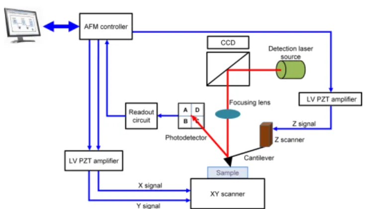
Since its invention in 1986 by Binnig et al. [1], the atomic force microscope (AFM) has remained to be an indispensable tool in nano-scientific research and tech- nology [2,3]. Its versatility is evidenced by the wide appli- cations in air, liquid, and vacuum environments [4]. Ad- ditionally, it can be used to image surfaces of both con- ductive and non-conductive materials [5]. Fig. 1 shows a schematic diagram of an AFM showing essential compo- nents: a light source, a cantilever with a sharp tip, pho- todetector, scanners, and an electronic AFM controller.
When a flexible cantilever with a sharp tip at its end is brought into close proximity or in contact with the sample, the interaction between the tip and the sample results in repulsive or attractive forces. The attractive forces are due to van der Waals forces whereas the re- pulsive forces originate from two atoms that are so close to one another such that their electron orbitals begin to interact with each other. These interaction forces cause
∗E-mail: [email protected]
Fig. 1. (Color online) Schematic of AFM showing various components.
the cantilever to deflect [6–9], and the deflection of the cantilever is measured by the position sensitive photode- tector (PSPD). The photo-induced currents from the photodetector are then converted into voltages by the electronic readout circuit that typically involves trans- impedance amplifiers. The feedback controller from the AFM control electronics maintains a constant separation between the tip and the sample by maintaining a con- stant deflection of the cantilever, and the voltage output
This is an Open Access article distributed under the terms of the Creative Commons Attribution Non-Commercial License (http://creativecommons.org/licenses/by-nc/3.0) which permits unrestricted non-commercial use, distribution, and reproduction in any medium, provided the original work is properly cited.
a reasonable level of precision machining and therefore costly. Due to the complexity and the level of precision required for producing AFM components, the atomic force microscope typically remains inaccessible for most undergraduate students.
There have been a few attempts to design simplistic AFMs used for teaching undergraduate students. Bon- son et al. developed working model demonstrating prin- ciple of an AFM by using a phonograph stylus to replace the AFM cantilever and tip [10]. However, the resolu- tion of their setup was greatly limited by the size of the phonograph stylus to about 20 µm. A conceptual AFM operating on a macroscale level using LEGO® bricks has been developed by Hsieh and his co-workers [11]. The resolution of the rotational motors driving the X-Y mo- tion platform limited the lateral resolution and the ver- tical resolution was limited to 2.05 mm. The low-cost AFM proposed by Bergmann et al. [12] using Fabry- Perot as a detection method on the other hand operated on a constant height mode making it transparent and less complex by removing the feedback control. However, the system could only detect features below 158 nm limited by the maximum signal achievable interference pattern.
Siu et al. developed an optical beam deflection teaching AFM using most parts available in a common laboratory set-up [13]. However, the AFM setup had a relatively limited scanning speed and a lateral as well as a vertical resolution below 20 nm. Although the aforementioned works attempted to develop simplistic teaching AFMs, the construction was mostly done with commercial com- ponents. In this work, we describe a low-cost teaching AFM in which the critical components such as the scan- ner and the translational stages are fabricated with a 3D printer.
II. AFM DESIGN
The key components of an AFM are X-Y and Z scan- ners, mechanical translation stages required to align the
duced with a 3D printer.
1. Scanners
The X-Y and Z scanners are arguably the most criti- cal components of the AFM because they determine the resolution of the overall system. The scanner design has an effect on the achievable scan range, scan speed, and the quality of the obtained images. In the past, most commercial AFMs used tripod, tube, or conical scan- ners [14]. Tripod scanners were effective but they are usually large and bulky. Moreover, they are relatively prone to thermal drifts and mechanical vibrations [15].
The piezoelectric tube scanner is one of the most com- monly used AFM scanners [16,17]. Despite the low-cost and large scan range, piezoelectric tube scanners have limited bandwidths, are sensitive to thermal drifts, and have high degrees of cross-coupling between the lateral and vertical axes. Conical scanners, on the other hand have higher resonance frequencies and large scan range compared to piezoelectric tube scanners due to their tri- angular cross-sectional shape [18,19]. However, these scanners are quite expensive and difficult to manufac- ture. Due to the limitations of the aforementioned scan- ners, flexure-based scanners have been developed and are widely used [20–23] in recent years. The fine motions by these scanners is achieved through the elastic deforma- tion of the flexures. The thickness of the flexures deter- mines the stiffness and therefore the maximum possible scan range. Most importantly, these scanners do not have any moving joints so problems such as backlash, friction, and wear which are common in traditional me- chanical joints are completely eliminated. A high level of repeatability, which is one of the most desirable features of nanopositioning stages, is also achieved.
There are two kinematic configurations used in flexure- based scanners, serial kinematic and parallel kinematic configurations. In the parallel kinematic configuration,
Fig. 2. (Color online) The isometric views of (a) 3D CAD model and (b) 3D printed part of the X-Y scanner, and (c) 3D CAD model and (d) 3D printed part of the Z scanner.
the axes are independent of each other whereas in the serial kinematic configuration, the fast (X) axis is em- bedded in the slow (Y) axis. In this work, the serial kinematic scanner configuration was adopted because of its ease of fabrication and simplicity. Each axis of the scanner adopts an amplifying lever mechanism. For a lever arm of length, L, the amplification is given by L/a, where a is the distance between the hinge and the po- sition of the piezoelectric actuator. Fig. 2(a) shows the 3D CAD model of the X-Y scanner developed in this re- search. The overall size of the scanner is 137 × 113.5 mm2 with the central moving platform of the size 20 × 20 mm2. Corner filleted flexure hinges were adopted in the scanner design because of the ease of printing com- pared to the circular cutout hinges [24]. Fig.2(b) shows the 3D printed X-Y scanner with piezoelectric actuators installed. The X axis is driven by a piezoelectric ac- tuator (Thorlabs Inc., part # AE0505D16F) with the unloaded resonant frequency of 69 kHz, stiffness of 48.9 N/µm, blocking force of 850 N, and the stroke of 17 µm with the drive voltage of 150 VDC. On the other hand, the Y axis is driven using a piezoelectric actua- tor (Thorlabs Inc., Part # AE0505D44H40DF) with the unloaded resonant frequency of 24 kHz, stiffness of 20.2 N/µm, blocking force of 850 N, and the stroke of 42 µm with the drive voltage of 150 VDC. Pre-loading of the
Fig. 3. (Color online) Experimental setup used for scan range and hysteresis measurements for the X-Y and Z scanners.
piezoelectric actuators was achieved by using a combi- nation of a fine pitch adjustment screw (Thorlabs Inc., Part # F3ES20) and a threaded bushing (Thorlabs Inc., Part # F2ESN1P). Pre-loading was done to compensate for inertial loads that are generated during the scanning process [25,26].
The Z scanner helps to regulate the interaction forces between AFM probe with respect to the sample and pre- vents the application of excessive forces that may damage the cantilever tip during scanning. We separated the X- Y and Z scanners to prevent the effect of cross-coupling between the lateral and the vertical axes during scan- ning. Fig.2(c) and (d) show the 3D CAD model and the assembled Z scanner, respectively.
2. Scanner Characterization
Measurement of the scan range is an essential pro- cess in scanner characterization because the calibration constant which relates the applied voltage to the scan- ner stroke can be derived. A capacitive sensor (ADE Technologies Model 5810) was used to measure the scan ranges of both X-Y and Z scanners. Capacitive sensors are cost effective, have good resolution, low noise and high sensitivity. The experimental setup used to mea- sure the maximum stroke of the scanners is shown in Fig. 3. The voltage was varied from 0 V to 100 V in each axis of the X-Y scanner while the actual displace- ment of the square moving platform was measured. The measured maximum stroke of the 3D printed X-Y scan- ner was found to be 14 µm and 21 µm in the X and Y axis, respectively. The maximum scan range of the Z scanner was 3.4 µm. Although the travel range of our X- Y scanner is smaller than typical commercial scanners, it
Fig. 4. (Color online) Measured hysteresis loops: (a) fast (X) axis and (b) slow (Y) axis of the X-Y scanner and (c) Z scanner.
is sufficient enough for imaging data tracks of CD, DVD, or even Blu-ray disks.
The 3D printed X-Y and Z scanners are operated in the open loop configuration. Therefore, the hysteresis was not compensated. A large amount of hysteresis de- creases the positioning accuracies during scanning neg- atively affecting the fidelity of images obtained. There- fore, we measured the amount of hysteresis inherent in both X-Y and Z scanners, and the results showing the hysteresis loops in both scanners are presented in Fig.4.
Hysteresis was quantified by determining the root-mean- square errors (RMSE) as well as the tracking error emax
also known as the percentage maximum absolute er- ror (MAE). Eq. (1) was used to compute emax values whereas Eq. (2) was used to compute the RMSE val- ues. The approximated value of RMSE was found to be 6.28%, 8.14% and 12.90% in the X, Y, and Z axes, respectively. The emax value was calculated as 10.7%,
Hysteresis, emax (%) 10.7 13.7 6.69
13.7% and 6.69% in the X, Y, and Z axes, respectively.
These results have been summarized in Table1.
emax = max|y − r|
max y− min y× 100% (1) RMSE(%) =
√
1 N
∑N
i=1(yi− ri)2
max y− miny × 100% (2)
where y = [y0, y1, . . . , yN−1] and r = [r0, r1, . . . , rN−1] and N is the number of points used in the measurements.
3. Mechanical Design
Developing a scan head of a low-cost atomic force mi- croscope involved designing of various mechanical trans- lation stages needed for positioning of several optical parts with respect to one another. Also, some mechanical parts for holding optical parts were needed to be designed and fabricated. Finally, the overall external housing is needed as a skeleton on which various mechanical and optical components can be attached.
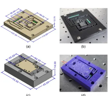
Fig. 5(a) and (b) show the 3D CAD model and 3D printed single-axis translation stage, respectively. The translation stage has two guiding rods that together with a tension spring constrains the motion of the moving platform in one direction. The single-axis translation stage was used to bring the cantilever into focus during alignment of the detection laser. Tap holes are provided for mounting the Z scanner. The 3D CAD model of a two-axis translation stage developed for the AFM is shown in Fig. 5(c). The translation stage was used for X-Y movement of the detection laser against a station- ary cantilever for alignment. The 3D printed two-axis translation stage is shown in Fig. 5(d). The design in- corporates a central hole to allow the passage of the laser beam from the beamsplitter towards the cantilever and four holes for mating the beamsplitter and the focusing
Fig. 5. (Color online) The isometric views of (a) 3D CAD model and (b) 3D printed single-axis translation stage, (c) 3D CAD model and (d) 3D printed X-Y trans- lation stage, (e) 3D CAD model and (f) 3D printed can- tilever holder, (g) 3D CAD model and (h) 3D printed tube mount for the focusing lens.
lens mount. Fig. 5(e) shows the 3D CAD model of the cantilever holder with a 16◦ angle orientation with re- spect to the horizontal surface. The angle ensures that only the tip of the probe touches the sample during scan- ning. The realized 3D printed cantilever holder is shown in Fig. 5(f). To simplify the alignment of the focusing lens and to achieve the focal length needed in our setup, we fabricated the focusing lens tube. Fig. 5(g) and (h) show the 3D CAD model and the 3D printed focusing
Fig. 6. (Color online) The isometric view of (a) 3D CAD model and (b) the realized low-cost teaching AFM.
lens tube.
The housing needed as a skeleton on which various mechanical and optical components of the low-cost AFM scan head was designed. The 3D CAD model of the as- sembly is shown in Fig. 6(a). The red dashed line in Fig. 6(a) indicates the optical path followed by the de- tection laser beam. In our design, a single mode optical fiber pigtailed laser diode (Thorlabs Inc., Part #LPS- 635-FC) mounted on a mount (Thorlabs Inc., Part # LDM9LP) was used as the laser source. The control of current and temperature of the laser diode was accom- plished using a laser diode controller (Stanford Research Systems, Model LDC500). The laser beam was colli- mated to a diameter of 0.8 mm by using a fiber colli- mator (Thorlabs Inc., Part # F230FC-B) with the focal length of 4.43 mm and numerical aperture (NA) of 0.56.
A large NA ensures that a larger amount of light can be collected by the lens. The collimated beam is then re- flected off a non-polarizing beamsplitter (Thorlabs Inc., Part # CM1-BS013) onto a focusing aspheric lens (Thor- labs Inc., Part # C280TME-B). The aspheric lens has the effective focal length of 18.4 mm, NA of 0.15 and
back of the cantilever is directed to the photodetector for deflection measurements. The realized working set-up of the developed AFM is shown in Fig.6(b).
4. Electronics and Controller Design
Interfacing of the scan head with the control electron- ics is another vital step in the operation of the AFM.
A quadrant photodetector (First Sensor, Part # QP50- 6 TO) with the active area of 4 × 12 mm2 was used.
A custom-built readout circuit was used to convert the photo-induced currents from the quadrant photodetector into voltage signals. Typically, three signals (vertical de- flection, horizontal deflection, and sum) from the readout circuit are required for proper functioning of the AFM.
The vertical deflection signal is obtained by subtracting the sum of the signals from the top two quadrants of the PSPD (A and D) from the sum of the signals from the bottom two quadrants (B and C). The horizontal signal was also obtained from the difference between the sum of the signals from the two left quadrants (A and B) and the two right quadrants (D and C). The sum signal is obtained by adding the signals from all four quadrants.
The vertical and the horizontal signals are helpful during laser alignment whereas the sum signal is used to mon- itor the strength of the laser power. Finally, LabVIEW FPGA-based real-time control code previously developed in our laboratory was used to control the various opera- tions of the AFM.
III. AFM IMAGING
After interfacing the scan head with the control elec- tronics, the operation of the developed low-cost teach- ing AFM was evaluated in order to ascertain the perfor- mance. First, alignment of the tightly focused detection laser beam at the back of the cantilever was done us- ing the 3D printed translational stages. The laser spot
Fig. 7. (Color online) (a) Topographical image of the calibration sample, (b) error-signal image, (c) 3D topo- graphical image, and (d) line profile along AA′shown in (a). All images were obtained in contact mode at the resolution of 128 pixels × 128 pixels.
should be positioned as close as possible to the cantilever free end to maximize the signal-to-noise ratio. Second, the reflected laser beam should be positioned at the cen- ter of the photodetector. This task is carried out by ensuring the horizontal and the vertical deflection sig- nals from the outputs of the readout circuit are close to 0 V.
Approaching and engaging of the probe tip onto the sample surface require a precise motion control. Fail- ure to control the fine motion may lead to damages to the probe tip and/or the sample. During the engage- ment process, the whole AFM head was lowered towards the sample while monitoring the vertical deflection sig- nal. The cantilever is considered engaged when the ver- tical deflection signal is as close as possible to the set- point value and variations can be compensated by the expansion or contraction of the Z scanner. The con- troller should monitor the deflection signals at a much faster rate than the lateral motion of the scanner during imaging. Otherwise the constant tip-sample interaction force can not be properly maintained. Our custom-built control platform involving real-time LabVIEW FPGA is capable of achieving the needed bandwidth.
We performed our first imaging of the calibration sam- ple with the lateral pitch of 10 µm and step height of
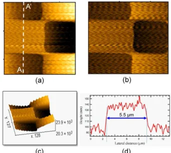
Fig. 8. (Color online) (a) Topographical image of CD data tracks, (b) error-signal image, (c) 3D topographical image, and (d) line profile along AA′ shown in (a). All images were obtained in contact mode at the resolution of 128 pixels ×128 pixels.
200 nm. Both the X-Y and Z scanners were operated in open-loop configuration. Contact mode images of 128 pixels × 128 pixels were obtained from the scan area of about 13× 13 µm2using a triangular cantilever (Bruker Inc., Part # NP-S). The raw topographical image is shown in Fig. 7(a), the error-signal image is shown in Fig.7(b) and the 3D image of the topography is shown in Fig. 7(c). A sectional cut (AA′) on the topograph- ical image (see Fig. 7(d)) shows that the approximate size of the plateau is about 5.5 µm which is close to the expected value of 5 µm. The discrepancy in the size of the plateau is mainly due to the effects of hysteresis. If a position measurement sensor such as capacitive sensor or a strain gauge sensor can be incorporated on the scan- ners in order to linearize the scanner travel, the quality of obtained images will improve significantly.
Imaging of samples with smaller features was also per- formed by scanning a compact disc (CD) with a nominal pitch of about 1.60 µm. A piece from a factory written CD was prepared by removing the protective layer in or- der to expose the data tracks. Similarly, contact mode imaging in air was done in open-loop configuration. An area of about 12× 12 µm2was imaged at the resolution of 128 pixels × 128 pixels. Fig. 8(a)-(c) shows the 2D
topographical image, error-signal image, and 3D image of the topography of CD, respectively. The line profile of a sectional cut (AA′) is shown in Fig. 8(d) and the measured track pitch was found to be about 1.70 µm, which is close to the nominal value of 1.60 µm.
IV. CONCLUSION
In conclusion, we have successfully developed a low- cost teaching atomic force microscope that is capable of imaging at nanoscale. Various mechanical components of the AFM have been successfully designed and 3D printed to replace the costly commercial counterparts. Our pro- posed design is simple enough for undergraduate stu- dents to assemble and test an AFM during a semester- long undergradaute laboratory course. However, in spite of its relative simplicity in design and limited operation in contact mode, our teaching AFM can be used to ob- tain surface images of the standard calibration sample and CD data tracks at submicron resolution. The con- cept of using 3D printed parts allows various possibilities for improvement and customization which can further entice the curiosity of students.
ACKNOWLEDGEMENTS
This work was supported by the National Research Foundation of Korea (NRF) grant funded by the Korea government (MSIT) (NRF-2018R1A2B6008264).
REFERENCES
[1] G. Binnig and D. P. E. Smith, Rev. Sci. Instrum.
57, 1688 (1986).
[2] T. Ando, N. Kodera, E. Takai, D. Maruyama and K. Saito et al., Proc. Natl. Acad. Sci. U.S.A. 98, 12468 (2001).
[3] S. Ramachandran and R. Lal, Indian J. Exp. Biol.
48, 1020 (2010)
[4] M. J. Doktycz, C. J. Sullivan, P. R. Hoyt, D. A.
Pelletier and S. Wu et al., Ultramicroscopy 97, 209 (2003).
(1999).
[9] D. Sarid and V. Elings, J. Vac. Sci. Technol. B. Mi- croelectron. Nanometer Struct. Process. Meas. Phe- nom. 9, 431 (1991).
[10] K. Bonson, R. L. Headrick, D. Hammond and M.
Hamblin, Am. J. Phys. 79, 189 (2011).
[11] T. H. Hsieh, Y. C. Tsai, C. J. Kao, Y. M. Chang and Y. W. Lu, Int. J. Autom. Smart Technol. 4, 113 (2014).
[12] A. Bergmann, D. Feigl, D. Kuhn, M. Schaupp and G. Quast et al., Eur. J. Phys. 34, 901 (2013).
[13] S. H. Loh and W. J. Cheah, Appl. Sci. 7, 226 (2017).
[14] G. Schitter and M. Rost, Mater. Today 11, 40 (2008).
[15] P. K. Hansma, V. B. Elings, O. Marti and C. E.
Bracker, Science 242, 209 (1988).
[16] B. Bhikkaji, M. Ratnam, A. J. Fleming and S. O.
R. Moheimani, IEEE Trans. Control Syst. Technol.
15, 853 (2007).
11, 110 (2009).
[19] B. O. Alunda, Y. J. Lee and S. Park, Instrum. Sci.
Technol. 46, 58 (2018).
[20] Y. K. Yong and S. O. R. Moheimani, in IEEE/ASME International Conference on Advanced Intelligent Mechatronics (AIM) (Montreal, Canada, 2010), p. 225.
[21] D. Kim, D. Kang, J. Shim, I. Song and D. Gweon, Rev. Sci. Instrum. 76, 073706 (2005).
[22] H. Tang and Y. Li, in IEEE/ASME International Conference on Advanced Intelligent Mechatronics (AIM) (Kaohsiung, Taiwan, 2012), p. 753.
[23] H. Tang and Y. Li, IEEE Trans. Robot. 29, 650 (2013).
[24] N. Lobontiu, J. S. N. Paine, E. Garcia and M. Gold- farb, J. Mech. Des. 123, 346 (2001).
[25] Y. K. Yong, S. O. R. Moheimani, B. J. Kenton and K. K. Leang, Rev. Sci. Instrum. 83, 121101 (2012).
[26] Y. K. Yong, Mechatronics 36, 159 (2016).