* Dept. of Electronics Engineering, Dankook University
★ Corresponding author
e-mail:[email protected], Tel:+82-31-8005-3625
※ Acknowledgment
“This research was supported by the MSIT(Ministry of Science and ICT), Korea, under the ITRC(Information Technology Research Center) support program(IITP-2020-2018-0-01421) supervised by the IITP(Institute for Information
& Communications Technology Planning & Evaluation)”, This work was supported by Circuit Technologies for High Speed Switching DC-DC Converters (10080622) funded by the Ministry of Trade, industry & Energy.
Manuscript received Jun. 6, 2020; revised Jun. 23, 2020; accepted Jun. 26, 2020.
This is an Open-Access article distributed under the terms of the Creative Commons Attribution Non-Commercial License (http://creativecommons.org/licenses/by-nc/3.0) which permits unrestricted non-commercial use, distribution, and reproduction in any medium, provided the original work is properly cited.
1200V급 4H-SiC Trench MOSFET의 Design parameter에 따른 전기적 특성 분석
Analysis of electrical characteristics according to the design parameter of 1200V 4H-SiC trench MOSFET
우 제 욱*, 서 정 주*, 진 승 후*, 구 용 서*★
Je-Wook Woo*, Jeong-Ju Seo*, Seung-hoo Jin*, Yong-Seo Koo*★
Abstract
Since SiC has 10 times higher breakdown field and 3 times higher energy gap than Si, it is possible to manufacture an excellent power MOSFET with a high breakdown voltage. However, since it has a high on-resistance due to low mobility, a Trench MOSFET has been proposed to lower it, but at the same time, it has a problem that BV decreases.
The purpose of this paper is to design a 1200V trench MOSFET, and to solve this, split Epi depth, Trench depth, and Trench depth to Epi depth, which are important variables for BV and Ron, to achieve maximum electric field, BV, Ron’s reliability characteristics were compared and analyzed. As the epi depth increased, the trench depth decreased, and the epi depth decreased at the trench depth, the maximum electric field decrease, BV increase, and Ron increase were confirmed. All results were simulated by sentaurus TCAD.
요 약
SiC는 Si에 비해서 Breakdown field가 10배 높고, Energy gap이 3배 높기 때문에 높은 Breakdown voltage를 갖는 우수한 전력 MOSFET을 제작할 수 있다. 하지만 낮은 Mobility로 인한 높은 On저항을 갖기 때문에 이를 낮추기 위해서 Trench MOSFET이 제안되었지만 동시에 BV가 감소한다는 문제점을 갖는다. 본 논문에서는 1200V급 Trench MOSFET 설계를 목 적으로 하며, 이를 해결하기 위해서 BV와 Ron에 대한 중요한 변수인 Epi 깊이, Trench 깊이, Trench 깊이에서 Epi 깊이까지 의 거리에 대한 Split을 진행하여 최대 전계, BV, Ron의 신뢰성 특성을 비교 분석하였다. Epi 깊이가 증가할수록, Trench 깊 이가 감소할수록, Trench 깊이에서 Epi 깊이가 감소할수록 최대 전계 감소, BV 증가, Ron 증가를 확인하였다. 모든 결과는 Sentaurus TCAD를 통해 Simulation 되었다.
Key words
:
SiC, Trench MOSFET, Electric field, Breakdown voltage, On-resistance221
Ⅰ. 서론
Silicon Carbide(SiC)는 Silicon(Si)에 비해, Breakdown field가 10배 높으며 Energy gap이 3배 높기 때문 에 높은 Breakdown voltage(BV)를 갖는 우수한 전력 MOSFET을 제작할 수 있다[1]. 하지만 SiC MOSFET은 일반적으로 낮은 Channel mobility와 큰 Channel 저항으로 인해서 높은 On저항을 갖기 때문에, 이를 낮추기 위해서 4H-SiC trench gate MOSFET이 제안되고 연구되었다[2]. 그러나 4H-SiC trench gate MOSFET은 P-base보다 드리프트 거 리가 짧은 Trench gate oxide에서 더 큰 전계를 갖 고 특히, Edge 부분에 전계가 집중되기 때문에 항 복이 빨리 일어나서 BV가 감소한다는 결점을 가지 고 있다[3]. 이와 같은 Gate oxide 신뢰성 문제로 인해 4H-SiC trench gate MOSFET은 상용화가 어렵다[4-5].
본 논문은 1200V의 항복 전압 특성을 갖는 4H-SiC trench gate MOSFET 설계를 목적으로 한다. 구체 적으로는 일정한 Epi 농도에서 특정한 변수들의 길 이 변화에 따라 전기적 특성 추이를 논한다. 특히 SiC 소자의 특성 고려를 통해서 Gate oxide에 인가 되는 전계의 세기를 고려해서 변수에 대한 Split이 진행되었고, Sentaurus TCAD simulation으로 이 를 검증하였다.
Ⅱ. 본론
1. 4H-SiC trench gate MOSFETFig. 1. Cross section view of a 4H-SiC trench gate MOSFET.
그림 1. 4H-SiC trench gate MOSFET의 단면도
Table 1. Parameter value of 4H-SiC trench gate MOSFET.
표 1. 4H-SiC trench gate MOSFET의 매개 변수 값
Parameter Value
Cell Pitch 8 um
Epi Concentration 2E15 Epi Depth 15 um, 20 um, 25 um
Gate Dop 1E20
Trench Depth 1.5 um, 2.0 um, 2.5 um
Trench length 1.0 um
Oxide Thickness 60 nm
P-base Dop 1E18
P-base Depth 1.0 um
P-base Length 3.5 um
Implant Dop 1E20
Implant Depth 0.2 um
p+ Implant length 1 um
n+ Implant length 2.5 um
Sub Dop 1E18
그림 1은 1200V급 4H-SiC trench gate MOSFET 의 단면도이며, 표 1은 4H-SiC trench gate MOSFET 의 파라미터 값을 나타낸다. Drain 전극이 하단에 있 고 Source와 Gate 전극은 상단에 있으며, Substrate, N-epi, P-base, n+, p+ 그리고 Gate로 구성되어 있는 4H-SiC trench gate MOSFET은 기존의 Planar MOSFET에서 Trench를 식각한 후, Trench gate 를 형성하는 방식이다[6]. 이러한 4H-SiC trench gate MOSFET의 구조와 동작원리는 기존의 Si MOSFET과 동일하다. Si에서 SiC로 물질만 바뀌 었을 뿐, 수식에 대한 모델링도 동일하다. 하지만 Energy gap과 같은 물질이 갖고 있는 기본적인 파 라미터 값이 다르기 때문에 전기적 특성의 변화를 야기한다. 이러한 SiC 기반 MOSFET은 낮은 Mobility 로 인해서 On저항이 높다는 문제점이 있는데 이 On저항에 기여하는 성분은 Channel 저항, JFET 영역 저항, Drift 영역 저항이다. 따라서 JFET 영 역 저항을 제거하는 Trench gate 구조를 사용하게 되면 On저항이 감소하게 된다. 이 때, On저항이 감 소하게 되는 이유는 Gate를 Trench로 하게 되면 소자의 크기를 줄일 수 있고 결과적으로 동일한 Size의 Chip에 더 많은 Cell을 넣을 수 있어서 더 많은 전류가 흐르게 되기 때문이다. 하지만 Si와 Oxide 결합과는 달리 SiC와 Oxide의 결합에서는 결함이 발생하기 때문에, 전압 인가 시 Junction에 서 발생하는 일반적인 Breakdown이 아닌 Oxide의
전계 집중 효과로 인한 Breakdown이 발생하게 된 다. 게다가 P-base보다 Trench gate oxide와의 Drift 거리가 짧기 때문에 그만큼 Breakdown이 더 빨리 일어난다.
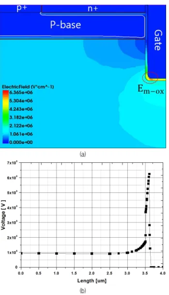
(a)
(b)
Fig. 2. OFF-state electric field (a) contour and (b) graph.
그림 2. OFF 상태에서 전계 (a) 윤곽선 및 (b) 그래프
그림 2는 4H-SiC trench gate MOSFET에서 각 부분의 전계를 보여주는 그림과 그래프이다. 4H-SiC trench gate MOSFET은 Junction BV가 발생하기 전에 Oxide에서 먼저 깨지므로 Oxide BV가 일어 나기 때문에, 전계 세기가 Oxide에서 가장 큰 것을 볼 수 있다. 특히, Edge 부분에 전계가 가장 집중 되고 그 수치가 6.2MV/cm이다.
2. Epi depth split
Epi depth의 변화에 따라서, Depletion region의
크기와 전계 분산 정도가 변하기 때문에 Epi depth 가 각각 15um, 20um, 25um에 따른 전계와 BV의 변화를 확인하였다.
(a) (b) (c)
(d)
Fig. 3. Field contour (a) 15um (b) 20um (c) 25um and (d) a graph in the OFF state in accordance with epi depth.
그림 3. Epi depth에 따른 OFF 상태에서 전계 윤곽선 (a) 15um (b) 20um (c) 25um 및 (d) 그래프
그림 3은 OFF 상태일 때, Epi depth에 따른 각 부분의 전계를 보여주는 그림과 그래프이다. Epi depth가 증가할수록 Depletion region이 Epi의 끝 부분까지 확장되고 그만큼 전계가 더 많이 분산되 므로 최대 전계는 6.7MV/cm, 6.2MV/cm, 5.3MV/
cm로 낮아진다.
Table 2. BV according to the epi depth of 4H-SiC trench gate MOSFET.
표 2. 4H-SiC trench gate MOSFET의 Epi depth에 따른 BV
Epi depth Breakdown voltage
15 um 1122.9 V
20 um 1347.9 V
25 um 1626.7 V
표 2는 Epi depth에 따른 BV의 시뮬레이션 결과 이다. 시뮬레이션 결과를 살펴보면, Epi depth가 증 가할수록 전계가 더 분산되어서 오래 버틸 수 있기 때문에 Epi depth가 15um, 20um, 25um일 때, BV 는 1122.9V, 1347.9V, 1626.7V로 Epi depth가 증가 할수록 BV는 높아진다.
Table 3. Ron according to the epi depth of 4H-SiC trench gate MOSFET.
표 3. 4H-SiC trench gate MOSFET의 Epi depth에 따른 Ron
Epi Depth Ron
15 um 16.8 mΩ
20 um 21.6 mΩ
25 um 26.6 mΩ
표 3는 Epi depth에 따른 Ron이다. Epi depth가 증가할수록 동일한 Drain 전압에 대해서 낮은 Drain 전류가 흐르기 때문에 Ron이 증가하고 이를 통해 서 BV와 Ron이 Trade-off 관계임을 알 수 있다.
3. Trench depth split
Trench depth의 변화에 따라서 Trench gate oxide 와의 Drift 거리와 전계 분산 정도가 다르기 때문에 Trench depth가 각각 1.5um, 2.0um, 2.5um에 따른 전계와 BV의 변화를 확인하였다.
그림 4는 Trench depth에 따른 각 부분의 전계를 보여주는 그림과 그래프이다. Trench depth가 감 소할수록 Trench gate oxide와의 Drift 거리가 멀 어지고 전계가 Epi 끝부분까지 분산되기 때문에 최 대 전계가 감소하고 Breakdown이 더 늦게 일어난 다. 따라서, 최대 전계는 6.5MV/cm, 6.2MV/cm, 5.9MV/cm로 낮아지는 경향성을 보인다.
(a) (b) (c)
(d)
Fig. 4. Field contour (a) 15um (b) 20um (c) 25um and (d) a graph in the OFF state in accordance with trench depth.
그림 4. Trench depth에 따른 OFF 상태에서 전계 윤곽선 (a) 1.5um (b) 2.0um (c) 2.5um 및 (d) 그래프
Table 4. BV according to the trench depth of 4H-SiC trench gate MOSFET.
표 4. 4H-SiC trench gate MOSFET의 Trench depth에 따른 BV
Trench Depth Breakdown voltage
1.5 um 2006.4 V
2.0 um 1347.9 V
2.5 um 1243.7 V
표 4는 Trench depth에 따른 BV의 시뮬레이션 결과이다. Trench depth가 1.5um, 2.0um, 2.5um일 때, BV는 2006.4V, 1347.9V, 1243.7V로 Trench depth 가 감소할수록 BV는 높아진다.
Table 5. Ron according to the trench depth of 4H-SiC trench gate MOSFET.
표 5. 4H-SiC trench gate MOSFET의 Trench depth에 따른 Ron
Trench Depth Ron
1.5 um 24.9 mΩ
2.0 um 21.6 mΩ
2.5 um 20.2 mΩ
표 5는 Trench depth에 따른 Ron이다. Trench depth가 감소할수록 동일한 Drain 전압에 대해서 낮은 Drain 전류가 흐르기 때문에 Ron이 증가하고 이를 통해서 BV와 Ron이 Trade-off 관계임을 알 수 있다.
4. Trench depth to epi depth
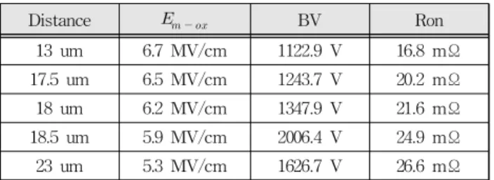
Table 6. Maximum electric field and BV according to distance from trench depth to epi depth.
표 6. Trench 깊이에서 Epi 깊이까지의 거리에 따른 최대 전계와 BV
Distance BV Ron
13 um 6.7 MV/cm 1122.9 V 16.8 mΩ 17.5 um 6.5 MV/cm 1243.7 V 20.2 mΩ 18 um 6.2 MV/cm 1347.9 V 21.6 mΩ 18.5 um 5.9 MV/cm 2006.4 V 24.9 mΩ 23 um 5.3 MV/cm 1626.7 V 26.6 mΩ
지금까지, Epi depth에 따른 최대 전계와 BV와 Trench depth에 따른 최대 전계와 BV와 Ron의 경 향성을 확인하였다. 본 절에서는 Epi depth Split과 Trench depth split을 토대로 Trench depth에서 Epi depth까지 거리의 변화에 따른 최대 전계와 BV와 Ron의 경향성을 보고자 하였다. 표 6은 Epi depth split과 Trench depth split을 토대로 Trench depth에서 Epi depth까지의 거리에 따른 최대 전계 와 BV 그리고 Ron을 나타내었다. 최대 전계에 대 해서는 모든 변수에서 거리가 길수록 Trench gate oxide까지의 Drift 거리가 멀어지고 전계가 더 넓게 분산되기 때문에 최대 전계가 감소하는 경향을 보 인다. BV는 거리가 18.5um일 때, 2006.4V로 가장
높고 나머지에 대해서는 거리가 멀수록 높은 BV를 가지는 경향성을 보인다. 마지막으로 Ron에 대해 서는 거리가 멀수록 높은 Ron값이 나타났고 BV와 Trade-off 관계임을 알 수 있다.
Ⅲ. 결론
본 논문에서는 4H-SiC trench gate MOSFET 설 계 시 적용되는 전기적 특성 변수에 대한 비교 및 분석을 수행하였다. 4H-SiC trench gate MOSFET 은 BV가 감소하는 단점이 있기 때문에 Epi depth split, Trench depth split, Trench depth to epi depth split으로 최대 전계와 BV와 Ron의 경향성을 확인 했다. Epi depth를 15um, 20um, 25um로 Split한 결 과, Epi depth가 증가할수록 최대 전계는 감소하고 BV와 Ron은 증가하는 경향성을 보인다. 그리고 Trench depth를 1.5um, 2.0um, 2.5um로 Split한 결 과, Trench depth가 감소할수록 최대 전계는 감소 하고 BV와 Ron은 증가하는 경향성을 보인다. 마지 막으로 Epi depth split과 Trench depth split을 토 대로 Trench depth에서 Epi depth까지의 거리를 13um, 17.5um, 18um, 18.5um, 23um로 Split한 결과, 거리가 증가할수록 최대 전계는 감소하고 18.5um 일 때 가장 높은 BV 값을 가지지만 이를 제외하면 거리가 증가할수록 BV가 증가하며, 거리가 증가할 수록 Ron은 증가하는 경향성을 보인다. 그러므로 BV를 높이기 위해서는 Epi depth를 증가시키고 Trench depth를 감소시켜야 하지만 BV와 On저항 은 Trade-off 관계이기 때문에 BV가 증가할수록 On저항도 증가한다. 따라서, 소자의 사용 목적에 따라 BV를 맞추는 것이 중요한데, 본 논문에서는 1200V급 4H-SiC trench gate MOSFET 설계가 목 적이기 때문에 10%의 마진까지 고려하였을 때, BV가 1320V 이상이 나와야한다. 그러므로, Epi depth가 20um, 25um일 때의 1347.9V, 1626.7V와 Trench depth가 2.0um, 2.5um일 때의 1347.9V, 2006.4V에서 1200V급 이상이라고 할 수 있다.
References
[1] Baliga BJ, Silicon carbide power device, Springer, 2009.
[2] Chen L, Guy OJ, Jennings MR, Igic P, Wilks
SP, Mawby PA, “Study of 4H-SiC trench MOSFET structures,” Solid-State Electr, Vol.49, No.7, pp.
1081-1085, 2005. DOI: 10.1016/j.sse.2005.05.003 [3] Šimonka V, Nawratil G, Hössinger A, Weinbub J, Selberherr S, “Anisotropic interpolation method of silicon carbide oxidation growth rates for three- dimensional simulation,” Orig Solid-State Electr, Vol.128, pp.135-140, 2017.
DOI: 10.1016/j.sse.2016.10.032a
[4] Wang Y, Tian K, Hao Y, Yu CH, Liu YJ, Godignon P, “An optimized structure of 4HSiC U-shaped trench gate MOSFET,” IEEE Trans
Electr Dev, Vol.62, No.9, pp.2774-2778, 2015.
DOI: 10.1109/TED.2015.2449972
[5] Nakamura T, Nakano Y, Aketa M, Nakamura R, Mitani S, Sakairi H, et al. Proc IEEE international
electron devices meeting, Vol.26, No.5, pp.1-3,
2011.[6] H. Takaya, J. Morimoto, T. yamamoto, J.
Sakakibara, Y. Watanabe, N. Soejima, K. Hamada,
“Materials Science Forum” Vols.740-742, pp.683-686, 2013.
BIOGRAPHY
Je-Wook Woo (Member)
2019:BS degree in Electrical Engineering, SeoKyeong University.
2019~:Unified course of the master’s in Electronics and Engineering, DanKook University.
Jeong-Ju Seo (Member)
2018:BS degree in Electrical Engineering, DanKook University.
2018~:Unified course of the master’s in Electronics and Engineering, DanKook University.
Seung-Hoo Jin (Member)
20120:BS degree in Electrical Engineering, DanKook University.
2020~:Unified course of the master’s in Electronics and Engineering, DanKook University.
Yong Seo-Koo (Member)
1981:BS degree in Electronics Engineering, Sogang University.
1983:MS degree in Electronics Engineering, Sogang University.
1992:Ph.D degree in Electronics Engineering, Sogang University.
Current research interest:integrated circuit, micro processor.