A B
그림
표
< 2-1> Comparison of thickness measurement result (UV nano imprinted polymer) Nanospec Nano indentation Error Reference 336 nm -Point 1 115 nm 103 nm -11 % Point 2 136 nm 133 nm -2 % Point 3 227 nm 205 nm -10 % Point 4 242 nm 225 nm -7 % Point 5 292 nm 287 nm -2 % Point 6 307 nm 310 nm 1 % Point 7 311 nm 310 nm 0 % Point 8 310 nm - -Point 9 312 nm 312 nm 0 % Point 10 253 nm 255 nm -1 % N o rm ali ze d D isp la ce m e nt [h /t] 0 1 2 3 4 5 Mo du lu s [ G P a ] 0 20 40 60 80 1 00 1 20 P o int 1 P o int 2 P o int 3 P o int 4 P o int 5 P o int 6 P o int 7 P o int 9 P o int 1 0 그림
그림
< 2-4> Schematic of nano pillar compression test using a nanoindentation apparatus
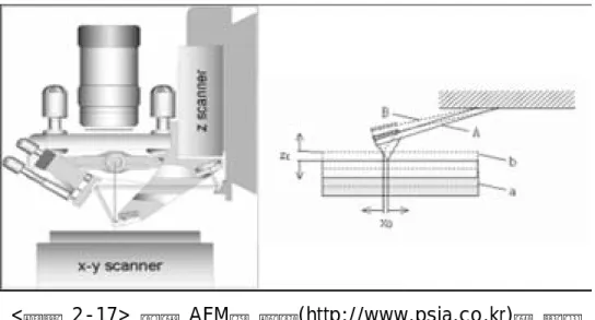
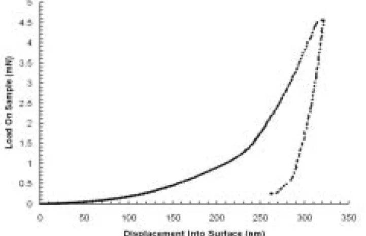
μ
μ μ
μ μ
그림
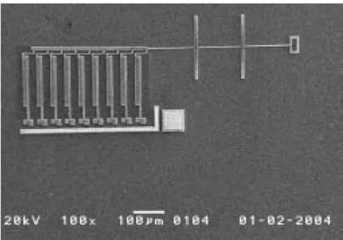
그림 공정으로 제작된 열구동기와 시편 < 2-7> MEMS
Cycles to Failure, Nf [Cycles]
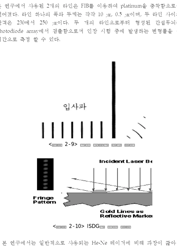
그림 이중 슬릿의 간섭 현상 < 2-9>
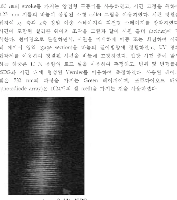
그림 의 측정 원리
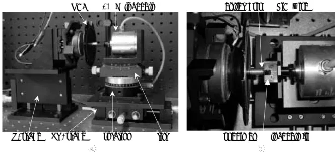
Z-stage XY-stage rotation tilt 10 N loadcell
VCA collet grip & SiC wire
specimen & loadcell jig
그림 를 이용한 피로 시험기
< 2-12> VCA
(a) (b)
그림
를 이용한 결과 를 이용한 결과
(a) ISDG (b) Vernier
그림 폴리 실리콘의 인장시험 결과 < 2-14> Cyc le [#] 1 00 101 1 02 103 1 04 105 1 06 107 1 08 109 1010 1 011 1012 Peak St re ss [ G Pa] 1 S harpe et al. Kahn et al. Kapel s et al. Muh lstein et al. S harpe long-term la st wo r k t his wo r k t his wo r k C ycle [ #] 100 101 102 103 1 04 1 05 1 06 1 07 1 08 1 09 1010 1011 1012 Peak St res s [G Pa] 0 . 7 0 . 8 0 . 9 1 . 0 1 . 1 1 . 2 1 . 3 1 . 4 1 . 5 1 . 6 1 . 7 S harpe et al. Kahn et al. Kapels et al. Mu hls tein et al. S harpe lon g-term
la st w or k S tat isti cal g ra ph Plo t 7 R e gr
그림 폴리 실리콘의
그림 으로 측정된
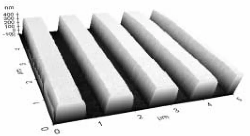
그림 상용 의 구조 와 물성 < 2-17> AFM (http://www.psia.co.kr)
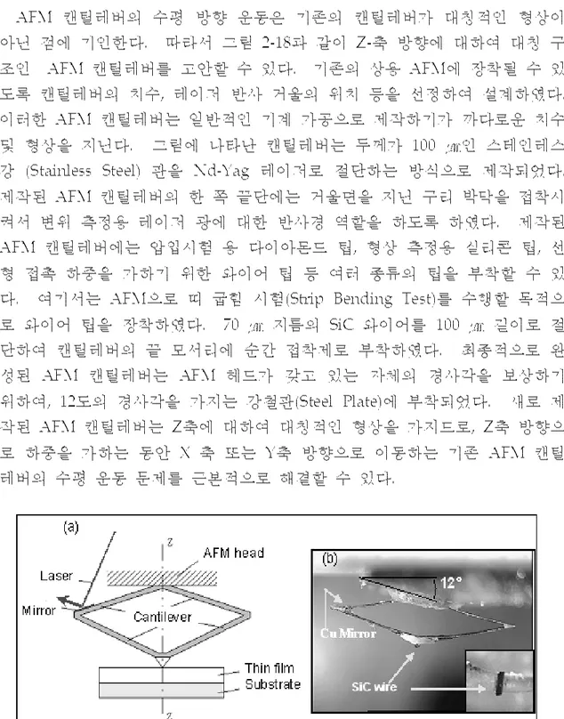
그림 축에 대칭적인 캔틸레버 제작된 캔틸레버
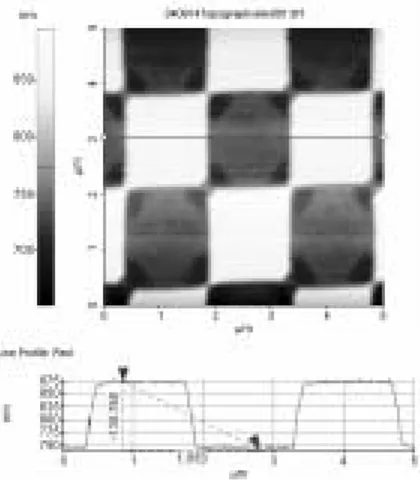
그림 전압과 스캐너 변위 곡선
Z-그림 띠굽힘시험 방법의 개략도 < 2-21>
그림 힘보정 이용 자유지지 금박막
< 2-22> AFM
그림
< 2-23> Rhombus shaped SCS cantilever fabricated by micro-manufacturing technique and enlarged view of a flat tip. SEM images of the flat tip (a) before and (b) after FIB polishing process, and laser beam reflection part (c) before and (d) after the polishing process
Δ σ
Δ
그림
< 2-24> Experimental setup for the adhesion test using rhombus-shaped cantilever in AFM
그림
μ
μ
그림
< 2-26> Macroscopic and microscopic pictures of gecko foot
그림
그림
< 2-28> SEM images of polypropylene nano-hair arrays
μ
그림
< 2-29> Hardness and elastic modulus of cyclic olefin copolymer(a) and polypropylene(b)
μ μ
μ μ
μ μ
그림
< 2-30> Load vs. displacement curve between SCS flat tip and COC nano-hair arrays (upper) and COC bulk substrate (lower)
μ μ
그림
< 2-31> Load vs. displacement curve between SCS flat tip and polypropylene nano-hair arrays (upper) and polyprolypene bulk
그림
그림
< 2-33> Specimen fabrication process for strip bending test
(a) (b)
그림
< 2-34> Optical microscope images of (a) Molybdenum freestanding structure, and (b) Silicon nitride freestanding structure
0 3 0 00 0 6 0 00 0 9 0 00 0 1 20 00 0 1 50 00 0 -1 0 1 2 3 4 5 6 7 8 M o _s t rip _1 M o _s t rip _2 M o _s t rip _3 M o _s t rip _4 Load ( m N ) D isplac em ent (n m) 0 20 00 0 40 00 0 60 00 0 80 00 0 10 00 00 -0 .5 0 .0 0 .5 1 .0 1 .5 2 .0 2 .5 3 .0 3 .5 4 .0 S iN_ st rip _1 S iN_ st rip _2 S iN_ st rip _3 S iN_ st rip _4 S iN_ st rip _5 Load ( m N ) D is plac emen t (nm) (a) (b) 그림
< 2-35> Load-displacement curves for (a) Mo free-standing structure and (b) SiN free-standing structure measured by strip bending
![그림 폴리 실리콘의 인장시험 결과<2-14> Cyc le [#]1 001011 021031 041051 06 10 7 1 0 8 10 9 10 10 1 0 11 10 12PeakStress [GPa]1S harpe et al.Kahn et al.Kapel s et al.Muh lstein et al.S harpe long-termla st wo r kt his wo r kt his wo r k C ycle [ #]10010](https://thumb-ap.123doks.com/thumbv2/123dokinfo/5196150.116129/28.892.137.752.729.1098/그림-폴리-실리콘의-인장시험-peakstress-kapel-lstein-termla.webp)