Vol. 70, No. 3, March 2020, pp. 220∼225 http://dx.doi.org/10.3938/NPSM.70.220
Large Piezoelectric Coefficient of high Quality Mn-doped (K
0.5Na
0.5)NbO
3Thick film by Using a Laser Doppler Vibrometer
Hae Jin Seog · Bong Chan Park · Shinuk Cho · Tae Heon Kim
∗· Ill Won Kim
†Department of Physics and Energy Harvest-Storage Research Center, University of Ulsan, Ulsan 44610, Korea
Aman Ullah
Department of Physics and Energy Harvest-Storage Research Center, University of Ulsan, Ulsan 44610, Korea Department of Physics, University of Science and Technology, Bannu 28100, KPK, Pakistan
(Received 18 February 2020 : accepted 19 February 2020)
The development of lead-free ferroelectric and piezoelectric materials is required from the view- point of environmental preservation. Among various lead-free materials, (K0.5Na0.5)NbO3 (KNN) has attracted much attention due to its excellent ferroelectric and piezoelectric properties. In this study, high-quality Mn-doped (K0.5Na0.5)NbO3(KNMN) films were deposited on Pt/TiO2/SiO2/Si substrates by using the sol-gel method. For various numbers of coating cycles; the KNMN films have thicknesses of around 0.8, 1.0, 1.5 and 2.0 µm, respectively. The effective piezoelectric coeffi- cient (d33,eff) of the KNMN films was analyzed using a home-made laser Doppler vibrometer that could measure large millimeter-scale areas. The average d33,eff of a 2-µm-thick KNMN film was measured to be around 120 pm/V, which is comparable to those of lead-based materials and higher than those of other lead-free piezoelectric film alternatives.
PACS numbers: 77.55.fp, 77.55.hn, 77.84.−s
Keywords: Effective piezoelectric coefficient, Laser Doppler vibrometer, (K,Na)NbO3, Thick film, Lead-free
I. Introduction
The development of lead-free ferroelectric and piezo- electric films is a priority because it allows for compo- nents that generate no harmful waste when they are produced or discarded. Of the various lead-free candi- date materials, K0.5Na0.5NbO3 (KNN) thin films have attracted a great deal of attention due to their attrac- tive ferroelectric and piezoelectric properties [1,2]. How- ever, the major obstacle in the fabrication of KNN thin films is the high leakage current, which occurs as a result of the easy volatilization of Na and K, thereby greatly deteriorating the ferroelectric and piezoelectric perfor- mances [3]. Earlier studies have shown that an appro- priate amount of Mn-doping in a KNN thin film sig- nificantly reduced the leakage current and improved its
∗E-mail: [email protected]
†E-mail: [email protected]
overall performances [4,5]. For example, Deng et al. and Lee et al. fabricated an Mn-doped KNN film using the sol-gel method and reported that increasing valence state of Mn2+, which is substituted at the Nb5+site as Mn3+, plays an important role in reducing the number of both oxygen vacancies and holes [4,5]. Sol-gel techniques are appearing as a very promising methodology to achieve highly textured oxide thin films high purity, ultrahomo- geneity, low processing temperatures, and most signifi- cantly the possibility of making glasses of new composi- tions. So an intense effort is being carried out to develop routes for all chemically coated piezoelectric devices.
Various techniques have been used to measure the ef- fective piezoelectric coefficient of ferroelectric films [6–
18]. However, large discrepancies exist in the piezoelec- tric coefficient of thin films and these flaws cannot be easily differentiated on the basis of film quality, or by various measurement techniques [6]. One of the major
This is an Open Access article distributed under the terms of the Creative Commons Attribution Non-Commercial License (http://creativecommons.org/licenses/by-nc/3.0) which permits unrestricted non-commercial use, distribution, and reproduction in any medium, provided the original work is properly cited.
obstacles in measuring the piezoelectric coefficient is the bending of the substrate, which occurs during the actua- tion of piezoelectric film [6,7]. This is because the bend- ing of the substrate completely distorts the authenticity of the measurement. In fact, it is very difficult to pro- duce a homogeneous uniaxial stress on a film deposited on a thick substrate without generating a bending effect [6,7]. In order to reduce the substrate bending effect, various techniques have been modified and implemented thus far [11–18]. The piezoresponse force microscopy (PFM) analysis of the films with deposited top electrodes may also experience inaccuracies related to the substrate bending issue [7,9,10]. Single beam laser interferometry techniques have been used to eliminate the bending of the substrate, which results from the thickness dilation of the films [13]. The double beam interferometer was developed to remove the error introduced by substrate motion and bending [11]. It has been widely accepted as one of the most accurate methods for measuring the d33 coefficient of films. However, this method requires the sample surface to have a high reflectivity, and the mea- surement results are strongly influenced by the optical alignment [12]. Moreover, this technique is not particu- larly user-friendly as it needs steady conditions.
The laser Doppler vibrometer (LDV) system is the most versatile, simple, and accurate technique for mea- suring the effective piezoelectric coefficient of piezoelec- tric thin films [7,12–18]. It is relatively easy to obtain a characteristic d33,effcoefficient for large area (millimeter- scale) piezoelectric films. Most importantly, the LDV does not require the sample surface to have a high reflec- tivity. The vibration velocity of the sample is measured by the LDV system and the displacement of the sam- ple can be obtained by integration. Furthermore, to the best of our knowledge, the effective piezoelectric coeffi- cient measured by the LDV system has not been reported for Sol-gel synthesized KNN-based films.
In this study, (K0.5Na0.5)(Mn0.005Nb0.995)O3
(KNMN) films with various thicknesses were fab- ricated using the sol-gel deposition method on Pt/TiO2/SiO2/Si(100) substrate. The crystal structure, microstructure, dielectric and ferroelectric properties of the KNMN films were analyzed. Our lab successfully set up an inexpensive home-made laser Doppler vibrometer system and investigated the effective piezoelectric
coefficient of the KNMN films by analyzing the spatial distribution of the displacement across the electrode using the LDV system.
II. Experimental details
For the preparation of (K0.5Na0.5)(Mn0.995Nb0.995)O3
(KNMN) films, sodium acetate, potassium acetate, nio- bium pentaethoxide, and manganese acetate were mixed in a solvent of 2-methoxyethanol and acetic acid. To compensate for the loss of alkaline metals during ther- mal annealing, 10 mol% excess K and Na were added to precursor solutions. The concentration of the final KNMN solution was adjusted to 0.4 mol/L. The KNMN films were grown on a Pt/TiO2/SiO2/Si(100) substrate using spin coating with a rate of 3000 rpm for 30 s. The wet film was dried at 400 ◦C for 7 min on a hot plate and then the dried gel film was calcined at 660 ◦C for 3 min in an air atmosphere using a box furnace. These steps were 10 times to synthesize KNMN thick film with thickness of around 0.8 µm. The 10 layers KNMN thick film was deposited additional 10 layers after annealed at 400 ◦C for 5 min on the hot plate and then we got the 20 layers KNMN thick film with thickness of around 1.0 µm. These steps were repeated 30 and 40 times to syn- thesize KNMN thick films with thicknesses of around 1.5 and 2.0 µm, respectively. The KNMN films were finally annealed at 660◦C for 30 min in an air atmosphere.
The crystal structures of the films were analyzed us- ing an X-ray diffractometer (XRD, X’pert PRO MRD, Phillips) with an 18-kW source and a Cu Kα line (λ ∼ 1.54 Å). The microstructure of the film was analyzed using field emission scanning electron microscopy (FE- SEM, JSM-6500F, JEOL). For electrical measurements, Pt top electrodes with areas of 2.5 × 10⁻⁴ cm2 were deposited on the KNMN films through a metal shadow mask using DC sputtering. The P − E hysteresis loop was measured using a ferroelectric tester (Precision LC, Radiant technologies, Inc.). The frequency-dependent dielectric constant and dielectric loss was measured by an impedance analyzer (HP4192A, Palo Alto) at room temperature. The effective piezoelectric coefficient of the film was measured using a home-made laser Doppler vi- brometer system.
Fig. 1. (Color online) Schematic of the experimental arrangement for piezoelectric characterization using a homemade laser Doppler vibrometer.
III. Results and discussion
Figure 1 shows the schematic diagram of the home- made laser Doppler vibrometer system for measuring the vibration velocity and displacement of the piezoelec- tric film. The apparatus consists of a function gener- ator (33210A, Agilent, USA), a laser Doppler vibrom- eter (AT500-05, Graphtec Corp., Japan), scan mirror (6215HB, Cambridge Tech., Cambridge, MA), an oscil- loscope (TDS3032B, Tektronix Inc., USA) and a high- voltage linear amplifier (F10A, FLC Electronics, Partille, Sweden). The change in displacement was measured us- ing the vibration velocity of the optical interferometer detector. The effective piezoelectric coefficient (d33,eff) can be expressed as: Vs,max = Aωs, where A denotes the displacement of the piezoelectric sample, Vs,max is the maximum value of the velocity and ωsis the angular frequency of the AC voltage, which is applied to vibrate the piezoelectric film [19,20].
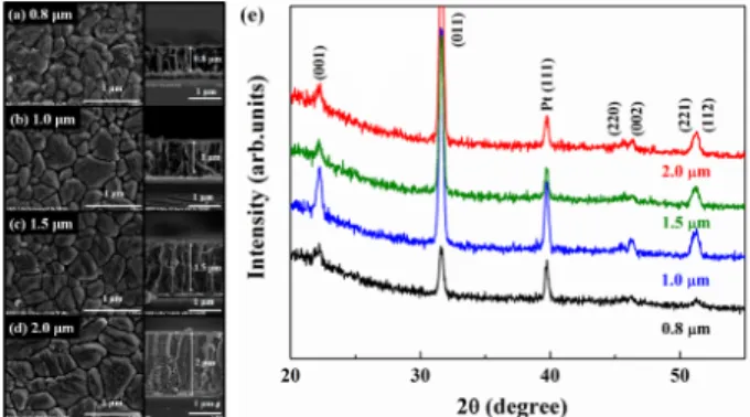
To check the quality of the fabricated thin films, FE- SEM was employed to image the morphology of the sur- faces and the cross-sections of the films. The FE-SEM micrographs of the surface and cross-sectional images of the KNMN films are provided in Fig. 2 (a-d). Note that the thicknesses of KNMN films were estimated from the cross-sectional images. With an increase in the number of coating cycles, the thicknesses of the KNMN films also increased, with thicknesses around∼ 0.8, 1.0, 1.5 and 2.0 µm. No obvious pores were noticed in the surface im- ages or in the cross-sectional images, demonstrating suc- cessful fabrication of the films. In addition, the surface
Fig. 2. (Color online) (a-d) Surface and cross-sectional morphologies of (K0.5Na0.5)(Mn0.005Nb0.995)O3
(KNMN) films with different thicknesses and (e) the XRD patterns of (K0.5Na0.5)(Mn0.005Nb0.995)O3
(KNMN) films with different thicknesses.
micrographs reveal that all of the KNMN films are very uniform and the grains are homogeneously distributed.
An increase in the average grain size of the films was ob- served with an increase in the film thickness. The X-ray diffraction (XRD) patterns of KNMN films with various thicknesses in the 2θ range of 20 – 60◦ are depicted in Fig. 2(e). The XRD measurements of the films were per- formed using a glancing angle configuration to eliminate the contribution of the substrate. The XRD patterns re- vealed good crystallinity of the films. A pure perovskite phase without any unwanted secondary phases was ob- tained in all of the KNMN films [21].
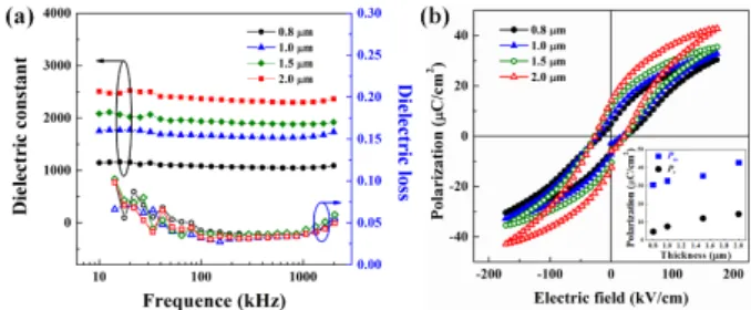
Figure 3(a) displays the dielectric constant and dielec- tric loss of KNMN films with thicknesses of 0.8, 1.0, 1.5 and 2.0 µm as function of various frequencies. The di- electric constant and loss curves of all films showed a slight decline with increasing frequency. The dielectric constant of a KNMN film strongly depends on the film thickness. An obvious increase in the dielectric constant can be noticed with an increase in the film thickness from 0.8 to 2.0 µm. However, the dielectric loss is roughly in- dependent of the film thickness. Generally, a thickness- dependent dielectric constant can be explained by the interface dead layer model [21–23]. The thickness of the dead layer is thought to be independent of the total film thickness. One or more interfacial dead layers are con- sidered to exist between the KNMN film and top elec- trode in the form of an interfacial capacitor. Moreover, the dielectric constant also depends on the grain size of the films [22]. In this study, the improvement in the dielectric constant of KNMN films can be attributed to
Fig. 3. (Color online) (a) The dielectric constant and dielectric loss of KNMN films with different thickness of 0.8, 1.0, 1.5 and 2.0 µm and (b) the ferroelectric P-E hys- teresis loops of KNMN films with different thicknesses.
The inset shows the maximum and remnant polarization of KNMN films with different film thicknesses.
the increase in average grain size with thickness modifi- cation, which can reduce the number and size of grain boundary defects, as shown in Fig. 2(a-d).
Figure 3(b) presents the polarization hysteresis loops of KNMN films with different thicknesses (0.8, 1.0, 1.5 and 2.0 µm). Generally, cation and anion vacancies are considered major obstacles in measuring the polarization hysteresis loop of pure KNN thin films because of the volatility of K and Na [1]. These defects originate from the compositional fluctuation of K and Na in KNN film and the degree of oxidation under heat treatment, as has been reported for KNN single crystals [3]. These defects (oxygen and alkaline ions vacancies) in KNN films act as space charge, which cause deterioration in the elec- trical properties of the crystalline film and single crystal [1,3]. The substitution of Mn in the KNN film was re- ported to decrease the hole concentration by increasing the valence of Mn2+ion, thereby improving the electrical performances of KNMN [4,5]. In this study, all KNMN exhibited a saturated polarization hysteresis loop with definite values of remnant and maximum polarization, which is in agreement with previously reported studies [5].
The variations of the remnant and maximum polariza- tion in the KNMN films as a function of film thickness are plotted in the inset of Fig. 3(b). Both the remnant and maximum polarization are strongly thickness-dependent, however the coercive field is roughly independent. The remnant polarization increased from 4.8 µC/cm2to 14.2 µC/cm2 as the film thickness increased from 0.8 µm to 2.0 µm. In a similar fashion, the maximum polarization increased from 30 µC/cm2 to 42 µC/cm2. The increase
of remnant and maximum polarization showed an en- hancement of approximately 33% and 40%, respectively.
The enhancement in polarization parameters with an in- crease in film thickness can be explained on the basis of the dead layers [23]. The thinner KNMN film with a Pt electrode consists of more than one thin dead layer, which usually results in a lower dielectric constant due to the resistive dead layers. The dead layer consumes a partial bias after the voltage is applied. Consequently, the smaller Pr of the thinner KNMN film is attributed to a weaker driving electric field. In contrast, the thicker film receives a stronger electric field and is less affected by the dead layers, which delivers a larger Prvalue [23].
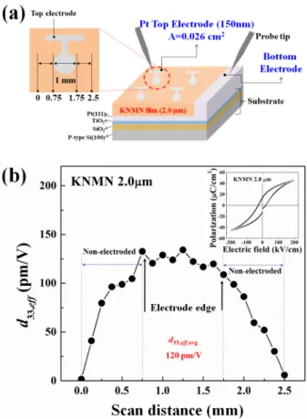
Figure 4(a) shows a schematic representation of the grown thin film (thickness : 2.0 µm) on a Pt/TiO2/SiO2/Si(100) substrate with a top Pt electrode (diameter : 1mm). The film area is denoted by the color orange, while the color grey represents the top electrode of the film. By analyzing the piezoelectric response of a relatively large area covered by an electrode, we measure the piezoelectric displacement of the active part (the elec- troded area) and the surrounding passive part (the non- electroded area) of the film, and then precisely estimate the out-of-plane piezoelectric displacement. The effec- tive piezoelectric coefficient (d33,eff) was measured using an LDV system. In our measurement system, the laser beam tip of the interferometer was relatively large (diam- eter : 20 µm); this size reduces measurement inaccuracies that can result from the small tip of the PFM system, particularly for the large area of piezoelectric response of the top electrode of the sample. Figure 4(b) plots the calculated effective piezoelectric coefficient (d33,eff) of the KNMN film (thickness : 2.0 µm) as a function of scan distance while the corresponding polarization hys- teresis loop is shown in the inset of Fig. 4(b). The piezoelectric capacitor was excited by applying a sinu- soidal AC-voltage and a frequency of 8 kHz. We mea- sured the spatial distribution of the displacement across the electrode-covered area (diameter : 1 mm) and the massive parts of either side along the scan line (the scan distance included : 0.75 mm on each side of the bound- ary of the electrode). It can be seen from Fig. 6(b) that d33,eff gradually decreases with an increasing scan dis- tance from either side of the active part. However, in
Fig. 4. (Color online) (a) Metal/Ferroelectric/Metal (MFM) capacitor structure for measuring device using the laser Doppler vibrometer (LDV) system. (b) Effec- tive piezoelectric coefficient (d33,eff) of the KNMN 2.0 µm-thick film. The inset shows the P-E hysteresis loop of the KNMN film.
the active part, the d33,eff shows nearly constant behav- ior.
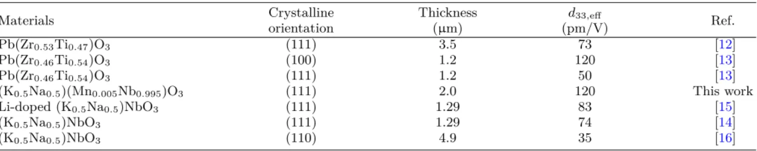
The average value of d33,eff,avg of the KNMN film cal- culated from the active part was : 120 pm/V. This is comparable to those of lead-based counterparts [12,13]
and higher than alternatives among lead-free ferroelec- tric films [14–16], as summarized in Table 1. As demon- strated in Table 1, in comparison with other KNN-based thin film, the 120 pm/V value was much greater than that of 35-83 pm/V attained for other KNN-based and lead-free thick films [15–18]. As PZT-based films have high d33 values ranging from 50 – 120 pm/V [6] by mea- suring LDV system. The KNMN film suggests that this material can be considered a viable alternative for lead- free piezoelectric devices.
Generally, in KNN thin films alkaline ion vacancies are formed due to the volatilization of alkali ions during the pyrolysis process, accompanied by oxygen vacancies [1,3,
5,24]. During high temperature annealing, the oxidation of oxygen vacancies Vo′′ in the KNN films as expressed by equation (1) [26,27].
Vo′′+1
2O2→ O2−+ 2h· (1) Where Vo′′ and O2− denote the oxygen vacancy and the oxide-ion site, respectively, and h·indicates the free car- rier holes. It can see that Vo′′and h·coexist in the KNN films. In other words, the formation of holes can de- crease the amount of oxygen vacancies but results in the increase in leakage current [3,5]. However, the introduc- tion of Mn2+Nb can absorb these holes by increasing the valance of Mn2+Nb can absorb these holes by increasing the valance of Mn2+Nb as expressed by equation (2) and (3) [5,25].
Mn2+Nb+ h·→ Mn3+Nb (2)
Mn3+Nb+ h·→ Mn4+Nb (3) The substitution of Mn is demonstrated suppressing leakage current, improving ferroelectricity and the va- lence increase of Mn is indicated to play an important role in electron-hole absorption during oxidation. More- over, the large grain size of the Mn-doped KNN film contributes to the high d33,eff value. For the films with large grain size, a large piezoelectric response is expected because it is easy for the domain to rotate. These results indicate that the KNN film with a small concentration of Mn-dopant is an attractive candidate lead-free piezoelec- tric material system for replacing the PZT-based piezo- electric films.
IV. Conclusion
In this study, high quality KNMN films with thick- nesses between 0.5 and 2.0 µm were fabricated using the chemical solution deposition. All of the KNMN films exhibited a perovskite structure. FE-SEM analysis re- vealed pore free morphologies both on the surface and in cross-sectional images. The dielectric constant increased with increasing thickness from 0.8 to 2.0 µm due to a corresponding increase in the average grain size. An in- crease in the remnant and maximum polarization was
Table 1. Effective piezoelectric coefficients properties of KNMN film compared with lead-based and lead-free thick films measured using a laser Doppler vibrometer system.
Materials Crystalline
orientation
Thickness (µm)
d33,eff
(pm/V) Ref.
Pb(Zr0.53Ti0.47)O3 (111) 3.5 73 [12]
Pb(Zr0.46Ti0.54)O3 (100) 1.2 120 [13]
Pb(Zr0.46Ti0.54)O3 (111) 1.2 50 [13]
(K0.5Na0.5)(Mn0.005Nb0.995)O3 (111) 2.0 120 This work
Li-doped (K0.5Na0.5)NbO3 (111) 1.29 83 [15]
(K0.5Na0.5)NbO3 (111) 1.29 74 [14]
(K0.5Na0.5)NbO3 (110) 4.9 35 [16]
also found with an increase in film thickness. The KNMN film with a 2 µm thickness exhibited a high piezoelectric coefficient d33,eff,avg of : 120 pm/V, which is compara- ble to those of lead-based films and higher than lead-free counterparts measured with the LDV system. Our re- sults suggest that KNMN films could potentially be use- ful for applications in lead-free piezoelectric devices, such as micro-actuator devices.
ACKNOWLEDGEMENTS
This work was supported by the National Re- search Foundation of Korea (NRF) grant funded by the Korea government (Ministry of Education) [2017R1D1A1B03036032 and 2017R1D1A1B03028614].
REFERENCES
[1] C.W. Ahn et al., J. Phys. D: Appl. Phys. 42 , 215304 (2009).
[2] L. Wang, K. Yao and W. Ren, Appl. Phys. Lett.
93, 092903 (2008).
[3] Y. Kizaki, Y. Noguchi and M. Miyayama, Appl.
Phys. Lett. 89, 142910 (2006).
[4] Q. Deng et al., J. Mater. Chem. C 3, 8225 (2015).
[5] S.Y. Lee et al., Curr. Appl. Phys. 11, S266 (2011).
[6] A. Barzeger, D. Damjanovic, N. Ledermann and P.
Muralt, J. Appl. Phys. 93, 4756 (2003).
[7] G.J.T. Leighton and Z. Huang, Smart Mater.
Struct. 19, 065011 (2010).
[8] C. Andrews, Y. Lin, H. Tang and H.A. Sodano, J.
Intell. Mater. Syst. Struct. 22, 1879 (2011).
[9] Y. Lin and H.A. Sodano, Adv. Funct. Mater. 19, 592 (2009).
[10] A. Jalalian et al., Appl. Phys. Lett. 104, 103112 (2014).
[11] S. Sivaramakrishnan et al., Appl. Phys. Lett. 103, 132904 (2013).
[12] Z. Wang and J. Miao, J. Phys. D:Appl. Phys. 41, (2008) 035306.
[13] R. Herdier et al., Rev. Sci. Instrum. 77, 093905 (2006).
[14] P.C. Goh, K. Yao and Z. Chen, Appl. Phys. Lett.
97, 102901 (2010).
[15] P.C. Goh, K. Yao and Z. Chen, Appl. Phys. Lett.
99, 092902 (2011).
[16] L. Wang et al., Ceram. Int. 38, S291 (2012).
[17] S.A. Chae et al., Curr. Appl. Phys. 16, 429 (2016).
[18] S. Shetty, J. Yang, J. Stitt and S. Trolier-McKinstry, J. Appl. Phys. 118, 174104 (2015).
[19] W. Osten, Optical Inspection of Microsystems (CRC Press, USA, 2006), pp.245-292.
[20] O.D.L. Rochefoucauld, S.M. Khanna and E.S. Ol- son, J. Acoust. Soc. Am. 117, 1267 (2005).
[21] S.Y. Lee et al., Jpn. J. Appl. Phys. 51, 09MD03 (2012).
[22] X.J. Lou and J. Wang, J. Phys.: Condens. Matter 22 055901 (2010).
[23] F. Yang et al., Appl. Phys. Lett. 106, 172903 (2015).
[24] L. Wang et al., Appl. Phys. Lett. 97, 072902 (2010).
[25] Y. Inagaki and K. Kakinoto, Appl. Phys. Express 1, 061602 (2008).
[26] R. Ding et al., J. Am. Ceram. Soc. 96, 3530 (2013).
[27] S. E. Cummins and L. E. Cross, J. Appl. Phys. 39, 2268 (1968).