• 검색 결과가 없습니다.

Surface and Electrical Properties of 2 wt% Cr-doped Ni Ultrathin Film Electrode for MLCCs

N/A
N/A
Protected

Academic year: 2021

Share "Surface and Electrical Properties of 2 wt% Cr-doped Ni Ultrathin Film Electrode for MLCCs"

Copied!
4
0
0

로드 중.... (전체 텍스트 보기)

전체 글

(1)

224 J. Sensor Sci. & Tech. Vol. 24, No. 4, 2015 Journal of Sensor Science and Technology

Vol. 24, No. 4 (2015) pp. 224-227 http://dx.doi.org/10.5369/JSST.2015.24.4.224 pISSN 1225-5475/eISSN 2093-7563

Surface and Electrical Properties of 2 wt% Cr-doped Ni Ultrathin Film Electrode for MLCCs

Haena Yim, JinJu Lee, and Ji-Won Choi

+

Abstract

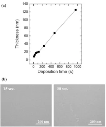
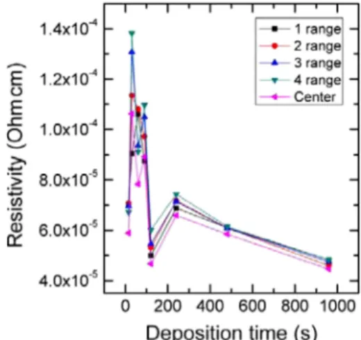
In this study, 2 wt% Cr-doped Ni thin films were deposited using DC sputtering on a bare Si substrate using a 4 inch target at room temperature. In order to obtain ultrathin films from Cr-doped Ni thin films with high electrical properties and uniform surface, the micro- structure and electrical properties were investigated as a function of deposition time. For all deposition times, the Cr-doped Ni thin films had low average resistivity and small surface roughness. However, the resistivity of the Cr-doped Ni thin films at various ranges showed large differences for deposition times below 90 s. From the results, 120 s is considered as the appropriate deposition time for Cr-doped Ni thin films to obtain the lowest resistivity, a low surface roughness, and a small difference of resistivity. The Cr-doped Ni thin films are prospective materials for microdevices as ultrathin film electrodes.

Keywords: Cr-doped Ni, Metal electrode, Electrical properties, Ultrathin films electrode, MLCCs, Sputtering

1. INTRODUCTION

Electronic devices have become smaller and lighter in the past years, and therefore, the components in the devices also need to be made smaller and lighter. Among the various components, a metal thin film is considered as an essential material for bottom, inner, and top electrodes in a device. For example, it is necessary to fabricate ultrathin dielectric films with ultrathin inner electrode films below ~20 nm for manufacturing small-sized multilayer ceramic capacitors (MLCCs) [1], which are the most frequently used elements in current electronic devices such as displays, computers, and cellular phones. Many conventional methods have been reported to obtain electrode films, for example, the wet deposition method with copper or nickel nanoparticles, tape casting, and the screen-printing process. However, these methods include nanoparticle slurries and have a limit on the thickness range below ~0.8 µm [2], owing to the mechanical instability of thin films. Thus, physical deposition methods such as molecular beam epitaxy (MBE), pulsed laser deposition, or sputtering are

considered as emerging approaches. In the case of metal films deposited through the physical deposition method, the metal films have the electrically isolated behavior at the beginning of growing the thin film due to its discontinuous area. Because the isolated parts of the thin film start to combine, the electrical resistance decreases rapidly when the thickness of the metal thin film is increased. Once it starts coalescing, the metal electrodes are formed as a thin film and show resistivity as low as that of metal electrodes.

The Ni electrode is a representative material [3] for various applications. It is not only used in MLCCs [4], but also in thin film transistors [5] and resistors [6] because of its considerable resistance to oxidation and a low temperature coefficient of resistance. However, Ni has ferromagnetic properties around room temperature [7], which result in a low sputtering yield [8].

Therefore, we improved the sputtering yield of the Ni target by reducing ferromagnetism through Cr doping. The purpose of this paper is to research the surface and electrical properties of 2 wt%

Cr-doped Ni ultrathin film electrodes for microdevice [9].

Therefore, we will be confirming the critical thickness of Cr- doped Ni ultrathin films with good surface roughness and low resistivity.

2. EXPERIMENTAL

In this study, 2 wt% Cr doped Ni thin films were deposited using DC sputtering on a bare Si substrate (20 mm × 20 mm) at Center for Electronic Materials, Korea Institute of Science and Technology,

Seoul 136-791, Korea

+

Corresponding author: [email protected] (Received: July 14, 2015, Accepted: July 21,2015)

This is an Open Access article distributed under the terms of the Creative Commons Attribution Non-Commercial License(http://creativecommons.org/

licenses/bync/3.0) which permits unrestricted non-commercial use, distribution,

and reproduction in any medium, provided the original work is properly cited.

(2)

Surface and Electrical Properties of 2 wt% Cr-doped Ni Ultrathin Film Electrode for MLCCs

225 J. Sensor Sci. & Tech. Vol. 24, No. 4, 2015 room temperature. The working pressure was 3 mTorr under pure

Ar atmosphere during the sputtering. Further, Cr-doped Ni thin films were deposited at various deposition times (10–960 s). A DC power of 30 W was applied to the Cr-doped Ni target (4 inch).

The cross-section and surface of Cr-doped Ni thin films were measured by Nova SEM (Nova-200, FEI Company), and the electrical properties were investigated through Hall measurement.

The surface roughness was measured using atomic force microscopes (AFM, Veeco). The structural properties of Cr-doped Ni were investigated using X-ray diffraction (XRD, Rigaku).

2. RESULTS AND DISCUSSIONS

Fig. 1 (a) shows the thickness profile of 2 wt% Cr-doped Ni thin films as a function of deposition time; their thickness was increased linearly with deposition time. Because Cr-doped Ni thin films deposited at 10 s have a very low thickness, the thickness was difficult to confirm using Nova SEM. Fig. 1 (b) shows the surface image of Cr-doped Ni thin films at deposition times 15, 30 s. Although there are very short deposition times, they formed thin films not isolated. Therefore, Cr-doped Ni thin films have an advantage for ultrathin film electrodes because they form thin films in a short time.

The electrical properties of 2 wt% Cr-doped Ni thin films as a function of deposition time are shown in Fig. 2; they had a low resistivity in all ranges of deposition time. The lowest resistivity of Cr-doped Ni thin films is 5.674 × 10

-5

Ohm.cm at a deposition time of 120 s considering thickness. Therefore, Cr-doped Ni thin film electrodes are potential materials with low resistivity despite their very low thickness.

Fig. 3 shows the XRD patterns of Cr-doped Ni thin films as a function of deposition time. All thin films indicated that Cr-doped Ni thin films were easily crystallized at room temperature without a secondary phase [10]. Further, Cr-doped Ni thin films had a high Ni intensity in XRD patterns for the longest deposition time. The XRD shows low Ni intensities for deposition times 30, 60, and 90 s because the thickness of the Cr-doped Ni thin films was thin.

Obviously, all Cr-doped Ni thin films on the bare Si substrate show a Si substrate peak.

Fig. 4 (a) shows the surface roughness of Cr-doped Ni thin films as a function of deposition time, and it shows that all thin

Fig. 1. (a) Thickness profile of Cr-doped Ni thin films as a function of deposition time (b) Surface image at deposition time of 15 and 30 s.

Fig. 2. Electrical properties of Cr-doped Ni thin films as a function of deposition time.

Fig. 3. XRD patterns of Cr-doped Ni thin films as a function of dep- osition time.

I 11 I

(3)

Haena Yim, JinJu Lee, and Ji-Won Choi

J. Sensor Sci. & Tech. Vol. 24, No. 4, 2015 226 films had a small RMS value under 0.4 nm. The RMS value of electrodes is an important factor because component materials for ultrathin MLCC dielectric layer thickness. Recently, a 1 µm dielectric layer has been commercialized. Thus, Cr-doped Ni thin film electrodes are a promising material for ultrathin film electrodes. Further, the smallest RMS value of Cr-doped Ni thin

films was 0.167 nm for a deposition time of 120 s. In common with SEM surface image, we needed to confirm whether the Cr- doped Ni formed thin film is isolated. Fig. 4 (b) shows the AFM images of Cr-doped Ni thin films for deposition times 10, 15 s, which are form of thin film. Despite the short deposition times, Cr-doped Ni thin films substrained as thin films.

Fig. 5 shows the regional electrical resistivity difference according to the deposition time for Cr-doped Ni thin films. A regional resistivity difference of the films was investigated through Hall measurement to confirm its macro thickness uniformity. Since resistivity depends on thickness, it can be changed in terms of the uniformity of the Cr-doped Ni thin films.

The size of the sample was 20 mm × 20 mm. The 1st, 2nd, 3rd, and 4th ranges indicate that the Cr-doped Ni thin film sample was divide into four equal parts (5 mm × 5 mm), and the center indicates the inside center of Cr-doped Ni thin film (5 mm × 5 mm).

As shown in Fig. 5, the difference of regional resistivity reduced with an increasing thickness of the Cr-doped Ni thin films. The higher the deposition time, the more uniform is the thin films.

However, the thin films had a large difference of regional resistivity for deposition times below 90 s. It means that the thickness of the thin films is inconsistent.

Based on these results, the Cr-doped Ni thin film had the lowest resistivity and small RMS value for the deposition time of 120 s.

Further, the difference of regional resistivity has a small value, relatively. Therefore, the deposition time of the Cr-doped Ni thin films was selected to be 120 s to fabricate ultrathin film electrodes for microdevices.

3. CONCLUSIONS

In this study, 2 wt% Cr-doped Ni thin films were successfully deposited on a bare Si substrate by DC sputtering at room temperature. They have a uniform surface and form thin films at all deposition times. In the XRD patterns, Cr-doped Ni thin films indicated crystallization of Ni at room temperature without requiring a secondary phase. Cr-doped Ni thin films had electrical properties as good as metal electrodes. At the deposition time of 120 s, the resistivity and RMS value of Cr-doped Ni thin films were 5.674 × 10

-5

Ohm.cm and 0.167 nm, respectively. Further, the difference of resistivity shows a small value for a deposition time of 120 s. Therefore, 2 wt % Cr-doped Ni thin films are promising materials as ultrathin film electrodes for microdevices such as MLCCs.

Fig. 4. (a) Surface roughness of Cr-doped Ni thin films as a function of deposition time (b) AFM images of Cr-doped Ni thin films at deposition time 10 and 15 s.

Fig. 5. Electrical properties at various ranges in Cr-doped Ni thin film sample (20 mm ×20 mm).

I 12 I

(4)

Surface and Electrical Properties of 2 wt% Cr-doped Ni Ultrathin Film Electrode for MLCCs

227 J. Sensor Sci. & Tech. Vol. 24, No. 4, 2015

ACKNOWLEDGMENT

This research was supported by the Core Technology of Materials Research and Development Program (no. 10041232) funded by the Ministry of Knowledge Economy, Republic of Korea.

REFERENCES

[1] H. Yim, S.-Y. Yoo, S. Nahm, S.-J. Hwang, S.-J. Yoon, and J.-W. Choi, “Synthesis and dielectric properties of HCa2Nb3O10 layered structure ceramics”, Ceramics Inter- national, Vol. 39, No. 1, pp. 611-614, 2013.

[2] T. Tsurumi, “Technology in the future of high capacity mul- tilayer ceramics capacitor”, Mater Integr., Vol. 21, pp. 59- 70, 2008.

[3] G. Nocerino, and K. Singer, “The electrical and compo- sitional structure of thin Ni-Cr films”, Thin Solid Films, Vol.

57, No. 2, pp. 343-348, 1979.

[4] Y. Nakano, T. Nomura, and T. Takenaka, “Residual stress of multilayer ceramic capacitors with Ni-electrodes (Ni- MLCCs)”, Japanese journal of applied physics, Vol. 42, No. 9B, pp. 6041, 2003.

[5] Y. Seol, J. Lee, and N.-E. Lee, “Effects of different elec- troplated gate electrodes on electrical performances of flex-

ible organic thin film transistor and flexibility improvement”, Organic Electronics, Vol. 8, No. 5, pp. 513- 521, 2007.

[6] C. Lee, B. Kang, M. Lee, S. Ahn, G. Stefanovich, W.

Xianyu, K. Kim, J. Hur, H. Yin, and Y. Park, “Elec- tromigration effect of Ni electrodes on the resistive switch- ing characteristics of NiO thin films”, Physics Letters, Vol.

91, No. 8, pp. 082104-082104-3, 2007.

[7] W. Gong, H. Li, Z. Zhao, and J. Chen, “Ultrafine particles of Fe, Co, and Ni ferromagnetic metals”, J Appl Phys, Vol.

69, No. 8, pp. 5119-5121, 2007.

[8] K. Kawabata, T. Tanaka, A. Kitabatake, K. Yamada, Y.

Mikami, H. Kajioka, and K. Toiyama, “High rate sputtering for Ni films by an rf-dc coupled magnetron sputtering sys- tem with multipolar magnetic plasma confinement.” Jour- nal of Vacuum Science & Technology A: Vacuum, Surfaces, and Films, Vol. 19, No. 4, pp. 1438-1441, 2001.

[9] Y. Kwon, N.-H. Kim, G.-P. Choi, W.-S. Lee, Y.-J. Seo, and J. Park, “Structural and surface properties of Ni-Cr thin films prepared by DC magnetron sputtering under variation of annealing conditions.” Microelectronic engineering, Vol.

82, No. 3, pp. 314-320, 2005.

[10] C.-M. Wang, D. R. Baer, S. M. Bruemmer, M. H. Engel- hard, M. E. Bowden, J. A. Sundararajan, and Y. Qiang,

“Microstructure of the native oxide layer on Ni and Cr- doped Ni nanoparticles.” Journal of nanoscience and nan- otechnology, Vol. 11, No. 10, pp. 8488-8497, 2011.

I 13 I

수치

Fig. 3 shows the XRD patterns of Cr-doped Ni thin films as a function of deposition time
Fig. 4. (a) Surface roughness of Cr-doped Ni thin films as a function of deposition time (b) AFM images of Cr-doped Ni thin films at deposition time 10 and 15 s

참조

관련 문서

Abstract The electrochemical reaction between lead borate glass frit doped with Sn metal filler and Ni-Cr wire of a J-type resistor during a term of Joule heating is

Abstract The electrical and optical properties of fluorine-doped tin oxide films grown on polyethylene terephthalate film with a hardness of 3 using electron cyclotron

We investigated the characteristics of oxygen plasma treatment on the surface, structural, and physical properties of TiO 2 films prepared at various

Effect of Al 2 O 3 oxide buffer layers on the optical and electrical properties of sputtered ZnO films were intensively investigated for developing the

In this study, crystalline and electrical properties of CuO doped (Ba,Sr)TiO 3 ceramics were investigated to determine the low temperature sintering

Electrical properties of the Al doped ZnO thin films fabricated by RF magnetron sputtering system with working pressure and oxygen contents.. Jong-Wook Kim † and

Controlling the surface energy and electrical properties of carbon films deposited using unbalanced facing target

Various compositions of Al doped ZnO thin films deposited at substrate temperatures between 0 and 250 °C were explored to find excellent electrical and optical