1. INTRODUCTION
Transparent conducting oxide(TCO) films are materials, which are electrically conductive and highly transparent to visible light. TCOs have been extensively investigated because of their important technological applications in regards to many fields such as organic light emitting diodes(OLEDs), flat panel displays(FPDs), surface acoustic waves(SAW) and solar cells[1-4]. Zinc oxide (ZnO) thin films have been considered as transparent conducting films because they are more stable against hydrogen plasma, more abundant, and less expensive than indium tin oxide(ITO) which has superior electrical and optical properties in this field.
ZnO has intrinsic defects, such as Zn interstitials(Zn
i) and O vacancies(V
o). They allow non-stoichiometric ZnO to have intrinsic n-type conductivity with high electron densities. However, electrical properties of ZnO films are not good in comparison with ITO when native point defects don’t affect to ZnO as donors efficiently. So, many researchers have been focused on the intentional doping in ZnO, such as Al doped ZnO(AZO) and Ga doped ZnO (GZO). Especially, Al doped ZnO films have some advantages such as high temperature stability and higher transmittance even at near infrared wavelengths compared
to ITO[5]. Many researchers have reported about AZO thin films according to the different doping content of Al[6-8].
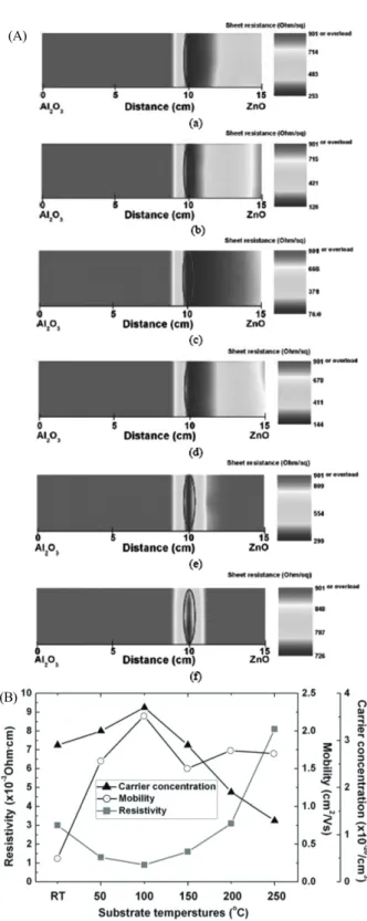
However, there is a still controversy concerning the optimized Al doping concentration in ZnO. In this study, a full range of AZO compositions and various growth temperatures of AZO thin films were investigated by continuous composition spread(CCS). CCS is a thin film growth method for various compositions on a substrate with a binary or ternary composition spread [9-13]. Full compositions of Al
xZn
1-xO are deposited on a glass substrate at different temperature by CCS. Especially, we focused on the effect of various substrate temperatures on the physical properties of varying Al doped ZnO films by continuous composition spread. Also, their properties such as structural, electrical and optical properties were examined.
2. DESIGN
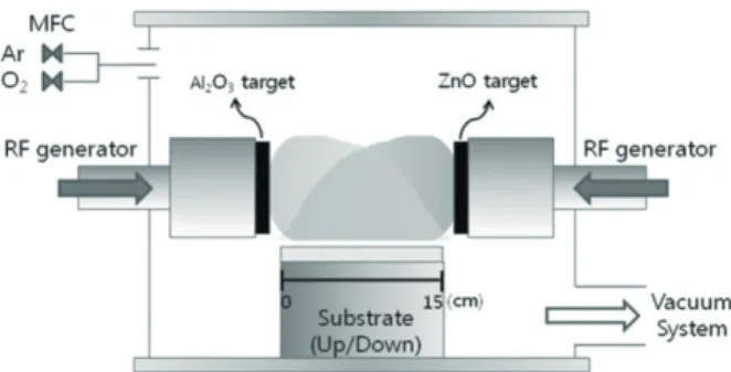
Al doped ZnO thin films were deposited on a square sample(15 cm × 2 cm)(eagle 2000, corning) at various substrate temperatures by off-axis sputter-CCS shown as Fig.
1. The off-axis sputter CCS has three independent radio frequency(RF) magnetron sputtering guns, which are located at 90° to the substrate. A zinc oxide(purity 99.99
%, CERAC) and Al
2O
3(purity 99.99 %, CERAC) targets were used to explore the superior electrical and optical properties of AZO. The sputtering chamber was pumped down to 2.66 × 10
-4Pa by a rotary pump and turbo
1
Electronic Materials Research Center, Korea Institute of Science and Technology
2
Interface Control Research Center, Korea Institute of Science and Technology
+