P2-58 / K. Bae
IMID 2009 DIGEST •
Abstract
Electrical and optical properties of SiO2-doped ZnO (SZO) films on the corning 7059 glass substrates by using rf-magnetron sputtering method are investigated. The deposition rate becomes maximum near 3 wt.% and gradually decreases when the SiO2 content further increases. The growth rates at 3 wt.% is 4 °A/s. We found that the average transmittance of all films is over 80% in the wavelength range above 500 nm. The optical band gap decreases from 3.52 to 3.33 eV with an increase in thickness. X-ray diffraction patterns show that the film with a relatively low SiO2 content (< 4 wt.%) is amorphous. SZO films at the SiO2 contents of 2 wt.% shows the resistivity of about 3.8 ×10⁻³·cm. The sheet resistance decreases with increasing the heat treatment temperature.
1. Introduction
Transparent and conductive oxide (TCO) films are very important because they have been widely used as transparent electrodes for optoelectronic devices such as touch panels, flat panel displays, and thin-film solar cells. Research to develop TCO thin films with a low resistivity as well as a high transmittance in the visible range has been conducted using various binary and ternary metal oxide compounds. So far, In2O3-SnO2 (ITO) films have mainly been used as materials for TCO films. However, it was found that they have often been limited in their application because of the frequent necessity to optimize electrical, optical, and chemical properties for specialized applications [1]. For example, ITO films have a substantial problem that they should be grown at a relatively high temperature (> 300℃) to get a low resistivity and a high transmittance in the visible range [2]. The amorphous ITO film deposited at a low temperature has a low resistance to moist heat, which leads to a degradation of the conductivity and the light transmittance with time . For the purpose of improving TCO film properties, new materials consisting of multi component oxides have attracted much attention [4, 5]. On the other hand, the low temperature growth of TCO films is
very important because plastic substrates such as polyethylene terephthalate (PET) and poly carbonate (PC) was recently proposed as a new substrate for TCO film growth due to their several advantages such as light weight, low cost, thinness, and resistance to breakage [5–7]. As one method to overcome the problem found in ITO films, several groups have studied electrical and optical properties of In2O3-ZnO (IZO) films [1, 4, 5, 8, 9]. This is because, in the case of IZO films grown at room temperature on the corning glass, their resistivity is comparable to that of conventional ITO films(∼10−4·cm) and have the average transmittance of over 90 % in the visible range. However, world consumption of indium is increasing and the price will be expensive in near future. Thus, a development of impurity-doped ZnO thin films without using In2O3 will be necessary as a new material for TCO films. In this paper, we fabricated SiO2-doped ZnO (SZO) films on the corning 7059 glass substrates by using rf-magnetron sputtering method and investigated electronic and optical properties such as transmittance, the growth rate, and the sheet resistance.
2. Experimental
SiO2 and ZnO powders were mixed with various composition ratios and was calcined at 1000℃ in air for 2 hours to make a 2 inch diameter target. Then, the deposition of SiO2- doped ZnO films is carried out at room temperature in a pure Ar gas pressure of 2×10⁻³ torr with a rf-power of 60 W. The electrical and optical properties of SiO2-doped ZnO films were investigated as functions of composition ratio and film thickness. Their crystallography and surface morphologies were also observed by using a XRD pattern and a SEM or AFM image. Electrical sheet resistance was measured by the 4-point probe method and electrical resistivity and carrier concentration were measured using the van der Paw method. The optical transmission through the film was measured in the wavelength range from 200 to 800 nm. The film thickness was measured by using α-step (VEECO Co.) and Spectra Thick 2000 Ellipsometer.
Electrical and optical Properties SiO
2doped ZnO film
transparent conductive oxide(TCO)
Kang Bae
*1,Sung-Won Ryu
1, Jae-Suk Hong
2, Jeong-Sik Park
1,
Seoung-Hwan Park
1, Hwa-Min Kim
1Dept. of Electronics & Display, Catholic University of Daegu, 330 Hayang-Eup, Gyeonsan-Si, Gyeongbuk, Republic of Korea1
330 CTC Co., 330 Hayang-Eup, Gyeonsan-Si, Gyeongbuk, Republic of Korea2
P2-58 / K. Bae
• IMID 2009 DIGEST
Fig. 1. Shows the deposition rate as a function of
the SiO2 content (wt.%) for SiO2-doped ZnO(SZO)
films.
Figure 1 shows the deposition rate as a function of the SiO2 content (wt.%) for SiO2-doped ZnO (SZO) films deposited by rf-magnetron sputtering process. The SiO2 contents are varied from 2 to 5 wt.%. The deposition rate becomes maximum near 3 wt.% and gradually decreases when the SiO2 content further increases. The growth rates at 3 wt.% is 4 Å/s. Generally, the sheet resistance (Rs) of a film is inversely proportional to the film thickness (d) as Rs = p/d, where means the resistivity of the film. As the deposition time becomes long, the sheet resistance is reduced because d is determined by the product of the average deposition rate and the deposition time. Thus, the information on the deposition rate at a given SiO2 content is important to control the sheet resistance.
Fig. 2. shows transmission spectra and (αhν)2 vs hν of SiO2-doped ZnO (SZO) films for several.
Figure 2 shows transmission spectra and (αhν)2 vs hν of SiO2-doped ZnO (SZO) films for several film thicknesses. The average transmittance of all films is over 80% in the wavelength range above 500 nm. On the other hand, the average transmittance rapidly decreases when the wavelength is below 500 nm. We know that the
transmittance of SZO films is comparable to that of IZO films [10]. In the fundamental absorption region, the transmittance T is given by following equation;
T = Aexp-αt, (1)
where A, α, and t are a constant, the absorption coefficient, and the thickness of the film, respectively. Then, since (A≒1) near the absorption edge, we can obtain α for a given t from Eq. (2). The resulting α can be used to find the optical band gap from the following equation for a direct allowed semiconductor:
αhν = A′ (hν − Eog)1/2, (2)
where, Eog and A′ are the optical band gap and a constant, respectively. If the plots of (αhν)2 vs hν give rise to a straight line, the film can be regarded as a direct allowed semiconductor and the optical band gap is given by extrapolating the straight line to the h_ axis. It should be noted that the band edge absorption is shifted toward the lower energy with increased thickness. The estimated optical band gap decreases from 3.52 to 3.33 eV with an increase in thickness, as shown in the inset of Fig. 2, and is probably due to the quantum effect [11, 12].
Fig. 3. shows resistivity and Hall mobility as a function of the SiO2 content (wt.%) for SiO2-doped ZnO (SZO)
films prepared by rf -magnetron sputtering..
Figure 3 shows resistivity and Hall mobility as a function of the SiO2 content (wt.%) for SiO2-doped ZnO (SZO) films prepared by rf magnetron sputtering. In the investigated rane of the SiO2 content, the resistivity largely increases with increasing the SiO2 content while Hall mobility rapidly decreases. SZO films at the SiO2 contents of 2 wt.% shows the resistivity of about 3.8 ×10⁻³ ·cm, which is larger than that of ITO films(∼4×10⁻⁴ ·cm). Thus, we know that further optimization will be necessary to obtain films with resistivity comparable to ITO films. The Hall mobility (µ) shows values between 2 and 20 cm2/V s in a investigated range of the SiO2 content. The increase of the Hall mobility may be attributed to the increase in the electron
P2-58 / K. Bae
IMID 2009 DIGEST • concentration.
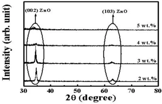
Fig. 4. x-ray diffraction patterns of SiO2-doped ZnO
(SZO) films.
Figure 4 we plotted x-ray diffraction patterns of SiO2-doped ZnO (SZO) films prepared by rf -magnetron sputtering process. The micro-structure of SZO films deposited by rf -magnetron sputtering method is shown to depend on the SiO2 content contained in deposited films. That is, the film with a relatively low SiO2 content (< 4 wt.%) is microcrystalline. On the other hand, films changes to be amorphous as the SiO2 content increases.
4. Summary
In summary, we investigated electrical and optical properties of SiO2-doped ZnO (SZO) films on the corning 7059 glass substrates by using rf-magnetron sputtering method. We found that the average transmittance of all films is over 80% in the wavelength range above 500 nm. X-ray diffraction patterns show that the film with a relatively low SiO2 content (<4 wt.%) is amorphous. SZO films at the SiO2 contents of 2 wt.% shows the resistivity of about 3.8 ×10⁻³·cm. It is found that the sheet resistance decreases with increasing the heat treatment temperature.
Acknowledgement
Some of the graduate students are participating in the second stage of BK21
5. References
[1] T. Minami, T. Kakumu, and S. Takata, J. Vac. Sci. Technol. A 14, 1704 (1996).
[2] A. Kaijou, M. Ohyama, M. Shibata, K. Inoue, U. S. Patent, No. 5,972,527 (1999).
[3] R. K Jain, and R. C. Lind, J. Opt. Soc. Am. 73, 647 (1983).
[4] S. H. Park, H. M. Kim, B. R. Rhee, and E. Y. Gho, Jpn. J. Appl. Phys. 40, 1429 (2001).
[5] H. M. Kim, S. K. Jeung, J. S. Ahn, Y. J. Kang, and C. K. Je, Jpn. J. Appl. Phys. 42, 223 (2003).
[6] K. Noda, H. Sato, H. Itaya, and M. Yamada, Jpn. J. Appl. Phys. 42, 217 (2003).
[7]
S. Y. Sohn, H. M. Kim, S. H. Park, and J. J.
Lim, New Phys. 46, 332 (2003).
[8]
H. Hiramatsu, W. S. Seo, and K. Koumoto,
Chem. Mater. 10, 3033 (1998).
[9]
Y. Yan, S. J. Pennycook, J. Dai, R. P. H.
Chang, A Wang, and T. J. Marks, Appl. Phys
Lett. 73, 2585 (1998).
[10]
J. K. Lee, H. M. Kim, S. H. Park, J. J. Kim,
B. R. Rhee, and S. H. Sohn, J. Appl. Phys. 92,
5761 (2002).
[11]