다중 PIN-다이오드 포스트를 이용한, 향상된 감쇄량과 대역폭이 늘어난 도파관 리미터의 설계
무하마드 캄란 카탁1, 유선웅1, 강승택1, 유성룡2, 오동철2, 노돈석2, 윤성현3
Design of A Waveguide Limiter Having an Improved Attenuation and a Broadened Bandwidth by Using Multiple PIN-Diode Posts
Muhammad Kamran Kattak1, Seon-woong Yoo1, Sungtek Kahng1, Seongryong Yoo2, DongChul Oh2, DonSuk Roh2, and Songhyun Yun3
요 약
본 논문에서는, Ku 대역의 소형 도파관 리미터 설계를 기술한다. 기본적으로 16.125 GHz로부터 16.375 GHz의 주파수 범위에서 통과 특성을 가지며, 큰 전력의 유입 시, 차단특성이 나타난다. 덧붙이면, 협대역에서는 20 dB 이상, 상기 전체 대역에서는 50 dB 이상의 감쇄량을 가지는 대역차단 여파기로 전환가능한 구조가 요구된다. 따라서, 이를 만족하기 위해 Off상태에서는 대역통과 여파기로서 On상태에서는 대역차단 여파기 기능으로 스위칭 가능한 다중 PIN 다이오드 포스트를 갖춘 도파관 장치가 구현되어야 한다. 등가회 로모델링에서 출발하여 정확도 높은 전자장 분석기에서 구조 설계가 이뤄진다. 마지막으로, 설계결과가 요구성능에 부합하는지에 대해 논의된다.
Key Words : Limiter, Bandpass filter, Bandstop filter, PIN Diode, Waveguide, Radar
ABSTRACT
This paper deals with a size-reduced Ku-band waveguide limiter. Basically, it passes the signal from 16.125 GHz through 16.375 GHz, but when excessively high power is injected to the input port, it should change to a bandstop filter.
Furthermore, it is required to change to bring attenuation by more than 20 dB and 50 dB over a narrow band and the entire passband, respectively. Therefore, in order to meet this requirement, a limiting device is implemented with multiple PIN-diode posts that enable the limiter to be the bandpass filter and stopband one at the off and on states of the PIN-diode switch, respectively. So, the design goes through the equivalent circuit modelling and the geometry is realized in the accurate electromagnetic analysis CAD tool. Finally, the result is discussed to shed light on whether it complies with the aforementioned requirement.
※ The research has been supported by Critical Military Parts Localization Program(Project No. C140007) Funded by DTaQ.
1인천대학교 정보통신공학과 전파공학 및 전파환경 연구실, 2(주)엘트로닉스, 3국방기술품질원
**인천대학교 정보통신공학과 ([email protected]), 교신저자 : 강승택
I. INTRODUCTION
The limiter is used to protect a radar system from the incidence of high power microwave. Especially, since the receiving block of the radar equipment is built for a low level of power which is different from the transmitting one, the limiter is an indispensable part of it in the event of the incoming high power[1,2]. The sources of the high
power entering the receiving block may come from the air, but usually they are attributed to the leaked power of the transmitter in the same system.
For the purpose of treating the varying level of input power into the receiver of the radar, the limiter should have both the functions of passing and blocking a certain frequency band of microwave energy. When hazardous amount of electromagnetic wave comes in, the limiter
ought to be a bandstop filter of significant attenuation. If not, the limiter should behave as a bandpass filter. These two phases can be brought by the use of PIN-diode switches. As is well known, a PIN-diode provides the off and on states, and a inherent capacitance at the on-state[3,4]. The switches are adopted in the form of posts as in [1,2] or an iris in a waveguide segment as in[5,6]. Because the switching function and variable capacitance are required to impede the flow of the injected high power microwave for the attenuation mode and not to stop the propagation of the electromagnetic wave for the bandpass mode in the waveguide limiter, the PIN diode embedded posts penetrate the top-wall of the metallic waveguide into the internal space. The post is thin, which is proper to minimize the degradation of the transmission coefficient over the passband and overheating problems with low likelihood of the field concentration. On the contrary, the iris as a shaped slot formed in the metallic plane is easy to make and inserted between the waveguide sections. This is highly likely to degrade the insertion loss and cause a high voltage breakdown.
In this paper, a waveguide limiter is designed for the operation in a Ku-band ranging from 16.125 to 16.375 GHz. Three PIN-diode posts are placed instead of an iris to avoid high voltage malfunctions. The switching post is dissected to parts which are drawn in the CAD software.
At the off-states of the PIN diodes, the limiter is designed to pass the signal over the band. And, the attenuation takes place as greater than 20 dB for a narrow band with one PIN-diode on, and more than 50 dB over the entire band with all the switches on with capacitances. The equivalent circuit modelling is carried out and the frequency responses of the geometry are evaluated by the full-wave Electromagnetic analysis program. The results are compliant with the requirement of the switchable filters.
Ⅱ. BASIC SCHEME AND EQUIVALENT CIRCUIT
Prior to being geared up for the design process, the operational scheme of the waveguide limiter is briefly and pictorially mentioned.
(a) All the switches off : Energy passed
(b) One switch off : Energy attenuated to a degree
(c) All the switches on : Energy blocked
Figure 1. Basic scheme of the limiter
When all the PIN-diodes are off, the injected energy is transmitted with almost no loss as in Fig.1(a). As to an increased level of the input power, one switch is turned on and it should attenuate the incoming power at a narrow channel from the band as in Fig 1(b). The input power level is not allowable, and the PIN-diodes are all turned on to trap it over the entire band as in Fig. 1(c). This scheme can be explained by the following equivalent circuit.
(a) Configuration ; With PIN-diodes at the on-state, resistors are low and ignored here
(b) Frequency response of bandstop filtering Figure 2. Equivalent circuit and its feature
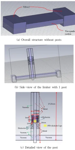
(a) Overall structure without posts
(b) Side-view of the limiter with 1 post
(c) Detailed view of the post
Figure 3. Building blocks of the waveguide limiter Fig. 2(a) shows the configuration of the equivalent
circuit of the bandstop filter, assuming all the PIN-diodes are at the on-state, which is represented by C's (Csh) in the 3 shunt resonators. The L's (Lsh) imply the inductance from the switching post, and series C's (Cse) consider the capacitance of the aperture for a post. The TX-line segment with and corresponds to the distance in the waveguide. Given WR-62 as the waveguide and PIN-diode as switches, , , , Cse and Lsh are set to 60o, 120o, 100, 0.23 pF and 0.48 nH, respectively.
Besides, Csh is given 0.18 pF, 0.19 pF and 0.2 pF from the first post to the third one in order. Then, we get Fig. 2(b) as the frequency response. As is obviously seen in the figure, the bandstop filter characteristics are obtained as S21 starts to fall from around 12 GHz and rise from 17 GHz.
We are aware that the current view-graph is too good to be true, but the equivalent circuit modelhas nothing but lumped elements and ideal transmission-line segments which do not follow the dispersion property of a metallic waveguide, and will end up with possible degradation in the frequency response for the waveguide environment.
Taking into account the change by the physical realization such as the bandwidth reduction as well as the frequency shift, it is tolerated to have a wider bandwidth and greater attenuation than the specifications in the stage of circuit simulation.
Ⅲ. Physical implementation of a waveguide limiter
Based on the equivalent circuit modelling, the limiter is realized in the form of a waveguide with the switching posts. We choose the WR-62 as the rectangular waveguide for port sections connected by a smaller one of 10.2×3.5×41.7mm3 in order to compensate for the frequency shift due to the loading of the posts.
Fig. 3(a) shows the bird's eye-view of the first building block of the waveguide limiter before the post is loaded.
When a PIN-diode post is placed as Fig. 3(b), the parts of the switch are elaborately drawn as Fig. 3(c) where the corresponding materials and physical dimensions for DC-bias are noted. Also, model DH60033-03 is taken into consideration. This one-post device can be tested, but its electrical effects are included in the following
configuration. The three PIN-diode posts are loaded sequentially in the middle section to work like Fig. 2(b).
As shown in Fig. 4(a), the three posts of the PIN-diode stand in line. The center-to-center distance between the neighboring posts is 10 mm. The first post is close to the input port to prohibit the maximum point of TE10-mode from occurring for protection, while the last post is 13.7 mm away from the output port. This structure gives the following electrical performances one by one in accordance with the off-off-off, on-off-off, off-on-off, off-off-on, and on-on-on states of the PIN-diodes 1, 2 and 3.
In the first place, all the PIN-diodes are turned off. This results in a bandpass filter as shown in Fig. 5(a). S21, equal to S12, becomes nearly 0 dB, which means the device passes the incoming microwave power. Simultaneously, the return loss is quite acceptable as |S11| equaling around -15 dB. This bandpass filtering effect disappears as at least one out of the three switches is on. Fig.'s 5(b), (c),
(a) 3D view of the multiple-post limiter
(b) Side-view of the multiple-post limiter Figure 4. Physical shape of the multi-post limiter
(b) Narrow-band attenuation ; on-off-off state
(c) Narrow-band attenuation ; off-on-off state
(d) Narrow-band attenuation ; off-off-on state
(e) Wide stopband and bigger attenuation ; on-on-on state Figure 5. Frequency responses of the waveguide
limiter vs. combinations of PIN-diode states greater than 20 dB over narrow channels from the
specified band. This could be predicted by thinking that only one shunt resonator is working and makes one pole.
Last but definitely not least, to increase the level of attenuation from the one-pole cases, the three PIN-diodes should be turned on at the same time to make the poles as many as the three shunt resonators, which will drive the transmission coefficient to fall much rapidly. More importantly, 0.16 pF, 0.16 pF, and 0.18 pF are given to the capacitances of the PIN-diodes 1, 2 and 3, respectively, for the on-on-on state. As shown in Fig. 5(e), |S21| becomes lower than -50 dB, which will effectively limit the strength of the incoming power. Therefore, it can be said that the design results comply with the specifications mentioned earlier in the Ku-band.
(a) Bandpass effect ; off-off-off state of the PIN-diodes
IV. CONCLUSIONS
In this paper, a Ku-band limiter was designed for the protection of a radar system. The equivalent circuit model
that satisfies the bandpass and bandstop filters, when the shunt resonators are not working and available, respectively, was constructed to expect the frequency responses as required by the limiter. On the basis of the circuit modelling, the limiter was physically realized in the form of a relatively short waveguide having the PIN-diode posts. The design was verified to meet the requirements of the limiter by observing the electrical properties of good transmission, narrow-band attenuation and wide-band blocking according to the states of the PIN-diodes and capacitances. This device can be an effective way to limit the excessively large input power.
REFERENCES
[1] N. Roberts, "A review of solid-state radar receiver protection devices", Microwave Journal, vol. 34, no. 12, pp.121-122, Feb. 1991.
[2] R. F. Bilotta, "Receiver protections: a technology update", Microwave Journal, vol. 40, no. 8, Aug. 1997.
[3] http://www.macom.com/ShuntPIN.
[4] J. F. White, Microwave Semiconductor Engineering, Van Nostrand Reinhold Company INC, 1982.
[5] N. V. Drozdovski, and L. M. Drozdovskaia, "Microstrip and waveguide passive power limiters with simplified construction", J. Microwaves and Optoelectronics, vol. 1, no.
5, pp. 14-29, Dec. 1999J.
[6] J. S. Park,․B.-M. Kim, and Y. K. Cho, "Design and experiment of waveguide limiter with band-pass characteristics using PIN diode," The Journal Of Korean Institute Of Electromagnetic Engineering And Science, Vol. 23, No. 9, pp.1065∼1072, Sept. 2012.
저자
Muhammad Kamran Khattak 비회원
․2012년 2월:스웨덴 Linneaus 대학 (공 학석사)
․2014년 3월 ~ 현재:인천대학교 정보 통신공학과 박사과정
<관심분야> : 전자파 수치 해석 및 응용, EMI/EMC 대책, 초 고주파 부품, 안테나 광대역 흡수체, 설계, 메타재질구조 이 론 및 응용
유 선 웅(Seong-wonng Yoo) 비회원
․2010년 3월 ~ 현재:인천대학교 정보 통신공학과(공학사)
<관심분야> : 초고주파 부품 및 안테나
강 승 택(Sungtek Kahng) 정회원
․2000년 2월:한양대학교 전자통신 공 학박사
․2000년 4월:한양대학교 산업과학연구
소 연구원
․2004년 2월:한국전자통신연구원 통신 위성개발센터 선임연구원
․2004년 ~ 현재:인천대학교 정보통신 공학과 교수
․2007년 ~ 현재:송도 국방벤처 자문교수
․2007년 ~ 현재:한국통신학회 마이크로파 및 전파 연구회 간사 ∼ 위원장, 한국전자파학회 편집위원, 국제이사
․2014년 12월 대한전기학회 학술상 수상(광파 및 전자파 분 야)
<관심분야> : 전자파 수치 해석 및 응용, EMI/EMC 대책, 초 고주파 부품 및 안테나 설계, 메타재질구조 이론 및 응용
유 성 룡(Seongryong Yoo)
․2012년 7월:인천대학교 정보통신공학 과 석사
․2013년 6월 ∼ 현재:(주)엘트로닉스 연구소 선임 연구원
<관심분야> : 안테나 설계, 초고주파/밀리미터파 도파관 및 수동 부품 설계
오 동 철(Dongchul Oh) 비회원
․2004년 8월:홍익대학교 전파통신 공 학과 석사
․2005년 3월 ∼ 현재:(주)엘트로닉스 연구소 책임연구원
<관심분야> : 통신/위성 송수신 시스템
노 돈 석(Donsuk Roh) 비회원
․1986년 2월:경북대학교 전자공학과
․1986년 5월 ~ 2000년 10월: (주)삼성 항공/전자.탈레스 선임연구원
․2000년 10월 ~ 2002년 9월 : (주)텔웨 이브 무선사업 부장
․2002년 10월 ~ 현재 : (주)엘트로닉스 연구소장 및 사업 본부장
<관심분야> : 레이더 RF System, 통신/위성 송수신기, 차세 대 이동통신
윤 성 현(Yun, SongHyun)
․2001년 2월 : 부산대학교 컴퓨터공학 석사
․2009년 2월 : 경북대학교 전자컴퓨터 공학 박사(수료)
․2003년 ~ 현재 : 국방기술품질원 연구 원
<관심분야> : 초고주파 도파관, 반도체형 증력증폭기